

Page 1
Ordering number:2063A
PNP/NPN Epitaxial Planar Silicon Transistors
2SB1143/2SD1683
50V/4A Switching Applications
Applications
· Voltage regulators, relay drivers, lamp drivers,
electrical equipment.
Features
· Adoption of FBET, MBIT processes.
· Low saturation voltage.
· Large current capacity and wide ASO.
( ) : 2SB1143
Specifications
Absolute Maximum Ratings at Ta = 25˚C
retemaraPlobmySsnoitidnoCsgnitaRtinU
egatloVesaB-ot-rotcelloCV
egatloVrettimE-ot-rotcelloCV
egatloVesaB-ot-rettimEV
tnerruCrotcelloCI
)esluP(tnerruCrotcelloCI
noitapissiDrotcelloCP
erutarepmeTnoitcnuJjT 051
erutarepmeTegarotSgtsT 051+ot55–
C
PC
C
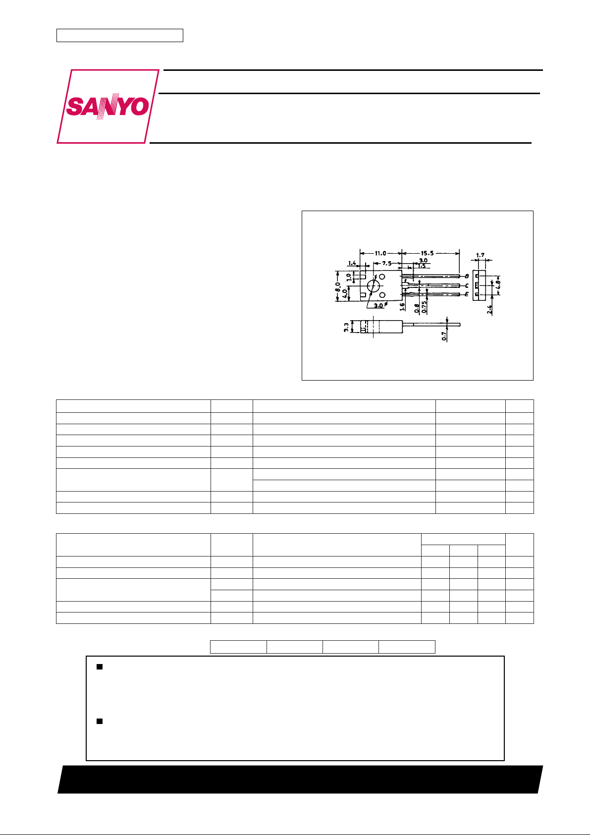
Package Dimensions
unit:mm
2042A
[2SB1143/2SD1683]
B : Base
C : Collector
E : Emitter
SANY O : TO-126ML
OBC
OEC
OBE
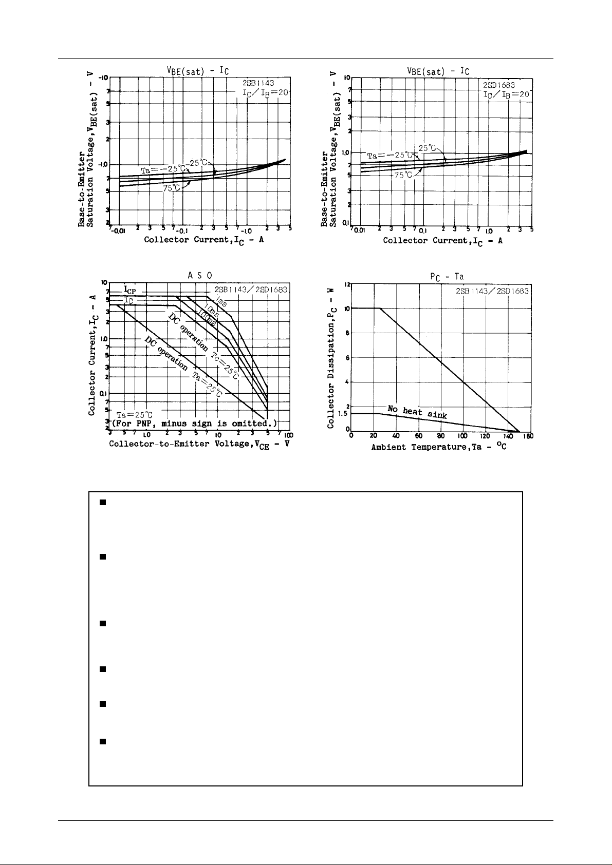
Tc=25˚C
06)–(V
05)–(V
6)–(V
4)–(A
6)–(A
5.1W
01W
˚C
˚C
Electrical Characteristics at Ta = 25˚C
retemaraPlobmySsnoitidnoC
tnerruCffotuCrotcelloCI
tnerruCffotuCrettimEI
niaGtnerruCCDh
hEF2VECI,V2)–(=
tcudorPhtdiwdnaB-niaGf
ecnaticapaCtuptuOC
* ; The 2SB1143/2SD1683 are classified by 100mA hFE as follows :
V
OBC
OBE
EF
T
bo
BC
V
BE
1VECI,V2)–(=
V
EC
V
BC
002R001082S041004T002065U082
Any and all SANYO products described or contained herein do not have specifications that can handle
applications that require extremely high levels of reliability, such as life-support systems, aircraft’s
control systems, or other applications whose failure can be reasonably expected to result in serious
physical and/or material damage. Consult with your SANYO representative nearest you before using
any SANYO products described or contained herein in such applications.
SANYO assumes no responsibility for equipment failures that result from using products at values that
exceed, even momentarily, rated values (such as maximum ratings, operating condition ranges,or other
parameters) listed in products specifications of any and all SANYO products described or contained
herein.
I,V04)–(=
0=1)–(Aµ
E
I,V4)–(=
0=1)–(Aµ
C
C
C
I,V01)–(=
C
Am001)–(=
A3)–(=
Am05)–(=
zHM1=f,V01)–(=52)93(Fp
nimpytxam
SANYO Electric Co.,Ltd. Semiconductor Bussiness Headquaters
TOKYO OFFICE Tokyo Bldg., 1-10, 1 Chome, Ueno, Taito-ku, TOKYO, 110-8534 JAPAN
92098HA (KT)/4137KI/D176TA, TS No.2063–1/4
sgnitaR
*001*065
04
051zHM
tinU
Page 2
2SB1143/2SD1683
retemaraPlobmySsnoitidnoC
egatloVnoitarutaSrettimE-ot-rotcelloCV
egatloVnoitarutaSrettimE-ot-esaBV
egatloVnwodkaerBesaB-ot-rotcelloCV
egatloVnwodkaerBrettimE-ot-rotcelloCV
egatloVnwodkaerBesaB-ot-rettimEV
emiTNO-nruTt
emiTegarotSt
emiTllaFt
I
)tas(EC
I
)tas(EB
I
OBC)RB(
I
OEC)RB(
I
OBE)RB(
no
gts
f
I,A2)–(=
C
C
C
C
E
B
I,A2)–(=
B
R,Am1)–(=
Am001)–(=
Am001)–(=49.0)–(2.1)–(V
I,Aµ01)–(=
0=06)–(V
E
=∞ 05)–(V
EB
I,Aµ01)–(=
0=6)–(V
C
tiucriCtseTdeificepseeS07)07(sn
tiucriCtseTdeificepseeS
tiucriCtseTdeificepseeS53)03(sn
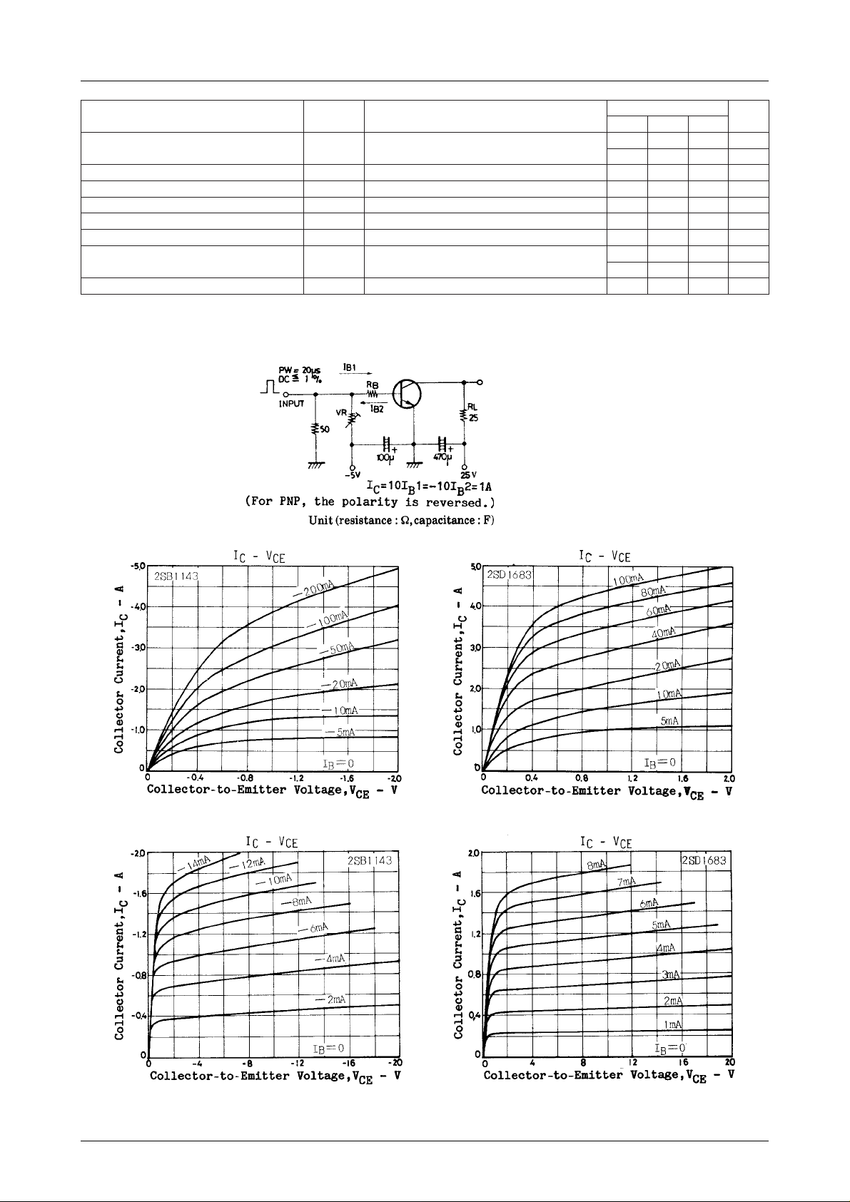
Switching Time Test Circuit
sgnitaR
nimpytxam
)053–()007–(Vm
091005Vm
)054(sn
056sn
tinU
No.2063–2/4
Page 3

2SB1143/2SD1683
No.2063–3/4
Page 4
2SB1143/2SD1683
Specifications of any and all SANYO products described or contained herein stipulate the performance,
characteristics, and functions of the described products in the independent state, and are not guarantees
of the performance, characteristics, and functions of the described products as mounted in the customer’s
products or equipment. To verify symptoms and states that cannot be evaluated in an independent device,
the customer should always evaluate and test devices mounted in the customer’s products or equipment.
SANYO Electric Co., Ltd. strives to supply high-quality high-reliability products. However, any and all
semiconductor products fail with some probability. It is possible that these probabilistic failures could
give rise to accidents or events that could endanger human lives, that could give rise to smoke or fire,
or that could cause damage to other property. When designing equipment, adopt safety measures so
that these kinds of accidents or events cannot occur. Such measures include but are not limited to protective
circuits and error prevention circuits for safe design, redundant design, and structural design.
In the event that any and all SANYO products described or contained herein fall under strategic
products (including services) controlled under the Foreign Exchange and Foreign Trade Control Law of
Japan, such products must not be exported without obtaining export license from the Ministry of
International Trade and Industry in accordance with the above law.
No part of this publication may be reproduced or transmitted in any form or by any means, electronic or
mechanical, including photocopying and recording, or any information storage or retrieval system,
or otherwise, without the prior written permission of SANYO Electric Co. , Ltd.
Any and all information described or contained herein are subject to change without notice due to
product/technology improvement, etc. When designing equipment, refer to the “Delivery Specification”
for the SANYO product that you intend to use.
Information (including circuit diagrams and circuit parameters) herein is for example only ; it is not
guaranteed for volume production. SANYO believes information herein is accurate and reliable, but
no guarantees are made or implied regarding its use or any infringements of intellectual property rights
or other rights of third parties.
This catalog provides information as of September, 1998. Specifications and information herein are
subject to change without notice.
PS No.2063–4/4
 Loading...