

Sanyo 2SD1666 Specifications
Ordering number : ENN3031A
2SB1133 / 2SD1666
PNP / NPN Triple Diffused Planar Silicon Transistors
2SB1133 / 2SD1666
Low-Frequency
General-Purpose Amplifier Applications
Features
• Wide ASO(Adoption of MBIT process).
•
Micaless package facilitating easy mounting.
• High reliability.
Specifications
( ) : 2SB1133
Absolute Maximum Ratings at Ta=25°C
Collector-to-Base Voltage V
Collector-to-Emitter Voltage V
Emitter-to-Base Voltage V
Collector Current I
Collector Current (Pulse) I
Collector Dissipation P
Junction T emperature Tj 150 °C
Storage T emperature T stg −40 to +150 °C
Parameter Symbol Conditions Ratings Unit
CBO
CEO
EBO
C
CP
C
Tc=25°C25W
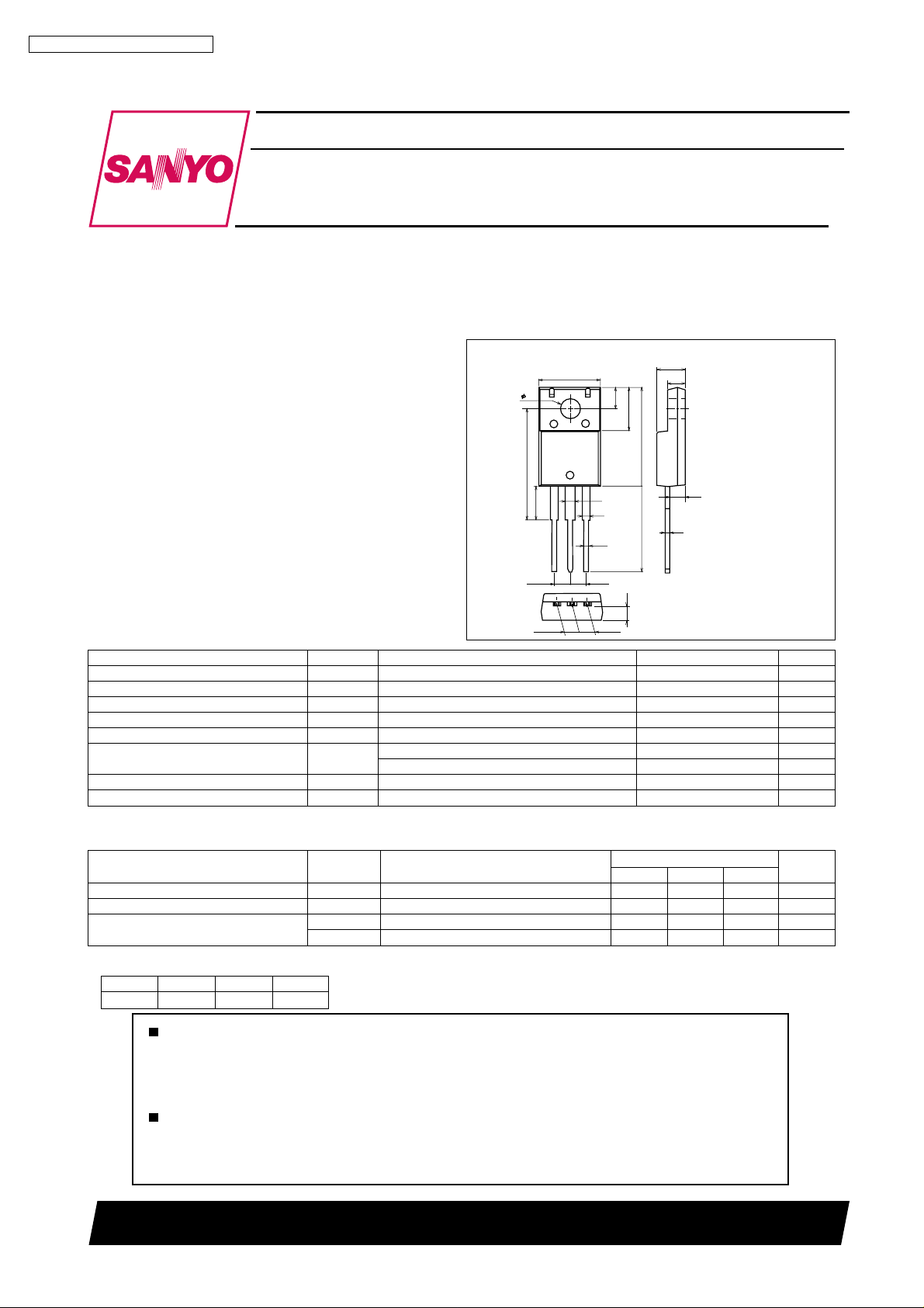
Package Dimensions
unit : mm
2041A
[2SB1133 / 2SD1666]
10.0
3.2
18.1
5.6
1
2.55
2.55
1.6
1.2
0.75
23
2.55
2.55
3.5
7.2
2.4
4.5
2.8
16.0
2.4
0.7
14.0
1 : Base
2 : Collector
3 : Emitter
SANYO : TO-220ML
(−)60 V
(−)60 V
(−)6 V
(−)3 A
(−)8 A
2W
Electrical Characteristics at Ta=25°C
Parameter Symbol Conditions
Collector Cutoff Current I
Emitter Cutoff Current I
DC Current Gain
* : The 2SB1133 / 2SD1666 are classified by 0.5A hFE as follows :
Rank Q R S
h
70 to 140 100 to 200 140 to 280
FE
CBO
EBO
hFE(1) VCE=(--)5V, IC=(--)0.5A *70 *280
hFE(2) VCE=(--)5V, IC=(--)3A 20
VCB=(--)40V, IE=0 (--)100 µA
VEB=(--)4V, IC=0 (--)100 µA
Any and all SANYO products described or contained herein do not have specifications that can handle
applications that require extremely high levels of reliability, such as life-support systems, aircraft's
control systems, or other applications whose failure can be reasonably expected to result in serious
physical and/or material damage. Consult with your SANYO representative nearest you before using
any SANYO products described or contained herein in such applications.
SANYO assumes no responsibility for equipment failures that result from using products at values that
exceed, even momentarily, rated values (such as maximum ratings, operating condition ranges, or other
parameters) listed in products specifications of any and all SANYO products described or contained
herein.
SANYO Electric Co.,Ltd. Semiconductor Company
TOKYO OFFICE Tokyo Bldg., 1-10, 1 Chome, Ueno, Taito-ku, TOKYO, 110-8534 JAPAN
Ratings
min typ max
Continued on next page.
72501 GI IM
Unit
No.3031-1/4
2SB1133 / 2SD1666
Continued from preceding page.
Parameter Symbol Conditions
Gain-Bandwidth Product f
Output Capacitance Cob VCB=(--)10V, f=1MHz (110)60 pF
Collector-to-Emitter Saturation Voltage VCE(sat) IC=(--)2A, IB=(--)0.2A (--)0.6 (--)1 V
Base-to-Emitter Saturation Voltage V
Collector-to-Base Breakdown Voltage V
Collector-to-Emitter Breakdown Voltage V
Emitter-to-Base Breakdown Voltage V
I
-- V
--3.0
--2.5
-- A
--2.0
C
--45mA
--50mA
C
CE
--40mA
BE
(BR)CBOIC
(BR)CEOIC
(BR)EBOIE
--35mA
--30mA
--25mA
--20mA
VCE=(--)5V, IC=(--)0.5A (40)8 MHz
T
VCE=(--)5V, IC=(--)0.5A (--)0.7 (--)1 V
=(--)1mA, IE=0 (--)60 V
=(--)5mA, RBE=∞ (--)60 V
=(--)1mA, IC=0 (--)6 V
3.0
2.5
-- A
2.0
C
45mA
50mA
--15mA
--1.5
1.5
--10mA
--1.0
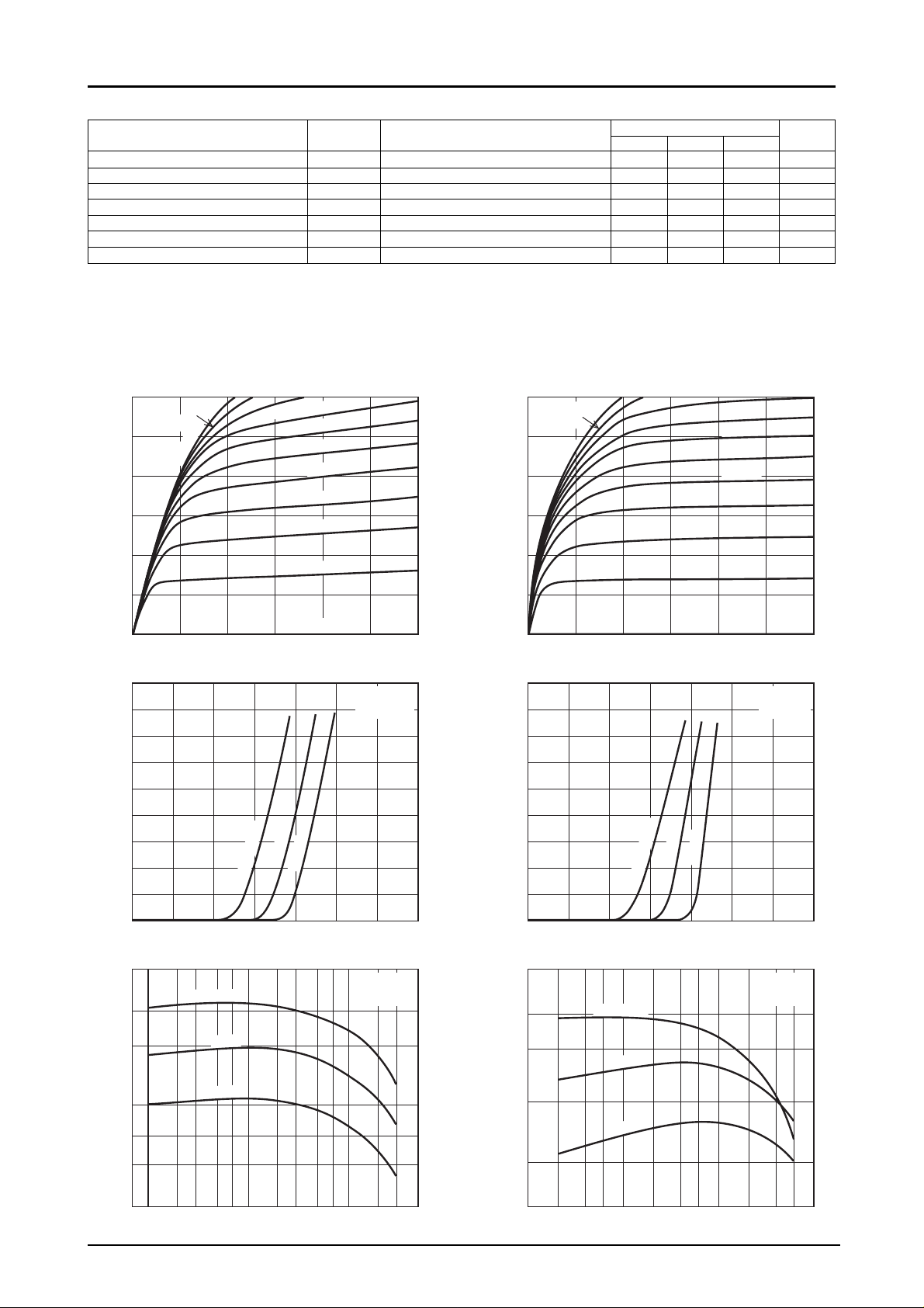
Collector Current, I
--0.5
--5mA
1.0
Collector Current, I
0.5
Ratings
min typ max
I
-- V
C
40mA
CE
35mA
30mA
25mA
20mA
15mA
10mA
5mA
Unit
0
0 --1 --2 --3 --4 --6--5
IB=0
Collector to Emitter Voltage, VCE -- V
I
-- VBE(on)
--3.6
--3.2
--2.8
-- A
--2.6
C
--2.0
--1.6
--1.2
Collector Current, I
--0.8
--0.4
0
0 --0.2 --0.4 --0.6 --0.8 --1.0 --1.2 --1.4
C
°C
Ta=120
°C
°C
25
--40
Base to Emitter On Voltage, VBE(on) -- V
h
-- I
FE
25
FE
°C
°C
5
Ta=120
3
2
C
IT03736
2SB1133
VCE= --5V
IT03738
2SB1133
VCE= --5V
0
0 1.0 2.0 3.0 4.0 6.05.0
IB=0
Collector to Emitter Voltage, VCE -- V
I
-- VBE(on)
3.6
3.2
2.8
-- A
2.6
C
2.0
1.6
1.2
Collector Current, I
0.8
0.4
0
0 0.2 0.4 0.6 0.8 1.0 1.2 1.4
C
°C
Ta=120
°C
°C
25
--40
Base to Emitter On Voltage, VBE(on) -- V
h
-- I
FE
25
FE
°C
°C
5
3
2
Ta=120
C
IT03737
2SD1666
VCE=5V
IT03739
2SD1666
VCE=5V
100
7
DC Current Gain, h
5
3
--0.01
23 57 23 5 23 577
°C
--40
--0.1 --1.0
Collector Current, IC -- A
100
°C
DC Current Gain, h
5
3
IT03740 IT03741
0.01
--40
2355
235 235
0.1
Collector Current, IC -- A
1.0
No.3031-2/4
 Loading...