

Sanyo 2SD1207 Specifications
Ordering number:930C
PNP/NPN Epitaxial Planar Silicon Darlington Transistors
2SB892/2SD1207
Large-Current Switching Applications
Features
· Power supplies, relay drivers, lamp drivers, and
automotive wiring.
Features
· FBET and MBIT processed (Original process of
SANYO).
· Low saturation voltage.
· Large current capacity and wide ASO.
( ) : 2SB892
Specifications
Absolute Maximum Ratings at Ta = 25˚C
retemaraPlobmySsnoitidnoCsgnitaRtinU
egatloVesaB-ot-rotcelloCV
egatloVrettimE-ot-rotcelloCV
egatloVesaB-ot-rettimEV
tnerruCrotcelloCI
)esluP(tnerruCrotcelloCI
noitapissiDrotcelloCelbawollAP
erutarepmeTnoitcnuJjT 051
erutarepmeTegarotSgtsT 051+ot55–
Electrical Characteristics at Ta = 25˚C
retemaraPlobmySsnoitidnoC
tnerruCffotuCrotcelloCI
tnerruCffotuCrettimEI
niaGtnerruCCD
tcudorPhtdiwdnaB-niaGf
ecnaticapaCtuptuOC
* : The 2SB892/2SD1207 are graded as follows by hFE at 100mA :
002R001082S041004T002065U082
OBC
OEC
OBE
C
PC
C
V
OBC
V
OBE
hEF1VECI,V2)–(=
hEF2VECI,V2)–(=
V
T
V
bo
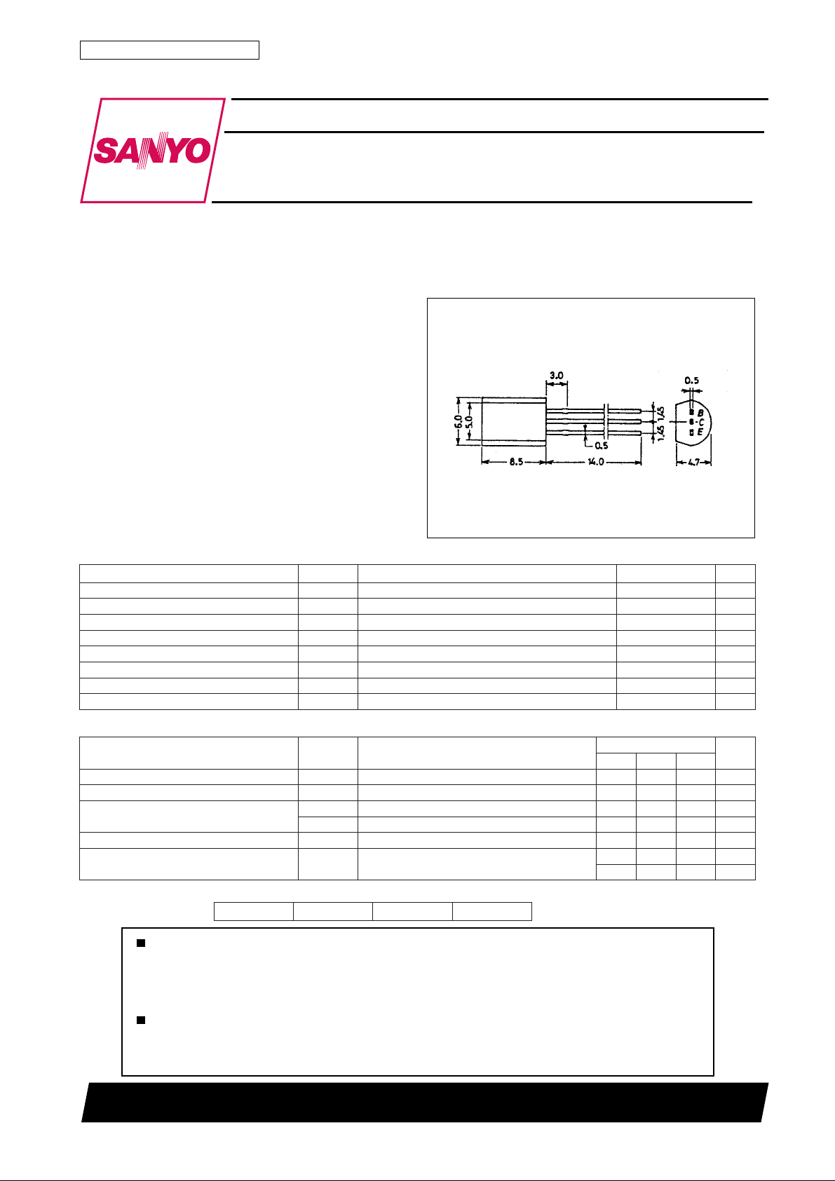
Package Dimensions
unit:mm
2006A
[2SB892/2SD1207]
EIAJ : SC-51 B : Base
SANYO : MP C : Collector
E : Emitter
06)–(V
05)–(V
6)–(V
2)–(A
4)–(A
1W
˚C
˚C
sgnitaR
nimpytxam
I,V05)–(=
BC
BE
EC
BC
0=1.0)–(Aµ
E
I,V4)–(=
0=1.0)–(Aµ
C
C
C
I,V01)–(=
C
Am001)–(=001065
A5.1)–(=04
Am05)–(=051zHM
zHM1=f,V01)–(=
21Fp
)22(Fp
tinU
Any and all SANYO products described or contained herein do not have specifications that can handle
applications that require extremely high levels of reliability, such as life-support systems, aircraft’s
control systems, or other applications whose failure can be reasonably expected to result in serious
physical and/or material damage. Consult with your SANYO representative nearest you before using
any SANYO products described or contained herein in such applications.
SANYO assumes no responsibility for equipment failures that result from using products at values that
exceed, even momentarily, rated values (such as maximum ratings, operating condition ranges,or other
parameters) listed in products specifications of any and all SANYO products described or contained
herein.
SANYO Electric Co.,Ltd. Semiconductor Bussiness Headquaters
TOKYO OFFICE Tokyo Bldg., 1-10, 1 Chome, Ueno, Taito-ku, TOKYO, 110-8534 JAPAN
91098HA (KT)/4067KI/3145KI No.930–1/4

2SB892/2SD1207
retemaraPlobmySsnoitidnoC
egatloVnoitarutaSrettimE-ot-rotcelloCV
egatloVnoitarutaSrettimE-ot-esaBV
egatloVnwodkaerBesaB-ot-rotcelloCV
egatloVnwodkaerBrettimE-ot-rotcelloCV
egatloVnwodkaerBesaB-ot-rettimEV
I
)tas(EC
I
)tas(EB
I
OBC)RB(
I
OEC)RB(
I
OBE)RB(
I,A1)–(=
C
C
C
C
E
B
I,A1)–(=
B
Am05)–(=
Am05)–(=9.0)–(2.1)–(V
I,Aµ01)–(=
0=06)–(V
E
R,Am1)–(=
=∞ 05)–(V
EB
I,Aµ01)–(=
0=6)–(V
C
sgnitaR
nimpytxam
51.04.0V
)3.0–()7.0–(V
tinU
No.930–2/4
 Loading...