

Sanyo 2SC5764 Specifications
Ordering number : ENN6971A
2SC5764
NPN Triple Diffused Planar Silicon Transistor
2SC5764
Switching Regulator Applications
Features
•
High breakdown voltage.
• High reliability.
• High-speed switching.
• Wide ASO.
• Adoption of MBIT process.
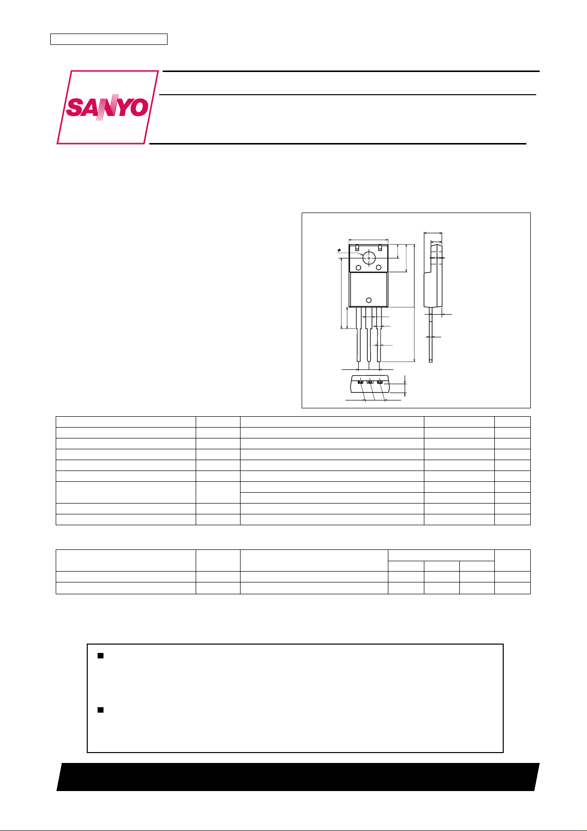
Package Dimensions
unit : mm
2041A
[2SC5764]
10.0
3.2
18.1
5.6
1
2.55
1.6
23
2.55
1.2
0.75
3.5
7.2
2.4
16.0
14.0
4.5
2.8
2.4
0.7
1 : Base
2 : Collector
3 : Emitter
Specifications
Absolute Maximum Ratings at T a=25°C
Parameter Symbol Conditions Ratings Unit
Collector-to-Base Voltage V
Collector-to-Emitter Voltage V
Emitter-to-Base Voltage V
Collector Current I
Collector Current (Pulse) I
Collector Dissipation P
Junction T emperature Tj 150 ° C
Storage T emperature T stg --55 to +150 °C
CBO
CEO
EBO
C
CP
C
PW≤300µs, Duty cycle≤10% 14 A
Tc=25°C30W
2.55
2.55
SANYO : TO-220ML
700 V
400 V
8V
7A
2.0 W
Electrical Characteristics at Ta=25°C
Parameter Symbol Conditions
Collector Cutoff Current I
Emitter Cutoff Current I
CBO
EBO
Any and all SANYO products described or contained herein do not have specifications that can handle
applications that require extremely high levels of reliability, such as life-support systems, aircraft's
control systems, or other applications whose failure can be reasonably expected to result in serious
physical and/or material damage. Consult with your SANYO representative nearest you before using
any SANYO products described or contained herein in such applications.
SANYO assumes no responsibility for equipment failures that result from using products at values that
exceed, even momentarily, rated values (such as maximum ratings, operating condition ranges, or other
parameters) listed in products specifications of any and all SANYO products described or contained
herein.
SANYO Electric Co.,Ltd. Semiconductor Company
TOKYO OFFICE Tokyo Bldg., 1-10, 1 Chome, Ueno, Taito-ku, TOKYO, 110-8534 JAPAN
Ratings
min typ max
VCB=400V, IE=0 10 µA
VEB=5V, IC=0 10 µA
Unit
Continued on next page.
D0301 TS IM TA-3502 / 92001 TS IM TA-3235
No.6971-1/4
2SC5764
Continued from preceding page.
Parameter Symbol Conditions
hFE1VCE=5V, IC=0.8A 20* 50*
DC Current Gain hFE2VCE=5V, IC=4A 10
hFE3VCE=5V, IC=1mA 10
Collectoe-to-Emitter Saturation Voltage VCE(sat) IC=4A, IB=0.8A 0.8 V
Base-to-Emitter Saturation Voltage VBE(sat) IC=4A, IB=0.8A 1.5 V
Gain-Bandwidth Product f
Output Capacitance Cob VCB=10V , f=1MHz 80 pF
Collector-to-Base Breakdown Voltage V
Collector-to-Emitter Breakdown Voltage V
Emitter-to-Base Breakdown Voltage V
Turn-On Time t
Storage Time t
Fall Time t
* : The 2SC5764 is classified by 0.8A hFE as follows.
Rank M N
h
FE
20 to 40 30 to 50
(BR)CBOIC
(BR)CEOIC
(BR)EBOIE
on
stg
VCE=10V, IC=0.8A 17 MHz
T
=1mA, IE=0 700 V
=5mA, RBE=∞ 400 V
=1mA, IC=0 8 V
IC=5A, IB1=1A, IB2=--2A, RL=40Ω, VCC=200V
IC=5A, IB1=1A, IB2=--2A, RL=40Ω, VCC=200V
IC=5A, IB1=1A, IB2=--2A, RL=40Ω, VCC=200V
f
min typ max
Ratings
0.5 µs
2.5 µs
0.25 µs
Unit
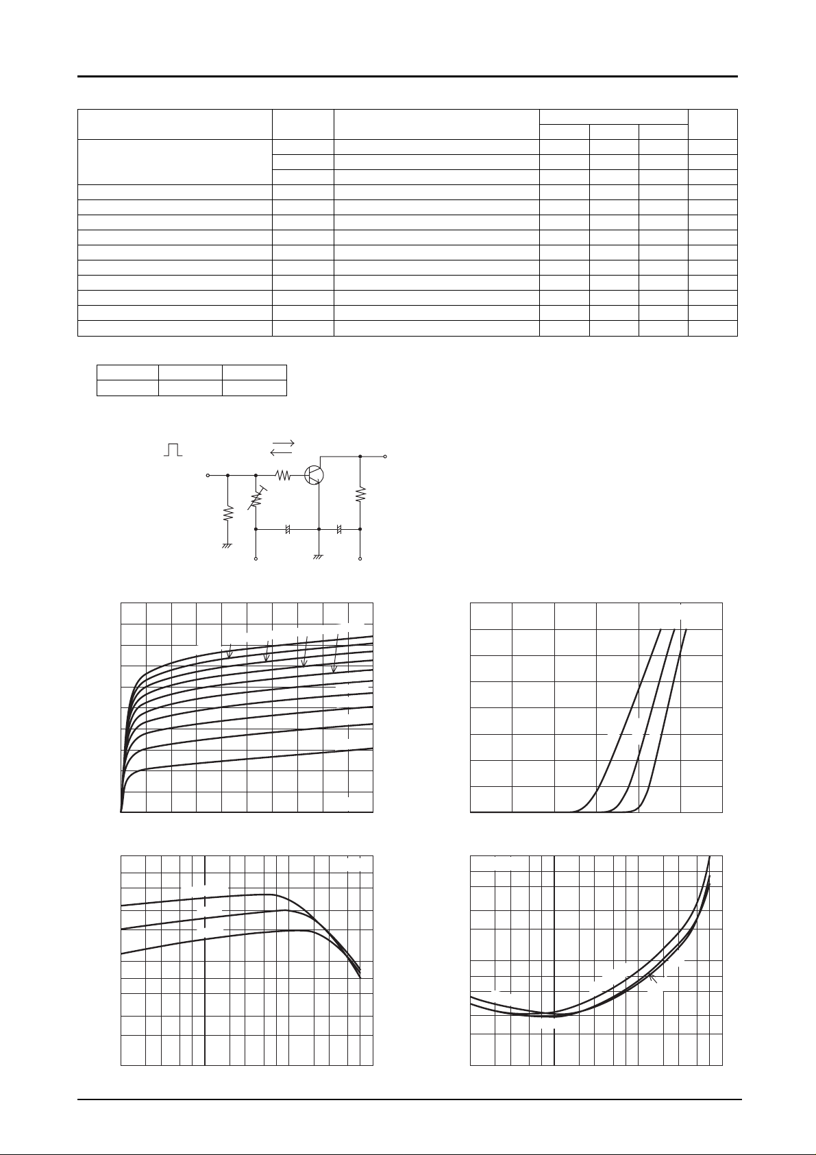
Switching Time Test Circuit
PW=20µs
D.C.≤1%
INPUT
V
R
50Ω
1000mA
Ta=120
25
--40
IC -- V
h
FE
°C
°C
°C
900mA
10
8
-- A
C
6
4
Collector Current, I
2
0
0
Collector-to-Emitter Voltage, VCE -- V
100
7
5
3
FE
2
10
7
5
DC Current Gain, h
3
2
246810
I
B1
I
B2
R
B
100µF 470µF
CE
800mA
-- I
C
+
700mA
OUTPUT
R
L
+
VCC=200VVBE= --5V
IC -- V
8
600mA
500mA
400mA
300mA
7
6
-- A
C
5
4
200mA
100mA
3
2
Collector Current, I
1
=0
I
B
IT03053 IT03054
VCE=5V
0
0 0.2 0.4 0.6 0.8 1.0 1.2
Base-to-Emitter V oltage, VBE -- V
1.0
IC / IB=5
7
5
3
(sat) -- V
2
VCE(sat) -- I
BE
Ta=120
VCE=5V
°C
°C
°C
25
--40
C
CE
0.1
7
5
3
2
Collector-to-Emitter
Saturation V oltage, V
--40
°C
25
Ta=120°C
°C
25
--40
°C
°C
1.0
23 752375
0.01
23 75
0.1
Collector Current, IC -- A
1.0
10
IT03055
0.01
23 752375
0.01
23 75
0.1
1.0
Collector Current, IC -- A
10
IT03056
No.6971-2/4
 Loading...