

SANYO 2SC5706, 2SA2039 Datasheet
Ordering number : ENN6912
2SA2039 / 2SC5706
PNP / NPN Epitaxial Planar Silicon Transistors
2SA2039 / 2SC5706
High Current Switching Applications
Features
•
DC-DC converter, relay drivers, lamp drivers,
motor drivers, strobes.
Features
• Adoption of FBET, MBIT process.
•
Large current capacitance.
• Low collector-to-emitter saturation voltage.
• High-speed switching.
• High allowable power dissipation.
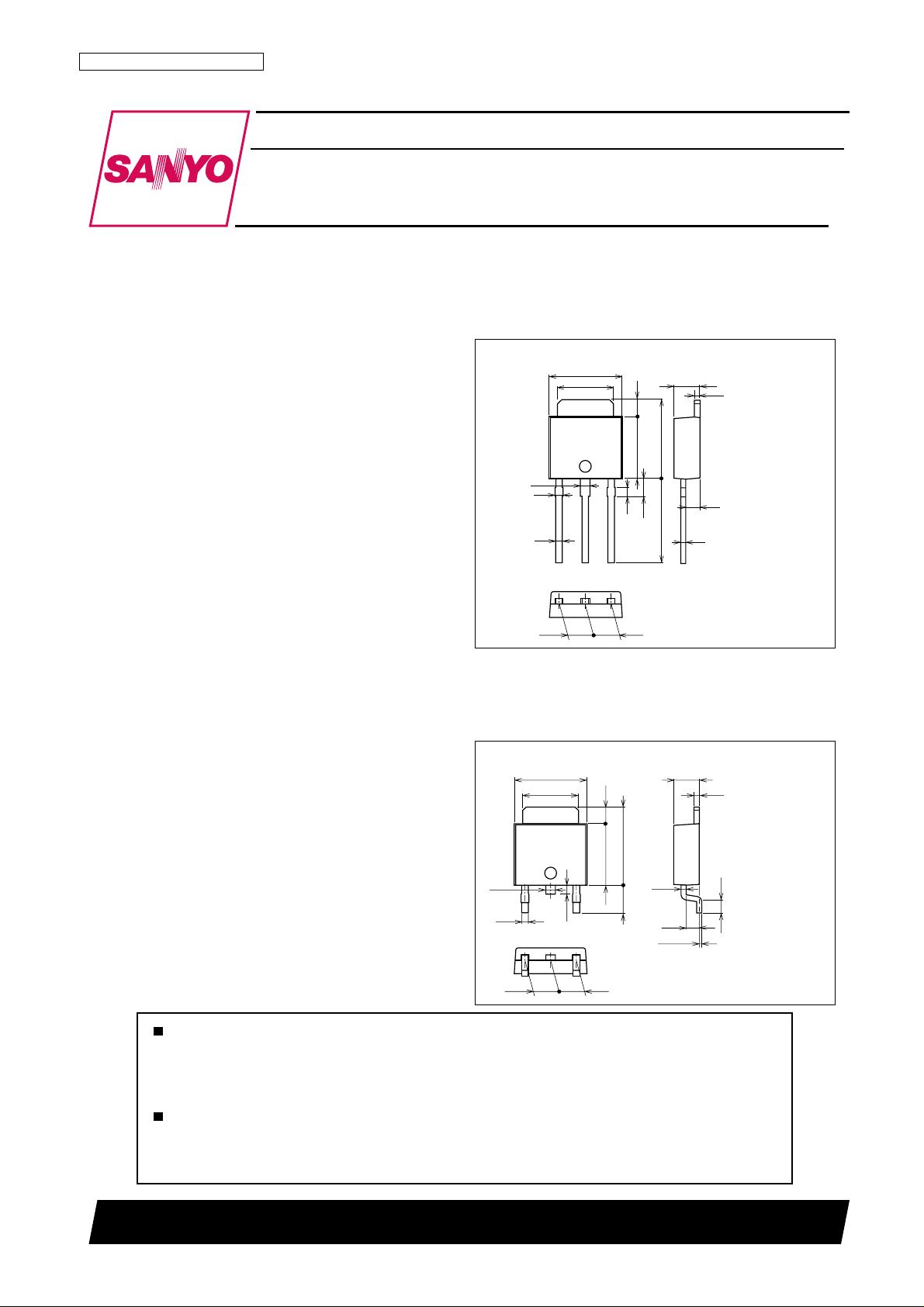
Package Dimensions
unit : mm
2045B
[2SA2039 / 2SC5706]
6.5
5.0
4
0.85
0.7
0.6
1
23
2.3 2.3
0.8
1.5
5.5
1.6
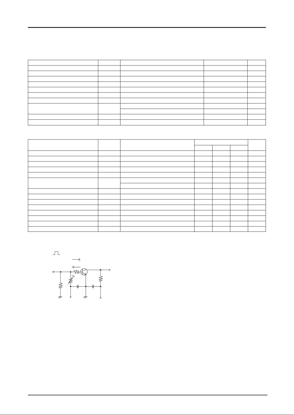
Package Dimensions
unit : mm
2044B
7.0
7.5
2.3
0.5
0.5
1.2
1 : Base
2 : Collector
3 : Emitter
4 : Collector
SANYO : TP
[2SA2039 / 2SC5706]
6.5
5.0
4
0.85
12
0.6
2.3 2.3
0.8
3
1.55.5
7.0
2.5
0.5
1.2
0 to 0.2
2.3
0.5
1.2
1 : Base
2 : Collector
3 : Emitter
4 : Collector
SANYO : TP-FA
Any and all SANYO products described or contained herein do not have specifications that can handle
applications that require extremely high levels of reliability, such as life-support systems, aircraft's
control systems, or other applications whose failure can be reasonably expected to result in serious
physical and/or material damage. Consult with your SANYO representative nearest you before using
any SANYO products described or contained herein in such applications.
SANYO assumes no responsibility for equipment failures that result from using products at values that
exceed, even momentarily, rated values (such as maximum ratings, operating condition ranges, or other
parameters) listed in products specifications of any and all SANYO products described or contained
herein.
SANYO Electric Co.,Ltd. Semiconductor Company
TOKYO OFFICE Tokyo Bldg., 1-10, 1 Chome, Ueno, Taito-ku, TOKYO, 110-8534 JAPAN
30101 TS IM TA-3232
No.6912-1/5
2SA2039 / 2SC5706
Specifications
Note*( ) : 2SA2039
Absolute Maximum Ratings at Ta=25°C
Parameter Symbol Conditions Ratings Unit
Collector-to-Base Voltage V
Collector-to-Emitter Voltage V
Collector-to-Emitter Voltage V
Emitter-to-Base Voltage V
Collector Current I
Collector Current (Pulse) I
Base Current I
Collector Dissipation P
Junction T emperature Tj 150 °C
Storage T emperature T stg --55 to +150 °C
CBO
CES
CEO
EBO
C
CP
B
C
Tc=25°C15W
Electrical Characteristics at Ta=25°C
(--50)80 V
(--50)80 V
(--)50 V
(--)6 V
(--)5 A
(--)7.5 A
(--)1.2 A
0.8 W
Parameter Symbol Conditions
Collector Cutoff Current I
Emitter Cutoff Current I
DC Current Gain h
Gain-Bandwidth Product f
Output Capacitance Cob VCB=(--)10V, f=1MHz (24)15 pF
Collector-to-Emitter Saturation Voltage VCE(sat)
Base-to-Emitter Saturation Voltage VBE(sat) IC=(--)2A, IB=(--)100mA (--)0.89 (--)1.2 V
Collector-to-Base Breakdown Voltage V
Collector-to-Emitter Breakdown Voltage V
Collector-to-Emitter Breakdown Voltage V
Emitter-to-Base Breakdown Voltage V
Turn-On Time t
Storage Time t
Fall Time t
CBO
EBO
FE
(BR)CBOIC
(BR)CESIC
(BR)CEOIC
(BR)EBOIE
on
stg
VCB=(--)40V, IE=0 (--)1 µA
VEB=(--)4V, IC=0 (--)1 µA
VCE=(--)2V, IC=(--)500mA 200 560
VCE=(--)10V, IC=(--)500mA (360)400 MHz
T
IC=(--)1A, IB=(--)50mA
IC=(--)2A, IB=(--)100mA
=(--)10µA, IE=0 (--50)80 V
=(--)100µA, RBE=0 (--50)80 V
=(--)1mA, RBE=∞ (--)50 V
=(--)10µA, IC=0 (--)6 V
See specified test circuit.
See specified test circuit.
See specified test circuit.
f
min typ max
Ratings
(--115)90 (--195)135
(--255)160 (--430)240
(30)35
(230)300
(15)20
Swicthing Time Test Circuit
I
VR10
B1
I
B2
R
B
+
100µF 470µF
OUTPUT
25Ω
+
PW=20µs
D.C.≤1%
INPUT
50Ω
Unit
mV
mV
ns
ns
ns
VBE= --5V
10IB1= --10IB2= IC=1A
For PNP, the polarity is reversed.
VCC=25V
No.6912-2/5
 Loading...