

Sanyo 2SC5450 Specifications
Any and all SANYO products described or contained herein do not have specifications that can handle
applications that require extremely high levels of reliability, such as life-support systems, aircraft’s
control systems, or other applications whose failure can be reasonably expected to result in serious
physical and/or material damage. Consult with your SANYO representative nearest you before using
any SANYO products described or contained herein in such applications.
SANYO assumes no responsibility for equipment failures that result from using products at values that
exceed, even momentarily, rated values (such as maximum ratings, operating condition ranges,or other
parameters) listed in products specifications of any and all SANYO products described or contained
herein.
NPN Triple Diffused Planar Silicon Transistor
Ultrahigh-Definition CRT Display
Horizontal Deflection Output Applications
Ordering number:EN5955
2SC5450
SANYO Electric Co.,Ltd. Semiconductor Company
TOKYO OFFICE Tokyo Bldg., 1-10, 1 Chome, Ueno, Taito-ku, TOKYO, 110-8534 JAPAN
16.0
Features
· High speed.
· High breakdown voltage (V
CBO
=1600V).
· High reliability (Adoption of HVP process).
· Adoption of MBIT process.
Specifications
Absolute Maximum Ratings at Ta = 25˚C
retemaraPlobmySsnoitidnoCsgnitaRtinU
egatloVesaB-ot-rotcelloCV
egatloVrettimE-ot-rotcelloCV
egatloVesaB-ot-rettimEV
tnerruCrotcelloCI
)esluP(tnerruCrotcelloCI
noitapissiDrotcelloCP
erutarepmeTnoitcnuJjT 051
erutarepmeTegarotSgtsT 051+ot55–
C
C
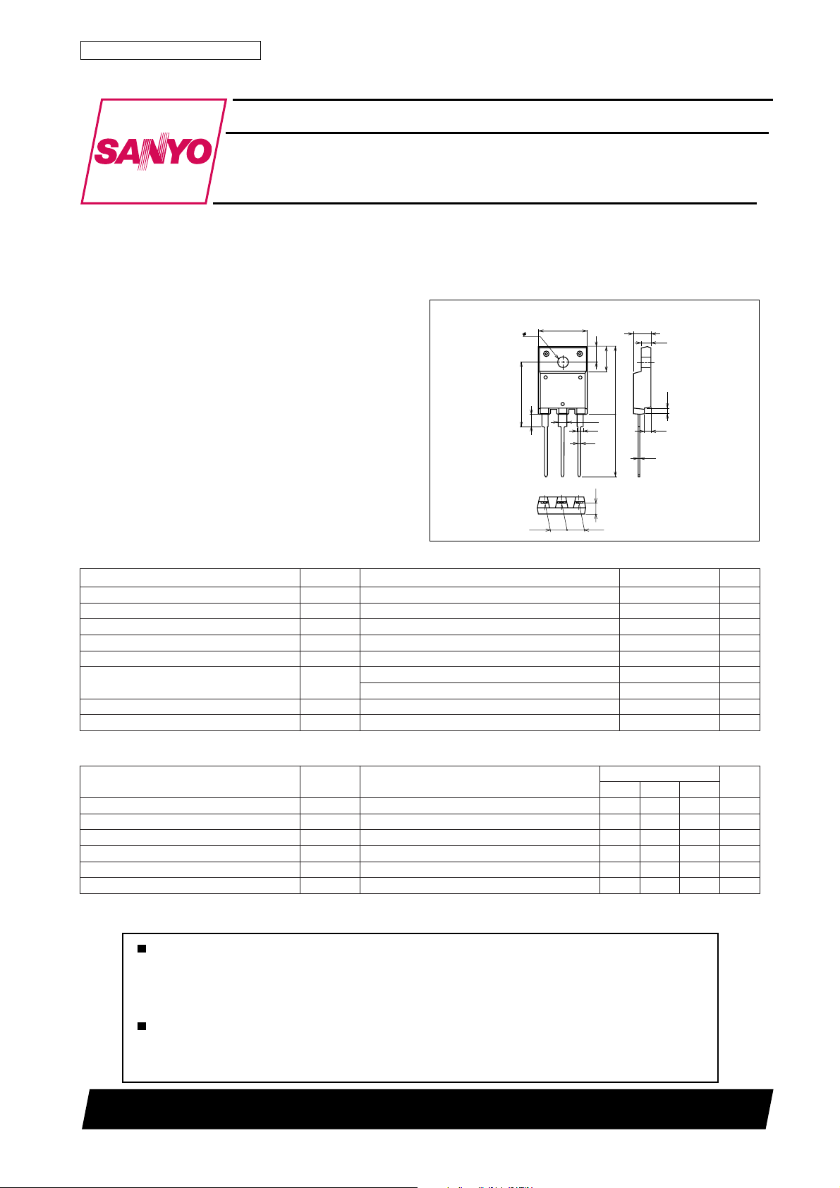
Package Dimensions
unit:mm
2039D
[2SC5450]
3.4
21.0
4.0
12
5.45
OBC
OEC
OBE
PC
Tc=25˚C
2.8
2.0
1.0
3
3.5
5.45
5.6
3.1
5.0
8.0
22.0
2.0
2.0
20.4
0.6
1 : Base
2 : Collector
3 : Emitter
SANYO : TO-3PML
0061V
008V
6V
01A
52A
0.3W
07W
˚C
˚C
Electrical Characteristics at Ta = 25˚C
retemaraPlobmySsnoitidnoC
tnerruCffotuCrotcelloC
tnerruCffotuCrotcelloC
egatloVniatsuSrettimE-ot-rotcelloCV
tnerruCffotuCrettimEI
egatloVnoitarutaSrettimE-ot-rotcelloCV
egatloVnoitarutaSrettimE-ot-esaBV
I
I
V
OBC
V
SEC
I
)sus(OEC
C
V
OBE
I
)tas(EC
C
I
)tas(EB
C
I,V008=
BC
EC
BE
0=01Aµ
E
R,V0061=
0=0.1Am
EB
I,Am001=
0=008V
B
I,V4=
0=0.1Am
C
I,A7=
A57.1=
B
I,A7=
A57.1=5.1V
B
sgnitaR
nimpytxam
tinU
5V
Continued on next page.
61099TS (KOTO) TA-1386 No.5957–1/4
2SC5450
Continued from preceding page.
retemaraPlobmySsnoitidnoC
niaGtnerruCCD
emiTegarotSt
emiTllaFt
hEF1VECI,V5=
hEF2VECI,V5=
I
gts
C
I
f
C
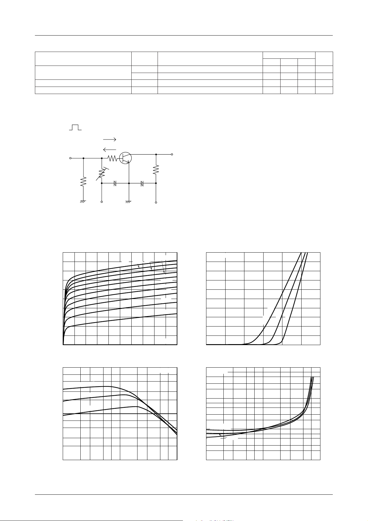
Switching Time Test Circuit
A1=
C
A7=
C
I,A6=
I,A6=
I,A0.1=
1B
1B
2B
I,A0.1=
2B
sgnitaR
nimpytxam
5103
47
A5.2–=
A5.2–=
tinU
0.3sµ
2.0sµ
PW=20µs
D.C.≤1%
INPUT
50Ω
10
9
8
7
–A
C
6
5
4
3
Collector Current, I
2
1
0
024681013579
V
R
VBE=–2V
I
B1
I
B2
R
100µF
IC-
OUTPUT
B
+
470µF
V
CE
1.8A
2.0A
+
VCC=200V
1.6A
RL=33.3Ω
1.4A
1.2A
1.0A
0.8A
0.6A
0.4A
0.2A
I
B
Collector-to-Emitter Voltage, VCE–V
10
VCE=5V
9
8
–A
7
C
6
5
4
3
Collector Current, I
2
=
0
1
0
0 0.2 0.4 0.6 0.8 1.0 1.2
IC-
V
Ta=120°C
BE
25°C
40°C
-
Base-to-Emitter Voltage, VBE–V
100
7
5
Ta=120°C
3
FE
2
10
7
5
DC Current Gain, h
3
2
1.0
0.1
25°C
40°C
-
2357
hFE-
357
Collector Current, IC– A Collector Current, IC–A
I
C
VCE=5V
2
1.0
10
10
I
/
IB=5
C
7
5
3
–V
2
1.0
CE(sat)
7
5
3
2
40°C
-
Ta=
0.1
7
5
120°C
Collector-to-Emitter
Saturation Voltage, V
3
2
0.01
2357
0.1
V
CE(sat
25°C
357
-
I
)
C
1.0
2
10
No.5955–2/4
 Loading...