

Sanyo 2SC5347 Specifications
SANYO Electric Co.,Ltd. Semiconductor Bussiness Headquaters
TOKYO OFFICE Tokyo Bldg., 1-10, 1 Chome, Ueno, Taito-ku, TOKYO, 110-8534 JAPAN
Any and all SANYO products described or contained herein do not have specifications that can handle
applications that require extremely high levels of reliability, such as life-support systems, aircraft’s
control systems, or other applications whose failure can be reasonably expected to result in serious
physical and/or material damage. Consult with your SANYO representative nearest you before using
any SANYO products described or contained herein in such applications.
SANYO assumes no responsibility for equipment failures that result from using products at values that
exceed, even momentarily, rated values (such as maximum ratings, operating condition ranges,or other
parameters) listed in products specifications of any and all SANYO products described or contained
herein.
NPN Epitaxial Planar Silicon Transistor
High-Frequency Semi-Power Output Stage,
Low-Noise Medium Output Amplifiers Applications
Ordering number:EN5512A
2SC5347
4.5
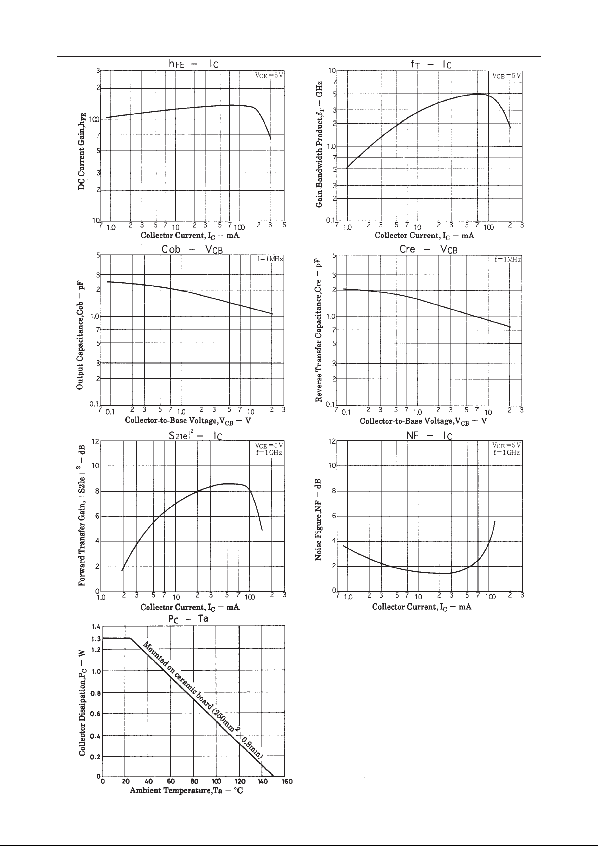
Features
· High frequency medium output amplification
(VCE=5V, IC=50mA)
: fT=4.7GHz typ (f=1GHz).
: S21e2=8dB typ (f=1GHz).
: NF=1.8dB typ (f=1GHz).
Specifications
Absolute Maximum Ratings at Ta = 25˚C
retemaraPlobmySsnoitidnoCsgnitaRtinU
egatloVesaB-ot-rotcelloCV
egatloVrettimE-ot-rotcelloCV
egatloVesaB-ot-rettimEV
tnerruCrotcelloCI
noitapissiDrotcelloCP
erutarepmeTnoitcnuJjT 051
erutarepmeTegarotSgtsT 051+ot55–
Electrical Characteristics at Ta = 25˚C
retemaraPlobmySsnoitidnoC
tnerruCffotuCrotcelloCI
tnerruCffotuCrettimEI
niaGtnerruCCD
tcudorPhtdiwdnaB-niaG
ecnaticapaCtuptuOboCV
ecnaticapaCrefsnarTesreveRerCV
niaGrefsnarTdrawroF
erugiFesioN
* : The 2SC5347 is classified by 50mA hFE as follows :
Marking : CZ
hFE rank : D, E, F
C
C
h
EF
f
T
FNVECI,V5=
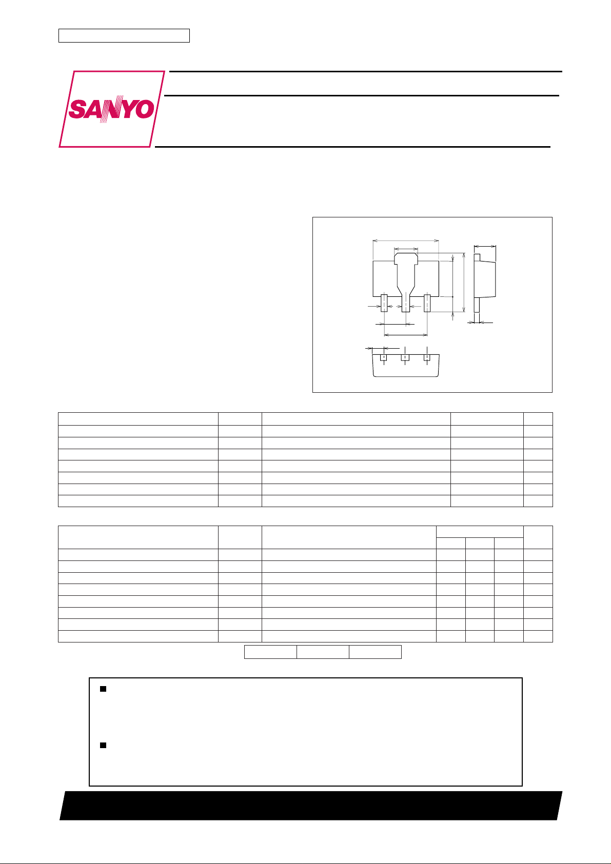
Package Dimensions
unit:mm
2038A
[2SC5347]
1.6
0.4
OBC
OEC
OBE
2
mm052(draobcimarecnodetnuoM
× )mm8.03.1W
V
OBC
V
OBE
V
V
2
V
|e12S|
I,V01=
BC
BE
EC
EC
BC
BC
EC
0=0.1Aµ
E
I,V1=
0=01Aµ
C
I,V5=
C
I,V5=
C
I,V5=
C
C
021D06081E09072F531
Am05=
Am05=
zHM1=f,V01=
zHM1=f,V01=
zHG1=f,Am05=
zHG1=f,Am05=8.10.3Bd
0.5
3
1.5
0.75
1
2
3.0
1.5
2.5
4.25max
1.0
0.4
1 : Base
2 : Collector
3 : Emitter
SANYO : PCP
(Bottom view)
sgnitaR
nimpytxam
*06*072
37.4zHG
3.10.2Fp
9.0Fp
68 Bd
02V
21V
2V
051Am
˚C
˚C
tinU
21599TH (KT)/91296YK (KOTO) TA-0689 No.5512–1/5
2SC5347
No.5512–2/5
 Loading...