

SANYO 2SC5291 Datasheet

Ordering number : ENN5282A
2SC5291
NPN Epitaxial Planar Silicon Transistor
2SC5291
High-Voltage Switching Applications
Features
• Adoption of FBET, MBIT processes.
• Large current capacity.
• Can be provided in taping.
• 9.5mm onboard mounting height.
Package Dimensions
unit : mm
2084B
[2SC5291]
10.5
1.0
1.2
0.5
123
1.6
8.5
7.5
1.9
1.2
4.5
0.5
2.6
1.4
1 : Emitter
2 : Collector
Specifications
Absolute Maximum Ratings at Ta=25°C
Parameter Symbol Conditions Ratings Unit
Collector-to-Base Voltage V
Collector-to-Emitter Voltage V
Emitter-to-Base Voltage V
Collector Current I
Collector Current (Pulse) I
Base Current I
Collector Dissipation P
Junction T emperature Tj 150 ° C
Storage T emperature T stg --55 to +150 °C
CBO
CEO
EBO
C
CP
B
C
2.5 2.5
3 : Base
SANYO : FLP
180 V
160 V
6V
1.5 A
2.5 A
300 mA
1.5 W
Electrical Characteristics at Ta=25°C
Parameter Symbol Conditions
Collector Cutoff Current I
Emitter Cutoff Current I
CBO
EBO
Any and all SANYO products described or contained herein do not have specifications that can handle
applications that require extremely high levels of reliability, such as life-support systems, aircraft's
control systems, or other applications whose failure can be reasonably expected to result in serious
physical and/or material damage. Consult with your SANYO representative nearest you before using
any SANYO products described or contained herein in such applications.
SANYO assumes no responsibility for equipment failures that result from using products at values that
exceed, even momentarily, rated values (such as maximum ratings, operating condition ranges, or other
parameters) listed in products specifications of any and all SANYO products described or contained
herein.
SANYO Electric Co.,Ltd. Semiconductor Company
TOKYO OFFICE Tokyo Bldg., 1-10, 1 Chome, Ueno, Taito-ku, TOKYO, 110-8534 JAPAN
Ratings
min typ max
VCB=120V, IE=0 1.0 µA
VEB=4V, IC=0 1.0 µA
Unit
Continued on next page.
12201 TS IM TA-0376
No.5282-1/4
2SC5291
Continued from preceding page.
Parameter Symbol Conditions
DC Current Gain
Gain-Bandwidth Product f
Output Capacitance Cob VCB=10V, f=1MHz 14 pF
Collector-to-Emitter Saturation Voltage VCE(sat) IC=500mA, IB=50mA 0.13 0.45 V
Base-to-Emitter Saturation Voltage VBE(sat) IC=500mA, IB=50mA 0.85 1.2 V
Turn-ON Time t
Storage Time t
Fall Time t
* : The 2SC5291 is classified by 100mA hFE as follows :
Rank R S T
h
100 to 200 140 to 280 200 to 400
FE
hFE1VCE=5V, IC=100mA 100 400
hFE2VCE=5V, IC=10mA 90
VCE=10V , IC=50mA 120 MHz
T
on
stg
See specified Test Circuit 4.0 ns
See specified Test Circuit 1.2 µs
See specified Test Circuit 8.0 ns
f
min typ max
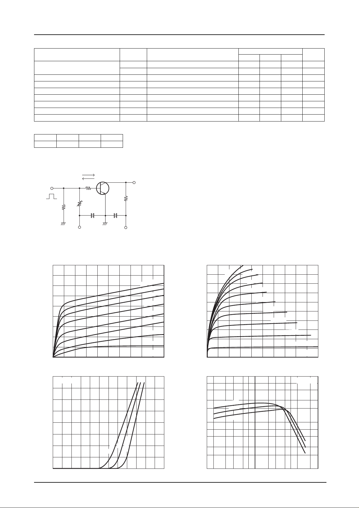
Switching Time Test Circuit
I
B1
I
R
V
R
VBE= --5V
B2
B
+
100µF 470µF
INPUT
PW=20µs
D.C.=≤1%
50Ω
10IB1=--10IB2=IC=700mA
RL=140Ω, RB=14Ω at IC=700mA
OUTPUT
R
L
+
VCC=100V
Ratings
Unit
1.8
1.6
1.4
A
--
1.2
C
1.0
0.8
0.6
Collector Current, I
0.4
0.2
0
012345
IC -- V
Collector-to-Emitter Voltage, V
1.6
VCE=5V
A
1.2
--
IC -- V
CE
BE
50mA
40mA
30mA
20mA
10mA
5mA
2mA
1mA
=0
I
B
ITR08045
V Collector-to-Emitter Voltage, V
CE --
C
0.8
0.4
Collector Current, I
Ta=75°C
25°C
--25°C
4.5mA
4.0mA
IC -- V
3.5mA
1.0
0.8
A
-C
0.6
5.0mA
CE
3.0mA
2.5mA
2.0mA
0.4
Collector Current, I
0.2
1.5mA
1.0mA
0.5mA
=0
I
0
01020304050
CE --
1000
7
5
3
FE
100
DC Current Gain, h
Ta=75°C
2
7
5
3
2
hFE -- I
25°C
--25°C
C
B
ITR08046
V
VCE=5V
0
0 0.2 0.4 0.6 0.8 1.0 1.2
Base-to-Emitter V oltage, VBE -- V
ITR08047
10
72
0.01
2
35
72
0.1
Collector Current, I
35 3
7
1.0
C --
A
ITR08048
No.5282-2/4
 Loading...