

Page 1
Ordering number : ENN3184A
2SC4432
NPN Epitaxial Planar Silicon Transistor
2SC4432
High-Frequency
General-Purpose Amplifier Applications
Features
•
High power gain.
•
High cutoff frequency.
•
Small Cob, Cre.
•
Ultrasmall-sized package permitting the 2SC4432applied sets to be made small and slim.
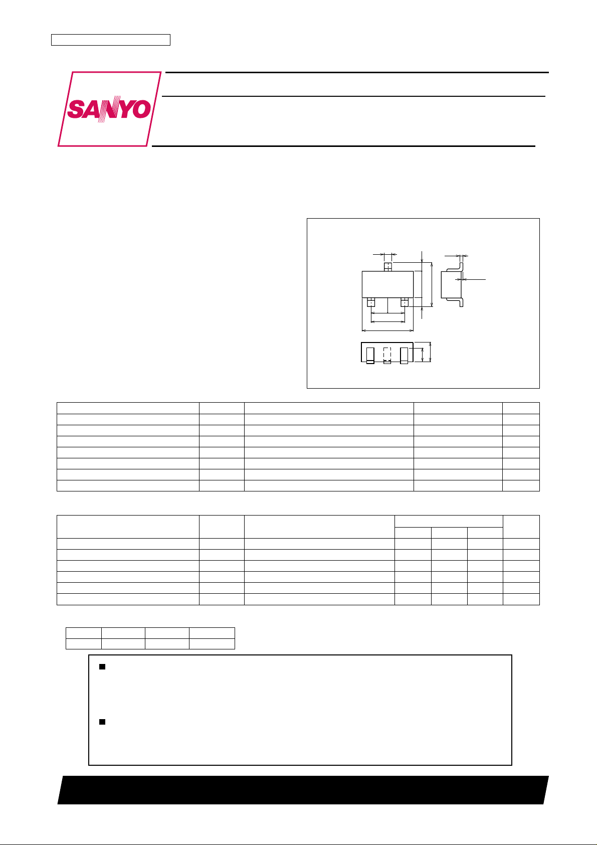
Package Dimensions
unit : mm
2018B
[2SC4432]
0.4
3
0.95
0.95
1
2
1.9
2.9
0.5
2.5
1.5
0.5
1.1
0.8
0.16
0 to 0.1
1 : Base
2 : Emitter
3 : Collector
SANYO : CP
Specifications
Absolute Maximum Ratings at T a=25°C
Parameter Symbol Conditions Ratings Unit
Collector-to-Base Voltage V
Collector-to-Emitter Voltage V
Emitter-to-Base Voltage V
Collector Current I
Collector Dissipation P
Junction T emperature Tj 150 °C
Storage T emperature T stg --55 to +150 °C
CBO
CEO
EBO
C
C
40 V
18 V
3V
50 mA
250 mW
Electrical Characteristics at Ta=25°C
Parameter Symbol Conditions
Collector Cutoff Current I
Emitter Cutoff Current I
DC Current Gain h
Gain-Bandwidth Product f
Output Capacitance Cob VCB=10V , f=1MHz 0.7 1.2 pF
Reverse Transfer Capacitance Cre VCB=10V , f=1MHz 0.45 pF
Marking : RT Continued on next page.
* : The 2SC4432 is classified by 5mA h
Rank 3 4 5
h
60 to 120 90 to 180 135 to 270
FE
FE
CBO
EBO
FE
as follows :
VCB=18V, IE=0 0.1 µA
VEB=2V, IC=0 0.1 µA
VCE=10V, IC=5mA 60* 270*
VCE=10V, IC=5mA 750 MHz
T
Any and all SANYO products described or contained herein do not have specifications that can handle
applications that require extremely high levels of reliability, such as life-support systems, aircraft's
control systems, or other applications whose failure can be reasonably expected to result in serious
physical and/or material damage. Consult with your SANYO representative nearest you before using
any SANYO products described or contained herein in such applications.
SANYO assumes no responsibility for equipment failures that result from using products at values that
exceed, even momentarily, rated values (such as maximum ratings, operating condition ranges, or other
parameters) listed in products specifications of any and all SANYO products described or contained
herein.
Ratings
min typ max
Unit
SANYO Electric Co.,Ltd. Semiconductor Company
TOKYO OFFICE Tokyo Bldg., 1-10, 1 Chome, Ueno, Taito-ku, TOKYO, 110-8534 JAPAN
D2001 TS IM / D1598 HA (KT) / 7219 YT, TS
No.3184-1/3
Page 2
2SC4432
Continued from preceding page.
Parameter Symbol Conditions
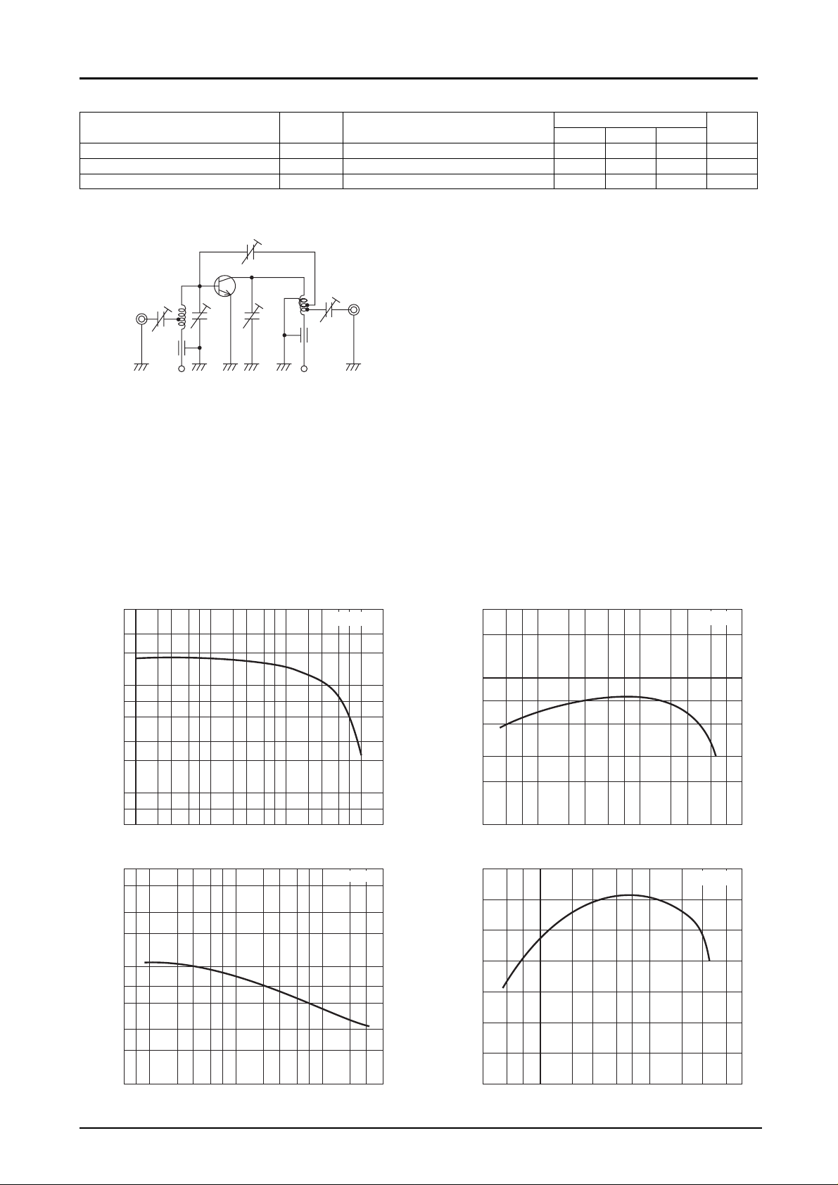
Collector-to-Emitter Saturation Voltage VCE(sat) IC=10mA, IB=1mA 0.2 V
Base-to-Collector Time Constant rbb’C
Power Gain PG VCE=10V, IC=10mA, f=100MHz 28 dB
VCE=10V, IC=5mA, f=31.9MHz 23 ps
C
PG Test Circuit
to 5pF
Ratings
min typ max
Unit
50Ω
to 30pF
1000pF
L1
to 22pF to 22pF
V
B
input
L1 : 1mmφ plated wire, 10mmφ 5T, pitch 15mm,
tap : 2T from base side
L2 : 1mmφ plated wire, 10mmφ 7T, pitch 10mm,
tap : 2T from VC side
L3 : 1mmφ enamel wire, 10mmφ 3T, pitch 10mm
h
-- I
5
3
2
FE
100
7
5
3
2
DC Current Gain, h
10
7
5
2537102537 2 2537
FE
1.00.1
Collector Current, I
Cre -- V
-- pF
7
5
3
2
1.0
7
5
3
2
Reverse Transfer Capacitance, Cre
0.1
75
2537 2 53
0.1
2537
Collector-to-Base Voltage, V
C
C
CB
1000pF
V
C
-- mA
CB
L3
to 30pF
VCE=10V
101.0
-- V
output
50Ω
100
ITR06895
f=1MHz
ITR06897
3
2
-- MHz
T
1000
7
5
3
2
Gain-Bandwidth Product, f
100
75
Collector Current, IC -- mA
30
28
26
-- dB
24
22
20
Power Gain, PG
18
16
7523
Collector Current, IC -- mA
f
-- I
T
C
VCE=10V
25337
PG -- I
25377
101.0
100
ITR06896
C
VCE=10V
25 53377
101.0
ITR06898
No.3184-2/3
PS
Page 3

3
2
-- mV
1000
7
(sat)
CE
5
3
2
100
7
Collector-to-Emitter
Saturation V oltage, V
5
3
57 5327 5327
VCE(sat) -- I
1.0 100.1
Collector Current, I
C
C
-- mA
IC / IB=10
5327
ITR06899
2SC4432
100
300
250
-- mW
200
C
150
100
50
Collector Dissipation, P
0
2006040 80 100 140120 160
Ambient Temperature, Ta
P
-- Ta
C
-- °C
ITR06900
Specifications of any and all SANYO products described or contained herein stipulate the performance,
characteristics, and functions of the described products in the independent state, and are not guarantees
of the performance, characteristics, and functions of the described products as mounted in the customer's
products or equipment. To verify symptoms and states that cannot be evaluated in an independent device,
the customer should always evaluate and test devices mounted in the customer's products or equipment.
SANYO Electric Co., Ltd. strives to supply high-quality high-reliability products. However, any and all
semiconductor products fail with some probability. It is possible that these probabilistic failures could
give rise to accidents or events that could endanger human lives, that could give rise to smoke or fire,
or that could cause damage to other property. When designing equipment, adopt safety measures so
that these kinds of accidents or events cannot occur. Such measures include but are not limited to protective
circuits and error prevention circuits for safe design, redundant design, and structural design.
In the event that any or all SANYO products(including technical data,services) described or
contained herein are controlled under any of applicable local export control laws and regulations,
such products must not be exported without obtaining the export license from the authorities
concerned in accordance with the above law.
No part of this publication may be reproduced or transmitted in any form or by any means, electronic or
mechanical, including photocopying and recording, or any information storage or retrieval system,
or otherwise, without the prior written permission of SANYO Electric Co. , Ltd.
Any and all information described or contained herein are subject to change without notice due to
product/technology improvement, etc. When designing equipment, refer to the "Delivery Specification"
for the SANYO product that you intend to use.
Information (including circuit diagrams and circuit parameters) herein is for example only ; it is not
guaranteed for volume production. SANYO believes information herein is accurate and reliable, but
no guarantees are made or implied regarding its use or any infringements of intellectual property rights
or other rights of third parties.
This catalog provides information as of December, 2001. Specifications and information herein are subject
to change without notice.
No.3184-3/3
PS
 Loading...