

Page 1
Ordering number : ENN3019B
2SC4412
NPN Triple Diffused Planar Silicon Transistor
2SC4412
TV Camera Deflection
High-Voltage Driver Applications
Features
•
High breakdown voltage(V
•
Small reverse transfer capacitance and excellent high
frequency characteristic(Cre : 1.0pF typ).
•
Excellent DC current gain ratio(hFE ratio : 0.95 typ).
• Adoption of FBET process.
CEO
≥300V).
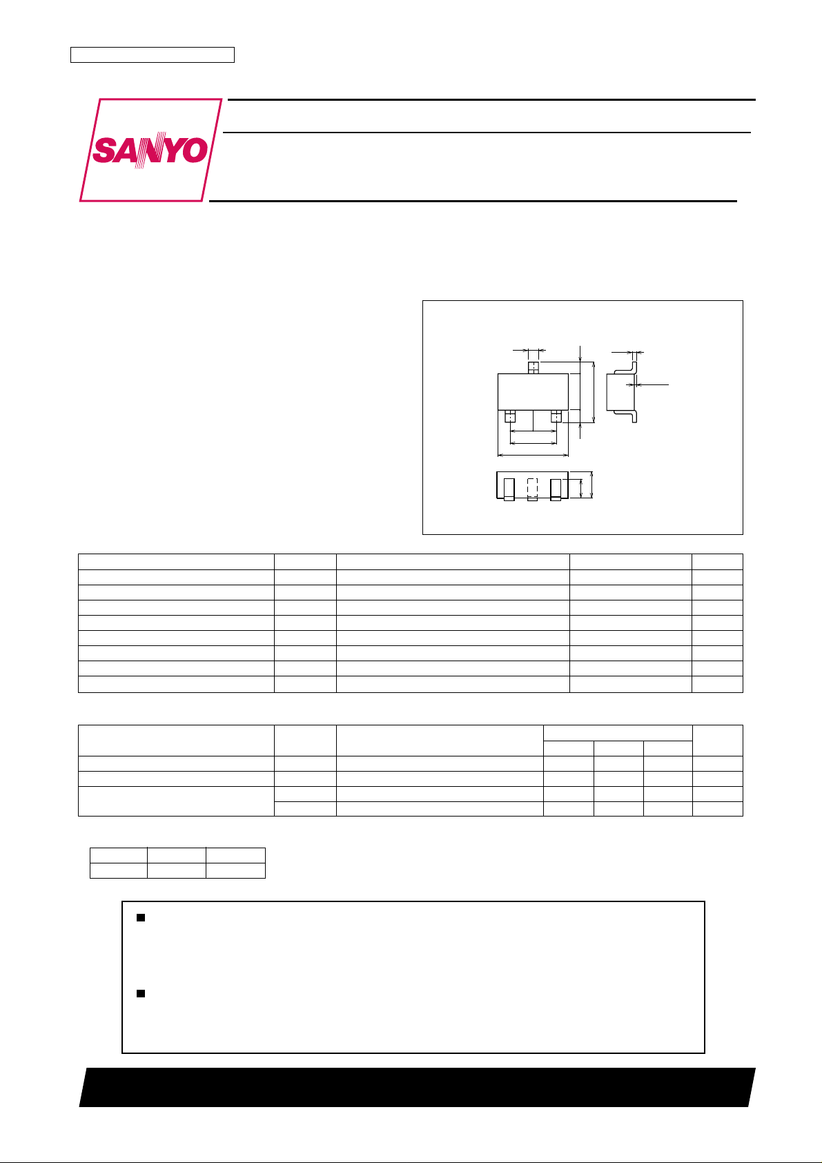
Package Dimensions
unit : mm
2018B
[2SC4412]
0.4
3
0.95
0.95
1
2
1.9
2.9
0.5
2.5
1.5
0.5
1.1
0.8
0.16
0 to 0.1
1 : Base
2 : Emitter
3 : Collector
SANYO : CP
Specifications
Absolute Maximum Ratings at T a=25°C
Parameter Symbol Conditions Ratings Unit
Collector-to-Base Voltage V
Collector-to-Emitter Voltage V
Emitter-to-Base Voltage V
Collector Current I
Collector Current (Pulse) I
Collector Dissipation P
Junction T emperature Tj 150 °C
Storage T emperature T stg --55 to +150 °C
CBO
CEO
EBO
C
CP
C
300 V
300 V
5V
50 mA
100 mA
250 mW
Electrical Characteristics at Ta=25°C
Parameter Symbol Conditions
Collector Cutoff Current I
Emitter Cutoff Current I
DC Current Gain
Marking : QT Continued on next page.
* : The 2SC4412 is classsified by 0.1mA hFE as follows.
Rank 4 5
h
FE 100 to 200 160 to 320
CBO
EBO
hFE1VCE=6V, IC=0.1mA 100* 320*
hFE2VCE=6V, IC=1mA 100
VCB=200V, IE=0 0.1 µA
VCE=4V, IC=0 0.1 µA
Any and all SANYO products described or contained herein do not have specifications that can handle
applications that require extremely high levels of reliability, such as life-support systems, aircraft's
control systems, or other applications whose failure can be reasonably expected to result in serious
physical and/or material damage. Consult with your SANYO representative nearest you before using
any SANYO products described or contained herein in such applications.
SANYO assumes no responsibility for equipment failures that result from using products at values that
exceed, even momentarily, rated values (such as maximum ratings, operating condition ranges, or other
parameters) listed in products specifications of any and all SANYO products described or contained
herein.
Ratings
min typ max
Unit
SANYO Electric Co.,Ltd. Semiconductor Company
TOKYO OFFICE Tokyo Bldg., 1-10, 1 Chome, Ueno, Taito-ku, TOKYO, 110-8534 JAPAN
11502 TS IM / D1598HA (KT) / 5189MO, TS
No.3019-1/3
Page 2
2SC4412
Continued from preceding page.
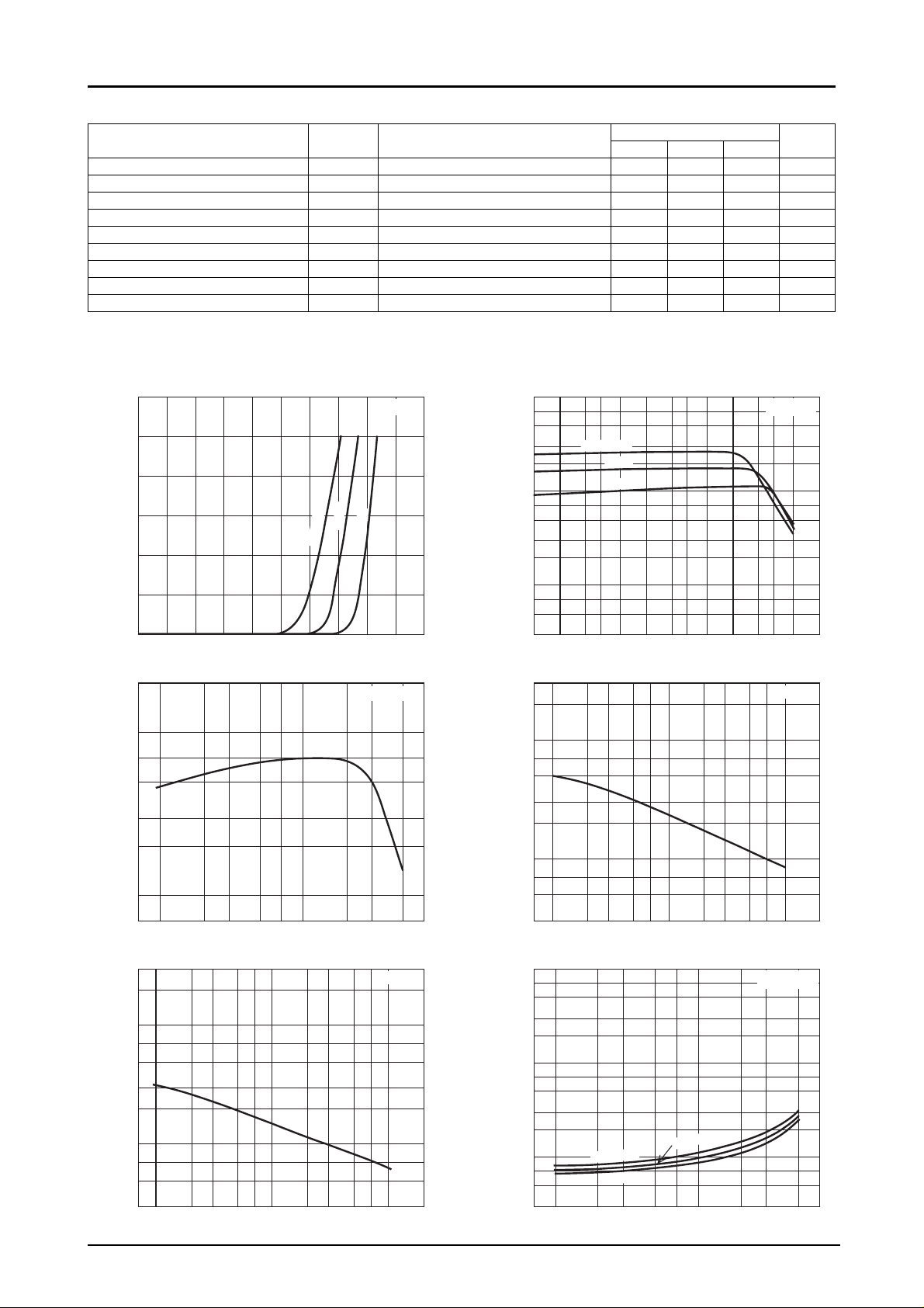
Parameter Symbol Conditions
Gain-Bandwidth Product f
Output Capacitance Cob VCB=30V , f=1MHz 1.5 pF
Reverse Transfer Capacitance Cre VCB=30V , f=1MHz 1.0 pF
DC Current Gain Ratio hFE ratio hFE1 / hFE2 0.95
Collector-to-Emitter Saturation Voltage
Base-to-Emitter Saturation Voltage VBE(sat) IC=10mA, IB=1mA 1.0 V
Collector-to-Base Breakdown Voltage V(
Collector-to-Emitter Breakdown Voltage V(
Emitter-to-Base Breakdown Voltage V(
I
-- V
C
-- mA
C
60
50
40
30
T
VCE(sat) IC=10mA, IB=1mA 1.0 V
BR)CBO
BR)CEO
BR)EBO
BE
Ta=75°C
20
Collector Current, I
10
0
0 0.2 0.4 0.6 0.8 1.0
Base-to-Emitter Voltage, VBE -- V
f
-- I
T
2
C
VCE=30V , IC=10mA 70 MHz
IC=10µA, IE=0 300 V
IC=1mA, RBE=∞ 300 V
IC=10µA, IC=0 5 V
VCE=6V
25°C
--25°C
ITR06793
VCE=30V
1000
7
5
3
2
FE
100
7
5
3
2
DC Current Gain, h
10
7
5
3
5235
0.1
Ta=75°C
25°C
--25°C
23 5
Collector Current, I
3
2
Ratings
min typ max
h
-- I
FE
1.0
Cob -- V
C
C
CB
10
-- mA
VCE=6V
23 5
ITR06794
f=1MHz
Unit
100
100
-- MHz
T
7
5
3
2
Gain-Bandwidth Product, f
10
7
72357
1.0
3
2
-- pF
10
7
5
3
2
1.0
7
5
Reverse Transfer Capacitance, Cre
3
1.0
23 57
Collector Current, IC -- mA
Cre -- V
10
ITR06795
CB
f=1MHz
23 51077235
Collector-to-Base Voltage, V
72
100
-- V
CB
ITR06797
10
-- pF
7
5
3
2
1.0
7
Output Capacitance, Cob
5
3
1.0
10
7
5
3
-- V
2
(sat)
CE
1.0
7
5
3
2
0.1
Collector-to-Emitter
Saturation V oltage, V
7
5
3
23 51077235
Collector-to-Base Voltage, V
V
(sat) -- I
CE
C
CB
-- V
100
ITR06796
27
IC / IB=10
25°C
Ta=75°C
--25°C
23 5772357
Collector Current, I
101.0
C
-- mA
ITR06798
No.3019-2/3
Page 3

10
7
5
-- V
(sat)
3
BE
2
1.0
7
Base-to-Emitter
Saturation V oltage, V
5
Ta= --25°C
75°C
2SC4412
V
(sat) -- I
BE
25°C
C
IC / IB=10
280
250
240
-- mW
200
C
160
120
80
Collector Dissipation, P
40
PC -- Ta
3
23 5772357
Collector Current, I
101.0
C
-- mA
ITR06799
0
0 20 40 60 80 100 120 140 160
Ambient Temperature, Ta -- °C
Specifications of any and all SANYO products described or contained herein stipulate the performance,
characteristics, and functions of the described products in the independent state, and are not guarantees
of the performance, characteristics, and functions of the described products as mounted in the customer's
products or equipment. To verify symptoms and states that cannot be evaluated in an independent device,
the customer should always evaluate and test devices mounted in the customer's products or equipment.
SANYO Electric Co., Ltd. strives to supply high-quality high-reliability products. However, any and all
semiconductor products fail with some probability. It is possible that these probabilistic failures could
give rise to accidents or events that could endanger human lives, that could give rise to smoke or fire,
or that could cause damage to other property. When designing equipment, adopt safety measures so
that these kinds of accidents or events cannot occur. Such measures include but are not limited to protective
circuits and error prevention circuits for safe design, redundant design, and structural design.
In the event that any or all SANYO products(including technical data,services) described or
contained herein are controlled under any of applicable local export control laws and regulations,
such products must not be exported without obtaining the export license from the authorities
concerned in accordance with the above law.
No part of this publication may be reproduced or transmitted in any form or by any means, electronic or
mechanical, including photocopying and recording, or any information storage or retrieval system,
or otherwise, without the prior written permission of SANYO Electric Co. , Ltd.
Any and all information described or contained herein are subject to change without notice due to
product/technology improvement, etc. When designing equipment, refer to the "Delivery Specification"
for the SANYO product that you intend to use.
Information (including circuit diagrams and circuit parameters) herein is for example only ; it is not
guaranteed for volume production. SANYO believes information herein is accurate and reliable, but
no guarantees are made or implied regarding its use or any infringements of intellectual property rights
or other rights of third parties.
ITR06800
This catalog provides information as of January, 2002. Specifications and information herein are subject
to change without notice.
No.3019-3/3
PS
 Loading...