

Page 1
Any and all SANYO products described or contained herein do not have specifications that can handle
applications that require extremely high levels of reliability, such as life-support systems, aircraft’s
control systems, or other applications whose failure can be reasonably expected to result in serious
physical and/or material damage. Consult with your SANYO representative nearest you before using
any SANYO products described or contained herein in such applications.
SANYO assumes no responsibility for equipment failures that result from using products at values that
exceed, even momentarily, rated values (such as maximum ratings, operating condition ranges,or other
parameters) listed in products specifications of any and all SANYO products described or contained
herein.
PNP/NPN Epitaxial Planar Silicon Transistors
High-Definition CRT Display
Video Output Applications
Ordering number:ENN2435B
2SA1536/2SC3951
SANYO Electric Co.,Ltd. Semiconductor Company
TOKYO OFFICE Tokyo Bldg., 1-10, 1 Chome, Ueno, Taito-ku, TOKYO, 110-8534 JAPAN
Applications
· High definition CRT display video output, wide-band
amplifier.
Features
· High fT : fT=600MHz.
· High breakdown voltage : V
· Small reverse transfer capacitance and excellent high
-frequency characteristic :
Cre=1.9pF/NPN, 2.4pF/PNP.
· Complementary PNP and NPN types.
· Adoption of FBET process.
· Micaless type.
( ) : 2SA1536
Specifications
Absolute Maximum Ratings at Ta = 25˚C
Electrical Characteristics at Ta = 25˚C
*hFE1 : The 2SA1536/2SC3951 are classified by 50mA hFE as follows : Continued on next page.
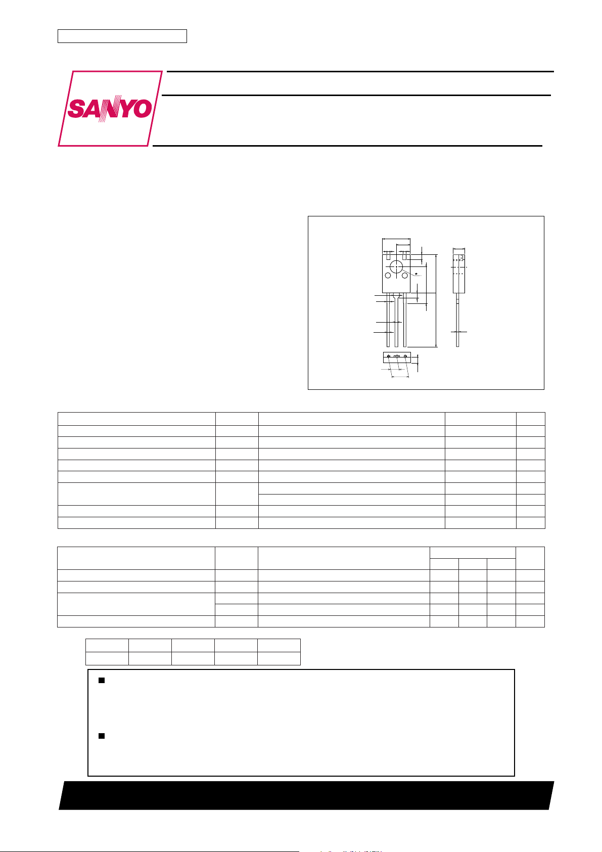
Package Dimensions
unit:mm
2042B
[2SA1536/2SC3951]
8.0
4.0
1.0
1.0
=70Vmin.
CEO
1.6
0.8
0.8
0.75
1
2.4
retemaraPlobmySsnoitidnoCsgnitaRtinU
egatloVesaB-ot-rotcelloCV
egatloVrettimE-ot-rotcelloCV
egatloVesaB-ot-rettimEV
tnerruCrotcelloCI
tnerruCrotcelloCkaePI
noitapissiDrotcelloCP
erutarepmeTnoitcnuJjT 051
erutarepmeTegarotSgtsT 051+ot55–
retemaraPlobmySsnoitidnoC
tnerruCffotuCrotcelloCI
tnerruCffotuCrettimEI
niaGtnerruCCD
tcudorPhtdiwdnaB-niaGf
knaRCDEF
h
EF
08ot04021ot06002ot001023ot061
OBC
OEC
OBE
C
PC
C
Tc=25˚C
V
OBC
OBE
hEF1V
hEF2V
T
BC
V
BE
EC
EC
V
EC
I,V06)–(=
0=1.0)–(Aµ
E
I,V2)–(=
0=0.1)–(Aµ
C
I,V01)–(=
C
I,V01)–(=
C
I,V01)–(=
C
Am05)–(=*04*023
Am002)–(=02
Am001)–(=006zHM
23
4.8
1.4
3.0
7.5
1.5
3.0
1.7
11.0
15.5
nimpytxam
3.3
0.7
1 : Emitter
2 : Collector
3 : Base
SANYO : TO-126ML
08)–(V
07)–(V
3)–(V
003)–(Am
006)–(Am
3.1W
8W
sgnitaR
˚C
˚C
tinU
53002RM (KT)/72098HA (KT)/9149MO/2247TA, TS No.2435-1/4
Page 2
Continued from preceding page.
retemaraPlobmySsnoitidnoC
ecnaticapaCtuptuOC
ecnaticapaCrefsnarTesreveRC
egatloVnoitarutaSrettimE-ot-rotcelloCV
egatloVnoitarutaSesaB-ot-rettimEV
I
-- V
C
--200
--160
CE
–mA
C
--120
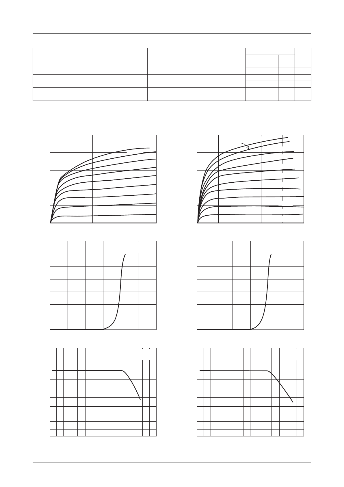
--8 0
Collector Current, I
--4 0
0
0 --4 --8 --16--1 2 --20
Collector-to-Emitter Voltage, VCE–V
I
-- V
--350
--300
C
BE
2SA1536/2SC3951
V
bo
er
--1.8mA
--1.6mA
--1.4mA
--1.2mA
--1.0mA
--0.8mA
--0.6mA
--0.4mA
--0.2mA
IB=0
2SA1536
VCE=--10V
V
I
)tas(EC
C
I
)tas(EB
C
2SA1536
ITR03875
BC
BC
I,Am05)–(=
B
I,Am05)–(=
B
sgnitaR
nimpytxam
zHM1=f,V03)–(=
zHM1=f,V03)–(=
Am5)–(=0.1)–(V
Am5)–(=0.1)–(V
I
-- V
200
160
C
2SC3951
1.8mA
CE
2.0mA
4.2Fp
)1.3(Fp
9.1Fp
)4.2(Fp
1.6mA
tinU
1.4mA
–mA
C
120
1.2mA
1.0mA
80
0.8mA
0.6mA
Collector Current, I
40
0.4mA
0.2mA
IB=0
ITR03876
2SC3951
VCE=10V
350
300
0
0
48 1612 20
Collector-to-Emitter Voltage, VCE–V
I
-- V
C
BE
–mA
C
Collector Current, I
--250
--200
--150
--100
--5 0
100
FE
DC Current Gain, h
0
0 --1.2--1 .0--0.8--0.6--0.4--0.2
3
2
7
5
3
2
10
7
5
Base-to-Emitter Voltage, VBE–V
--1 0
hFE -- I
23 557
C
72357
--100
Collector Current, IC–mA
ITR03877
2SA1536
VCE=--10V
ITR03879
--1000
–mA
C
Collector Current, I
FE
DC Current Gain, h
250
200
150
100
50
100
10
0
01.21.00.80.60.40.2
3
2
7
5
3
2
7
5
Base-to-Emitter Voltage, VBE–V
hFE -- I
23 557
10
C
72357
100
Collector Current, IC–mA
ITR03878
2SC3951
VCE=10V
1000
ITR03880
No.2435-2/4
Page 3

2
1000
– MHz
7
T
5
3
2
100
Gain-Bandwidth Product, f
7
5
57 3253257
--10
f
Collector Current, IC–mA
2
10
7
5
Cob -- V
T
-- I
C
CB
--100
2SA1536/2SC3951
2SA1536
VCE=--10V
1000
– MHz
T
100
Gain-Bandwidth Product, f
ITR03881
2SA1536
f=1MHz
10
f
-- I
T
2
7
5
3
2
7
5
3
357 3253257
2
7
5
10
Collector Current, IC–mA
Cob -- V
C
CB
2SC3951
VCE=10V
100
ITR03882
2SC3951
f=1MHz
(sat) – V
Output Capacitance, Cob – pF
Reverse Transfer Capacitance, Cre – pF
--1.0
CE
1.0
1.0
3
2
7
5
--1.0 --10
Collector-to-Base Voltage, VCB-- V
2
10
7
5
3
2
7
5
--1.0 --10
Collector-to-Base Voltage, VCB-- V
2
7
5
3
2
23 5757 2 3
Cre -- V
23 5757 23
VCE(sat) -- I
CB
C
2SA1536
IC / IB=10
57
ITR03883
2SA1536
f=1MHz
57
ITR03885
--100
--100
(sat) – V
Output Capacitance, Cob – pF
Reverse Transfer Capacitance, Cre – pF
CE
1.0
1.0
1.0
3
2
7
5
2
23 5757 2 3
1.0 10
Collector-to-Base Voltage, VCB-- V
Cre -- V
CB
57
ITR03884
2SC3951
100
f=1MHz
10
7
5
3
2
7
5
2
23 5757 23
1.0 10
Collector-to-Base Voltage, VCB-- V
VCE(sat) -- I
C
57
ITR03886
2SC3951
100
IC / IB=10
7
5
3
2
--0.1
7
Collector-to-Emitter
Saturation Voltage, V
5
3
57 2 3 57 2 3 57
--10
Collector Current, IC–mA
--100 --1000
ITR03887
0.1
7
Collector-to-Emitter
Saturation Voltage, V
5
3
57 2 3 57 2 3 57
10
Collector Current, IC–mA
100 1000
ITR03888
No.2435-3/4
Page 4

1000
–mA
C
2
ICP=600mA
7
5
IC=300mA
3
2
A S O
DC operation
Tc=25°C
2SA1536 / 2SC3951
10ms
1ms
2SA1536/2SC3951
10
8
–W
C
6
PC -- Ta
2SA1536 / 2SC3951
100
7
5
Collector Current, I
3
2
For PNP, minus sign is omitted.
10
537 2 537
Collector-to-Emitter Voltage, VCE–V
10 100
ITR03889
4
2
Collector Dissipation, P
1.3
0
No heat sink
100 140120 1602006040 80
Ambient Temperature, Ta – ˚C
ITR03890
Specifications of any and all SANYO products described or contained herein stipulate the performance,
characteristics, and functions of the described products in the independent state, and are not guarantees
of the performance, characteristics, and functions of the described products as mounted in the customer's
products or equipment. To verify symptoms and states that cannot be evaluated in an independent device,
the customer should always evaluate and test devices mounted in the customer's products or equipment.
SANYO Electric Co., Ltd. strives to supply high-quality high-reliability products. However, any and all
semiconductor products fail with some probability. It is possible that these probabilistic failures could
give rise to accidents or events that could endanger human lives, that could give rise to smoke or fire,
or that could cause damage to other property. When designing equipment, adopt safety measures so
that these kinds of accidents or events cannot occur. Such measures include but are not limited to protective
circuits and error prevention circuits for safe design, redundant design, and structural design.
In the event that any or all SANYO products(including technical data,services) described or
contained herein are controlled under any of applicable local export control laws and regulations,
such products must not be exported without obtaining the export license from the authorities
concerned in accordance with the above law.
No part of this publication may be reproduced or transmitted in any form or by any means, electronic or
mechanical, including photocopying and recording, or any information storage or retrieval system,
or otherwise, without the prior written permission of SANYO Electric Co. , Ltd.
Any and all information described or contained herein are subject to change without notice due to
product/technology improvement, etc. When designing equipment, refer to the "Delivery Specification"
for the SANYO product that you intend to use.
Information (including circuit diagrams and circuit parameters) herein is for example only ; it is not
guaranteed for volume production. SANYO believes information herein is accurate and reliable, but
no guarantees are made or implied regarding its use or any infringements of intellectual property rights
or other rights of third parties.
This catalog provides information as of May, 2002. Specifications and information herein are subject to
change without notice.
PS No.2435-4/4
 Loading...