

SANYO 2SC3920, 2SA1526 Datasheet
Ordering number:EN2150A
PNP/NPN Epitaxial Planar Silicon Transistors
2SA1526/2SC3920
Switching Applications (with Bias Resistance)
Applications
· Switching circuits, inverter circuits, interface circuits,
driver circuits.
Features
· On-chip bias resistance : R1=10kΩ, R2=10kΩ.
· Large current capacity : IC=500mA.
( ) : 2SA1526
Specifications
Absolute Maximum Ratings at Ta = 25˚C
retemaraPlobmySsnoitidnoCsgnitaRtinU
egatloVesaB-ot-rotcelloCV
egatloVrettimE-ot-rotcelloCV
egatloVesaB-ot-rettimEV
tnerruCrotcelloCI
)esluP(tnerruCrotcelloCI
noitapissiDrotcelloCP
erutarepmeTnoitcnuJjT 051
erutarepmeTegarotSgtsT 051+ot55–
OBC
OEC
OBE
C
PC
C
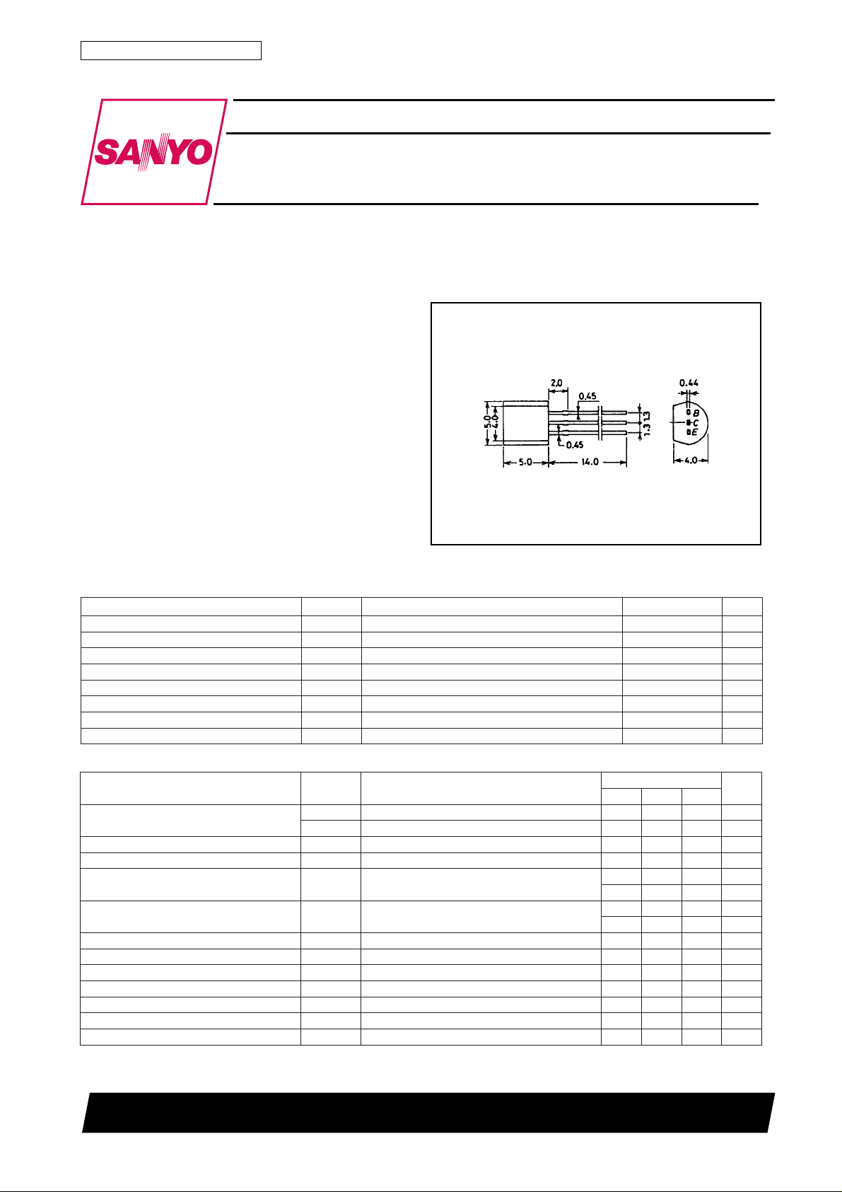
Package Dimensions
unit:mm
2003A
[2SA1526/2SC3920]
JEDEC : TO-92 B : Base
EIAJ : SC-43 C : Collector
SANYO : NP E : Emitter
05)–(V
05)–(V
01)–(V
005)–(Am
008)–(Am
006Wm
˚C
˚C
Electrical Characteristics at Ta = 25˚C
retemaraPlobmySsnoitidnoC
tnerruCffotuCrotcelloC
tnerruCffotuCrettimEI
niaGtnerruCCDh
tcudorPhtdiwdnaB-niaGf
ecnaticapaCtuptuOC
egatloVnoitarutaSrettimE-ot-rotcelloCV
egatloVnwodkaerBesaB-ot-rotcelloCV
egatloVnwodkaerBrettimE-ot-rotcelloCV
egatloVetatS-FFOtupnIV
egatloVetatS-NOtupnI
ecnatsiseRtupnI1R70131kΩ
oitaRecnatsiseR2R/1R9.00.11.1
I
I
V
V
OBC
OEC
OBE
EF
T
bo
BC
V
EC
V
BE
V
EC
V
EC
V
BC
I
)tas(EC
C
I
OBC)RB(
C
I
OEC)RB(
C
V
)ffo(I
EC
V
)no(I
EC
I,V04)–(=
0=1.0)–(Aµ
E
I,V04)–(=
0=5.0)–(Aµ
B
I,V5)–(=
0=591)–(052)–(063)–(Aµ
C
I,V5)–(=
C
I,Am02)–(=
I,Aµ01)–(=
E
I,V5)–(=
C
Am01)–(=05
I,V01)–(=
Am5)–(=
C
zHM1=f,V01)–(=
Am1)–(=1.0)–(3.0)–(V
B
0=05)–(V
R,Aµ001)–(=
=∞ 05)–(V
EB
Aµ001)–(=8.0)–(1.1)–(5.1)–(V
I,V2.0)–(=
C
Am01)–(=0.1)–(0.2)–(0.4)–(V
nimpytxam
SANYO Electric Co.,Ltd. Semiconductor Bussiness Headquaters
TOKYO OFFICE Tokyo Bldg., 1-10, 1 Chome, Ueno, Taito-ku, TOKYO, 110-8534 JAPAN
71598HA (KT)/3317KI/D086TA, TS No.2150-1/2
sgnitaR
052zHM
)002(zHM
7.3Fp
)5.5(Fp
tinU
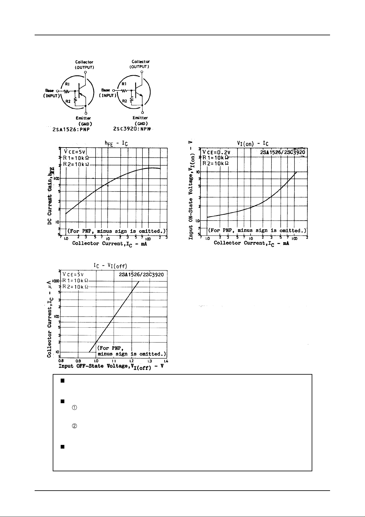
Electrical Connection
2SA1526/2SC3920
No products described or contained herein are intended for use in surgical implants, life-support systems,
aerospace equipment, nuclear power control systems, vehicles, disaster/crime-prevention equipment and
the like, the failure of which may directly or indirectly cause injury, death or property loss.
Anyone purchasing any products described or contained herein for an above-mentioned use shall:
Accept full responsibility and indemnify and defend SANYO ELECTRIC CO., LTD., its affiliates,
subsidiaries and distributors and all their officers and employees, jointly and severally, against any
and all claims and litigation and all damages, cost and expenses associated with such use:
Not impose any responsibilty for any fault or negligence which may be cited in any such claim or
litigation on SANYO ELECTRIC CO., LTD., its affiliates, subsidiaries and distributors or any of
their officers and employees jointly or severally.
Information (including circuit diagrams and circuit parameters) herein is for example only; it is not guaranteed for volume production. SANYO believes information herein is accurate and reliable, but no guarantees
are made or implied regarding its use or any infringements of intellectual property rights or other rights of
third parties.
This catalog provides information as of July, 1998. Specifications and information herein are subject to
change without notice.
PS No.2150-2/2
 Loading...