

SANYO 2SC3661 Datasheet
SANYO Electric Co.,Ltd. Semiconductor Bussiness Headquaters
TOKYO OFFICE Tokyo Bldg., 1-10, 1 Chome, Ueno, Taito-ku, TOKYO, 110-8534 JAPAN
Any and all SANYO products described or contained herein do not have specifications that can handle
applications that require extremely high levels of reliability, such as life-support systems, aircraft’s
control systems, or other applications whose failure can be reasonably expected to result in serious
physical and/or material damage. Consult with your SANYO representative nearest you before using
any SANYO products described or contained herein in such applications.
SANYO assumes no responsibility for equipment failures that result from using products at values that
exceed, even momentarily, rated values (such as maximum ratings, operating condition ranges,or other
parameters) listed in products specifications of any and all SANYO products described or contained
herein.
NPN Epitaxial Planar Silicon Transistor
High hFE, Low-Frequency
General-Purpose Amplifier Applications
Ordering number:EN1854A
2SC3661
Applications
· Low frequency general-purpose amplifiers, drivers,
muting circuit.
Features
· Very small-sized package permitting 2SC3661-used
sets to be made smaller, slimmer.
· Adoption of FBET process.
· High DC current gain (hFE=800 to 3200).
· Low collector-to-emitter saturation voltage
(V
· High V
Specifications
Absolute Maximum Ratings at Ta = 25˚C
≤0.5V).
CE(sat)
(V
EBO
tnerruCrotcelloCI
≥15V).
EBO
retemaraPlobmySsnoitidnoCsgnitaRtinU
egatloVesaB-ot-rotcelloCV
egatloVrettimE-ot-rotcelloCV
egatloVesaB-ot-rettimEV
)esluP(tnerruCrotcelloCI
noitapissiDrotcelloCP
erutarepmeTnoitcnuJjT 521
erutarepmeTegarotSgtsT 521+ot55–
OBC
OEC
OBE
C
PC
C
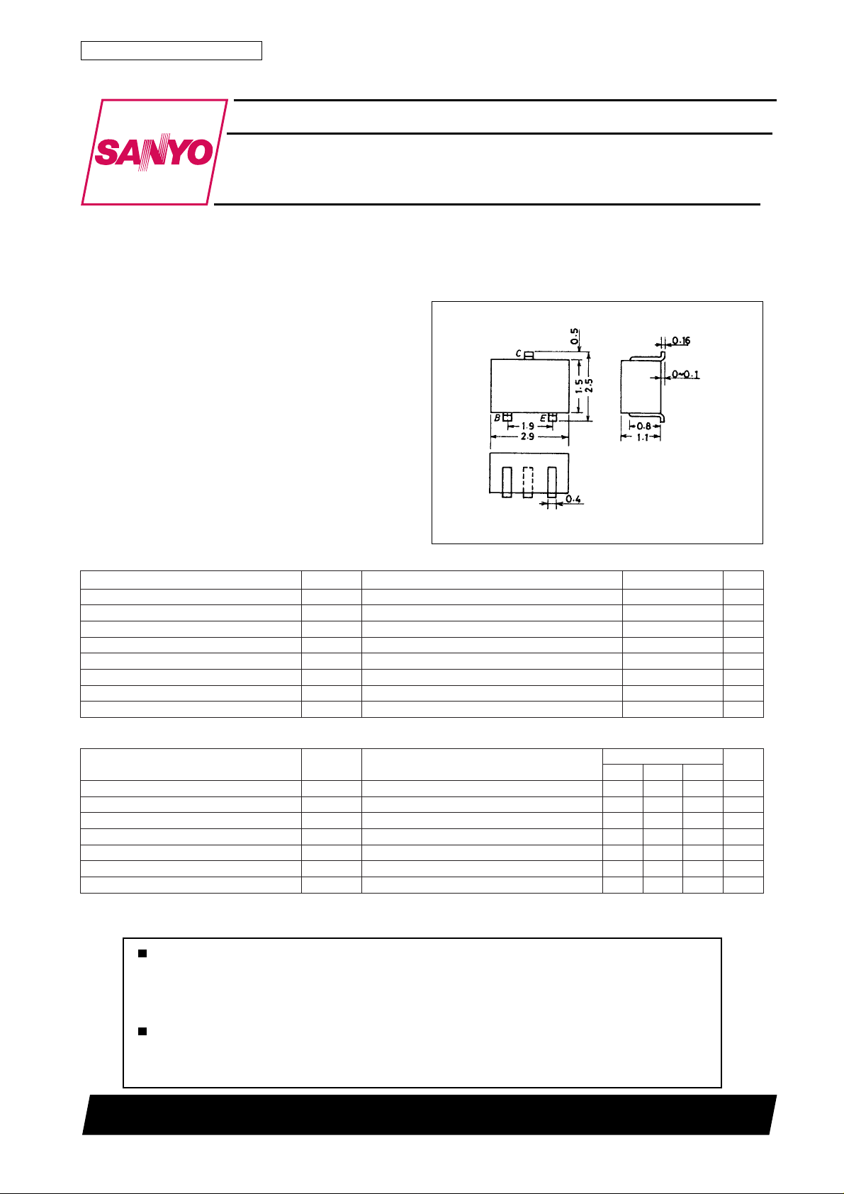
Package Dimensions
unit:mm
2018A
[2SC3661]
C : Collector
B : Base
E : Emitter
SANYO : CP
03V
52V
51V
003Am
005Am
002Wm
˚C
˚C
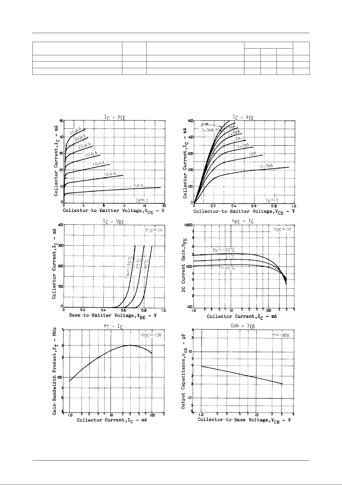
Electrical Characteristics at Ta = 25˚C
retemaraPlobmySsnoitidnoC
Marking : FY
tnerruCffotuCrotcelloCI
tnerruCffotuCrettimEI
niaGtnerruCCD
tcudorPhtdiwdnaB-niaGf
ecnaticapaCtuptuOC
egatloVnoitarutaSrettimE-ot-rotcelloCV
egatloVnoitarutaSrettimE-ot-esaBV
h
V
OBC
V
OBE
V
EF
V
T
V
bo
I
)tas(EC
C
I
C
)tas(EB
I,V02=
BC
BE
EC
EC
BC
0=1.0Aµ
E
I,V01=
0=1.0Aµ
C
I,V5=
Am01=
C
I,V01=
Am01=
C
zHM1=f,V01=
I,Am002=
Am4=
B
I,Am002=
Am4=
B
N2098HA (KT)/4237AT/N195KI, TS No.1854–1/3
nimpytxam
00800510023
sgnitaR
052zHM
7.2Fp
21.05.0V
58.02.1V
tinU
2SC3661
retemaraPlobmySsnoitidnoC
egatloVnwodkaerBesaB-ot-rotcelloCV
egatloVnwodkaerBrettimE-ot-rotcelloCV
egatloVnwodkaerBesaB-ot-rettimEV
I
OBC)RB(
I
OEC)RB(
I
OBE)RB(
I,Aµ01=
C
C
E
0=03V
E
I,Am1=
=0 52V
B
I,Aµ01=
0=51V
C
sgnitaR
nimpytxam
tinU
No.1854–2/3
 Loading...