

SANYO 2SC3649, 2SA1419 Datasheet
Ordering number:EN2007A
PNP/NPN Epitaxial Planar Silicon Transistors
2SA1419/2SC3649
High-Voltage Switching Applications
Features
· Adoption of FBET, MBIT processes.
· High breakdown voltage and large current capacity.
· Very small size making it easy to provide high-
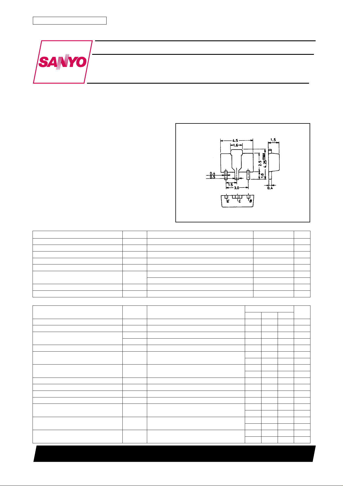
Package Dimensions
unit:mm
2038
density hybrid ICs.
( ) : 2SA1419
Specifications
Absolute Maximum Ratings at Ta = 25˚C
retemaraPlobmySsnoitidnoCsgnitaRtinU
egatloVesaB-ot-rotcelloCV
egatloVrettimE-ot-rotcelloCV
egatloVesaB-ot-rettimEV
tnerruCrotcelloCI
)esluP(tnerruCrotcelloCI
noitapissiDrotcelloCP
erutarepmeTnoitcnuJjT 051
erutarepmeTegarotSgtsT 051+ot55–
Electrical Characteristics at Ta = 25˚C
retemaraPlobmySsnoitidnoC
tnerruCffotuCrotcelloCI
tnerruCffotuCrettimEI
niaGtnerruCCD
tcudorPhtdiwdnaB-niaGf
ecnaticapaCtuptuOC
egatloVnoitarutaSrettimE-ot-rotcelloCV
egatloVnoitarutaSrettimE-ot-esaBV
egatloVnwodkaerBesaB-ot-rotcelloCV
egatloVnwodkaerBrettimE-ot-rotcelloCV
egatoVnwodkaerBesaB-ot-rettimEV
emiTNO-nruTt
emiTegatotSt
emiTllaFt
OBC
OEC
OBE
C
PC
C
Moutned on ceramic board (250mm2×0.8mm)
V
OBC
OBE
hEF1VECI,V5)–(=
hEF2VECI,V5)–(=
T
bo
no
gts
f
BC
V
BE
V
EC
V
BC
I
)tas(EC
C
I
)tas(EB
C
I
OBC)RB(
C
I
OEC)RB(
C
I
OBE)RB(
E
I,V021)–(=
0=1)–(Aµ
E
I,V4)–(=
0=1)–(Aµ
C
C
C
I,V01)–(=
C
I,Am005)–(=
I,Am005)–(=
I,Aµ01)–(=
E
R,Am1)–(=
I,Aµ01)–(=
C
Am001)–(=*001*004
Am01)–(=08
Am05)–(=021zHM
zHM1=f,V01)–(=
B
B
EB
Am05)–(=
Am05)–(=58.0)–(2.1)–(V
0=081)–(V
=∞ 061)–(V
0=6)–(V
[2SA1419/2SC3649]
E : Emitter
C : Collector
B : Base
SANYO : PCP
(Bottom view)
081)–(V
061)–(V
6)–(V
5.1)–(A
5.2)–(A
005Wm
5.1W
˚C
˚C
sgnitaR
nimpytxam
)22(Fp
41Fp
)002–()005–(Vm
031054Vm
.tiucriCtseTdeificepseeS
.tiucriCtseTdeificepseeS
.tiucriCtseTdeificepseeS
)04(sn
04sn
)7.0(sµ
2.1sµ
)04(sn
08sn
tinU
SANYO Electric Co.,Ltd. Semiconductor Bussiness Headquaters
TOKYO OFFICE Tokyo Bldg., 1-10, 1 Chome, Ueno, Taito-ku, TOKYO, 110-8534 JAPAN
71598HA (KT)/4277TA, TS No.2007-1/4
2SA1419/2SC3649
* : The 2SA1419/2SC3649 are classified by 100mA hFE as follows :
002R001082S041004T002
Marking 2SA1419 : AE hFE rank : R, S, T
2SC3649 : CE
Switching Time T est Circuit
(For PNP, the polarity is reversed)
Unit (resistance : Ω, capacitance : F)
No.2007-2/4
 Loading...