

Page 1
Any and all SANYO products described or contained herein do not have specifications that can handle
applications that require extremely high levels of reliability, such as life-support systems, aircraft’s
control systems, or other applications whose failure can be reasonably expected to result in serious
physical and/or material damage. Consult with your SANYO representative nearest you before using
any SANYO products described or contained herein in such applications.
SANYO assumes no responsibility for equipment failures that result from using products at values that
exceed, even momentarily, rated values (such as maximum ratings, operating condition ranges,or other
parameters) listed in products specifications of any and all SANYO products described or contained
herein.
PNP/NPN Epitaxial Planar Silicon Transistors
High V
EBO
, AF Amp Applications
Ordering number:ENN1048C
2SA1252/2SC3134
SANYO Electric Co.,Ltd. Semiconductor Company
TOKYO OFFICE Tokyo Bldg., 1-10, 1 Chome, Ueno, Taito-ku, TOKYO, 110-8534 JAPAN
Features
· High V
· Wide ASO and high durability against breakdown.
( ) : 2SA1252
Specifications
Absolute Maximum Ratings at Ta = 25˚C
.
EBO
retemaraPlobmySsnoitidnoCsgnitaRtinU
egatloVesaB-ot-rotcelloCV
egatloVrettimE-ot-rotcelloCV
egatloVesaB-ot-rettimEV
tnerruCrotcelloCI
)esluP(tnerruCrotcelloCI
noitapissiDrotcelloCP
erutarepmeTnoitcnuJjT 521
erutarepmeTegarotSgtsT 521+ot55–
OBC
OEC
OBE
C
PC
C
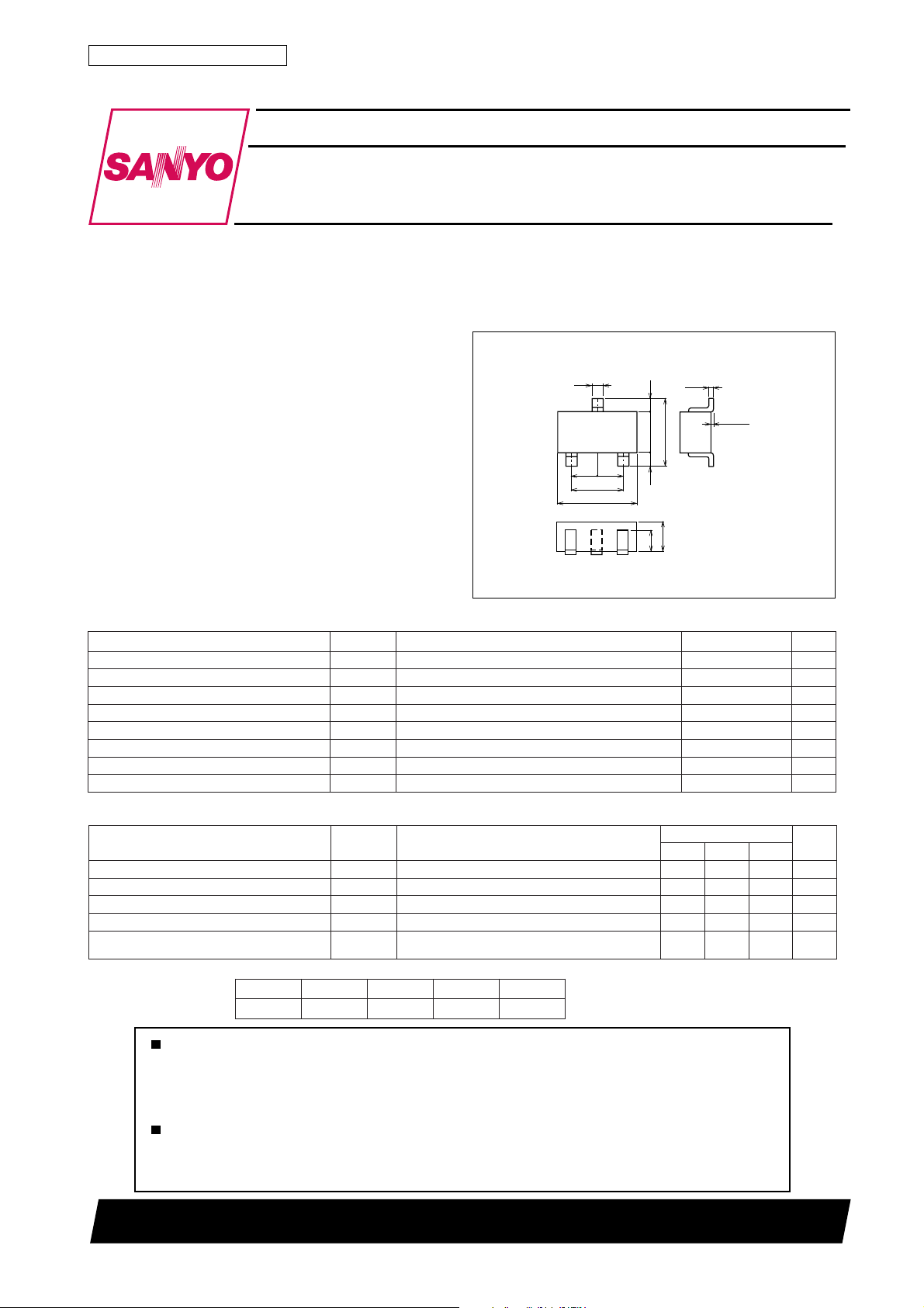
Package Dimensions
unit:mm
2018B
1
[2SA1252/2SC3134]
0.4
0.95
3
0.95
1.9
2.9
0.5
1.5
2
0.5
0.8
0.16
2.5
1.1
0 to 0.1
1 : Base
2 : Emitter
3 : Collector
SANYO : CP
06)–(V
05)–(V
51)–(V
051)–(Am
003)–(Am
002Wm
˚C
˚C
Electrical Characteristics at Ta = 25˚C
retemaraPlobmySsnoitidnoC
tnerruCffotuCrotcelloCI
tnerruCffotuCrettimEI
niaGtnerruCCDh
tcudorPhtdiwdnaB-niaGf
ecnaticapaCtuptuOboCV
V
OBC
OBE
EF
T
BC
V
BE
V
EC
V
EC
BC
I,V04)–(=
0=1.0)–(Aµ
E
I,V01)–(=
0=1.0)–(Aµ
C
I,V6)–(=
Am1)–(=*09*065
C
I,V6)–(=
Am1)–(=001zHM
C
zHM1=f,V6)–(=
nimpytxam
* : The 2SA1252/2SC3134 are classified as follows according to hFE at 1mA : Continued on next page.
Marking 2SA1252 : D
2SC3134 : H
hFE rank : 4, 5, 6, 7
knaR 4567
h
EF
081ot09072ot531004ot002006ot003
70502TN (KT)/71598HA (KT)/3187AT/3155MW, TS No.1048-1/4
sgnitaR
)5.3(
2.2
tinU
Fp
Page 2
Continued from preceding page.
retemaraPlobmySsnoitidnoC
2SA1252/2SC3134
egatloVnoitarutaSrettimE-ot-rotcelloCV
egatloVnwodkaerBesaB-ot-rotcelloCV
egatloVnwodkaerBrettimE-ot-rotcelloCV
egatloVnwodkaerBesaB-ot-rettimEV
I
)tas(EC
C
I
OBC)RB(
C
I
OEC)RB(
C
I
OBE)RB(
E
I,Am05)–(=
Am5)–(=5.0)–(V
B
I,Aµ01)–(=
0=06)–(V
E
R,Am1)–(=
=∞ 05)–(V
EB
I,Aµ01)–(=
0=51)–(V
C
sgnitaR
nimpytxam
tinU
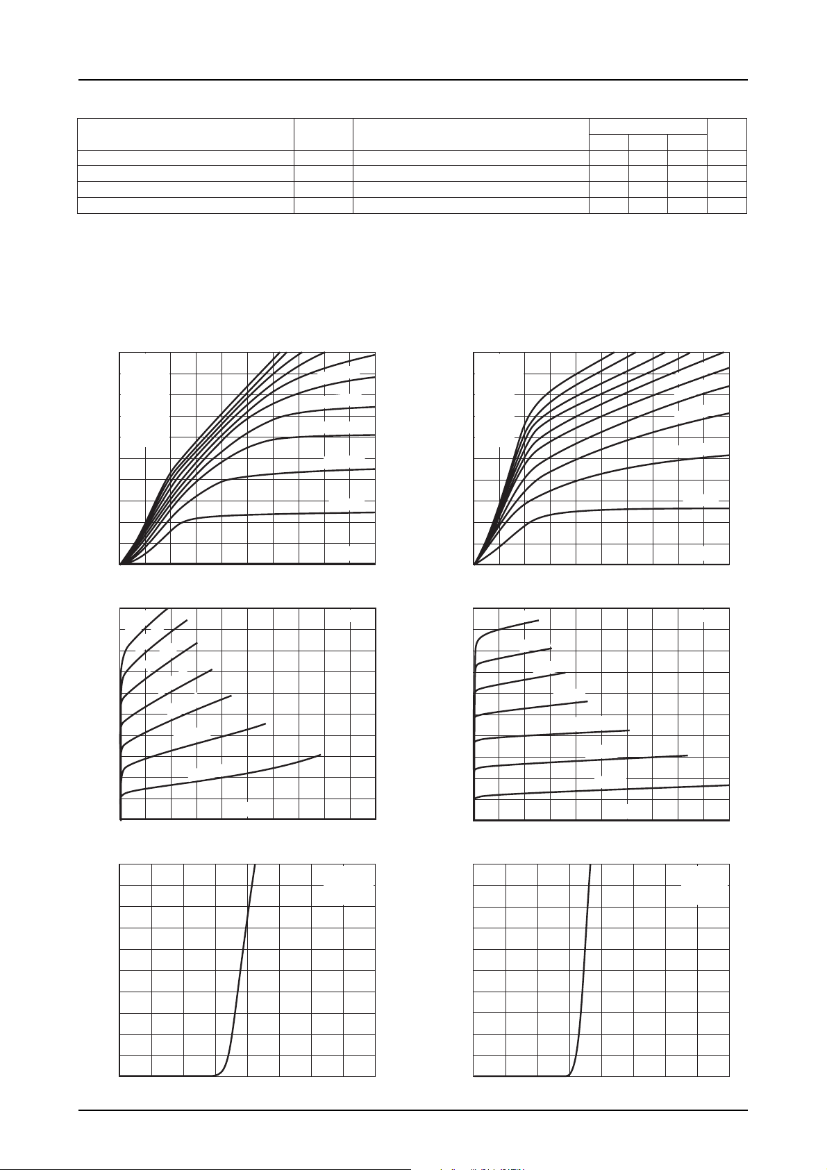
–mA
C
Collector Current, I
–mA
C
Collector Current, I
--
50
--
40
--
30
--
20
--
10
--
20
--
16
--
12
--
--
2SA1252
From top
--500µA
--450µA
--400µA
--350µA
--300µA
0
0
--70µA
8
4
IC -- V
--
0.2
--
0.4
CE
--
0.6
Collector-to-Emitter Voltage, VCE–V
IC -- V
CE
--60µA
--50µA
--40µA
--30µA
--20µA
--10µA
--250
--200
--150µA
--100µA
--50µA
--
0.8
2SA1252
µA
µA
=0
I
B
ITR03076
–mA
C
50
40
30
IC -- V
2SC3134
From top
500µA
450µA
400µA
350µA
300µA
CE
250
200µA
150µA
µA
100µA
20
50µA
Collector Current, I
10
=0
I
--
1.0
0
0 0.2 0.4 0.6 0.8 1.0
Collector-to-Emitter Voltage, VCE–V
–mA
C
20
16
70
µA
60µA
IC -- V
50µA
12
8
40µA
CE
30µA
B
ITR03077
2SC3134
20µA
Collector Current, I
4
10µA
--
–mA
C
Collector Current, I
--
--
--
--
100
=0
I
0
0
--
10
Collector-to-Emitter Voltage, VCE–V
B
--
20
IC -- V
--
BE
30
--
40
ITR03078
--
50
2SA1252
0
01020304050
Collector-to-Emitter Voltage, VCE–V
100
IC -- V
VCE=--6V
80
Pulse
80
I
B
BE
=0
ITR03079
2SC3134
VCE=6V
Pulse
–mA
C
60
40
20
0
0
--
0.4
--
0.8
--
1.2
Base-to-Emitter Voltage, VBE–V
ITR03080
--
1.6
60
40
Collector Current, I
20
0
0 0.4 0.8 1.2 1.6
Base-to-Emitter Voltage, VBE–V
ITR03081
No.1048-2/4
Page 3

1000
FE
2SA1252/2SC3134
hFE -- I
7
5
3
2
C
2SA1252
VCE=--6V
Pulse
1000
FE
7
5
3
2
hFE -- I
C
2SC3134
VCE=6V
Pulse
100
DC Current Gain, h
1000
– MHz
T
100
Gain-Bandwidth Product, f
10
7
5
3
2
25 25 2 25
--
0.1
--
1.0
Collector Current, IC–mA
fT -- I
7
5
3
2
7
5
3
2
7
3
2
--
1.0
23 357
Collector Current, IC–mA
--
10
Cob -- V
DC Current Gain, h
--
10
--
100
ITR03082
C
2SA1252
VCE=--6V
Pulse
– MHz
Gain-Bandwidth Product, f
22
57
--
100
ITR03084
CB
2SA1252
f=1MHz
100
7
5
3
2
25 25 2 25
0.1 1.0 10 100
1000
7
5
3
T
2
100
7
5
3
2
10
7
0.1
3
2
Collector Current, IC–mA
fT -- I
C
23 357
Collector Current, IC–mA
Cob -- V
22
10
CB
57
ITR03083
2SC3134
VCE=6V
Pulse
100
ITR03085
2SC3134
f=1MHz
10
7
5
3
2
Output Capacitance, Cob – pF
1.0
7
--
1.0
Collector-to-Base Voltage, VCB-- V
3
2
--
1.0
7
(sat) – V
5
CE
3
2
--
0.1
7
Collector-to-Emitter
Saturation Voltage, V
5
3
23357
--
1.0
23 3557
VCE(sat) -- I
2
--
10
C
57
ITR03086
2SA1252
IC / IB=10
57
Collector Current, IC–mA
2
--
10
--
100
ITR03088
10
7
5
3
2
Output Capacitance, Cob – pF
1.0
(sat) – V
Saturation Voltage, V
CE
1.0
0.1
7
3
2
7
5
3
2
7
5
3
1.0
--
100
Collector-to-Emitter
2
23 3557
1.0
Collector-to-Base Voltage, VCB-- V
VCE(sat) -- I
2
10
C
57
ITR03087
100
2SC3134
IC / IB=10
23357
57
Collector Current, IC–mA
2
10
100
ITR03089
2
No.1048-3/4
Page 4

P
-- Ta
240
200
–mW
160
C
120
80
40
Collector Dissipation, P
0
0 20 40 60 80 100 120 140
Ambient Temperature, Ta – ˚C
C
2SA1252 / 2SC3134
2SA1252/2SC3134
ITR03090
Specifications of any and all SANYO products described or contained herein stipulate the performance,
characteristics, and functions of the described products in the independent state, and are not guarantees
of the performance, characteristics, and functions of the described products as mounted in the customer's
products or equipment. To verify symptoms and states that cannot be evaluated in an independent device,
the customer should always evaluate and test devices mounted in the customer's products or equipment.
SANYO Electric Co., Ltd. strives to supply high-quality high-reliability products. However, any and all
semiconductor products fail with some probability. It is possible that these probabilistic failures could
give rise to accidents or events that could endanger human lives, that could give rise to smoke or fire,
or that could cause damage to other property. When designing equipment, adopt safety measures so
that these kinds of accidents or events cannot occur. Such measures include but are not limited to protective
circuits and error prevention circuits for safe design, redundant design, and structural design.
In the event that any or all SANYO products(including technical data,services) described or
contained herein are controlled under any of applicable local export control laws and regulations,
such products must not be exported without obtaining the export license from the authorities
concerned in accordance with the above law.
No part of this publication may be reproduced or transmitted in any form or by any means, electronic or
mechanical, including photocopying and recording, or any information storage or retrieval system,
or otherwise, without the prior written permission of SANYO Electric Co. , Ltd.
Any and all information described or contained herein are subject to change without notice due to
product/technology improvement, etc. When designing equipment, refer to the "Delivery Specification"
for the SANYO product that you intend to use.
Information (including circuit diagrams and circuit parameters) herein is for example only ; it is not
guaranteed for volume production. SANYO believes information herein is accurate and reliable, but
no guarantees are made or implied regarding its use or any infringements of intellectual property rights
or other rights of third parties.
This catalog provides information as of July, 2002. Specifications and information herein are subject to
change without notice.
PS No.1048-4/4
 Loading...