

Page 1
Any and all SANYO products described or contained herein do not have specifications that can handle
applications that require extremely high levels of reliability, such as life-support systems, aircraft’s
control systems, or other applications whose failure can be reasonably expected to result in serious
physical and/or material damage. Consult with your SANYO representative nearest you before using
any SANYO products described or contained herein in such applications.
SANYO assumes no responsibility for equipment failures that result from using products at values that
exceed, even momentarily, rated values (such as maximum ratings, operating condition ranges,or other
parameters) listed in products specifications of any and all SANYO products described or contained
herein.
PNP/NPN Epitaxial Planar Silicon Transistors
High-Voltage Low-Noise Amp Applications
Ordering number:ENN572E
2SA1016, 1016K/2SC2362, 2362K
SANYO Electric Co.,Ltd. Semiconductor Company
TOKYO OFFICE Tokyo Bldg., 1-10, 1 Chome, Ueno, Taito-ku, TOKYO, 110-8534 JAPAN
5.0
4.0
0.5
0.6
2.0
14.0
5.0
0.45
0.45
4.0
0.44
1.3
1.3
123
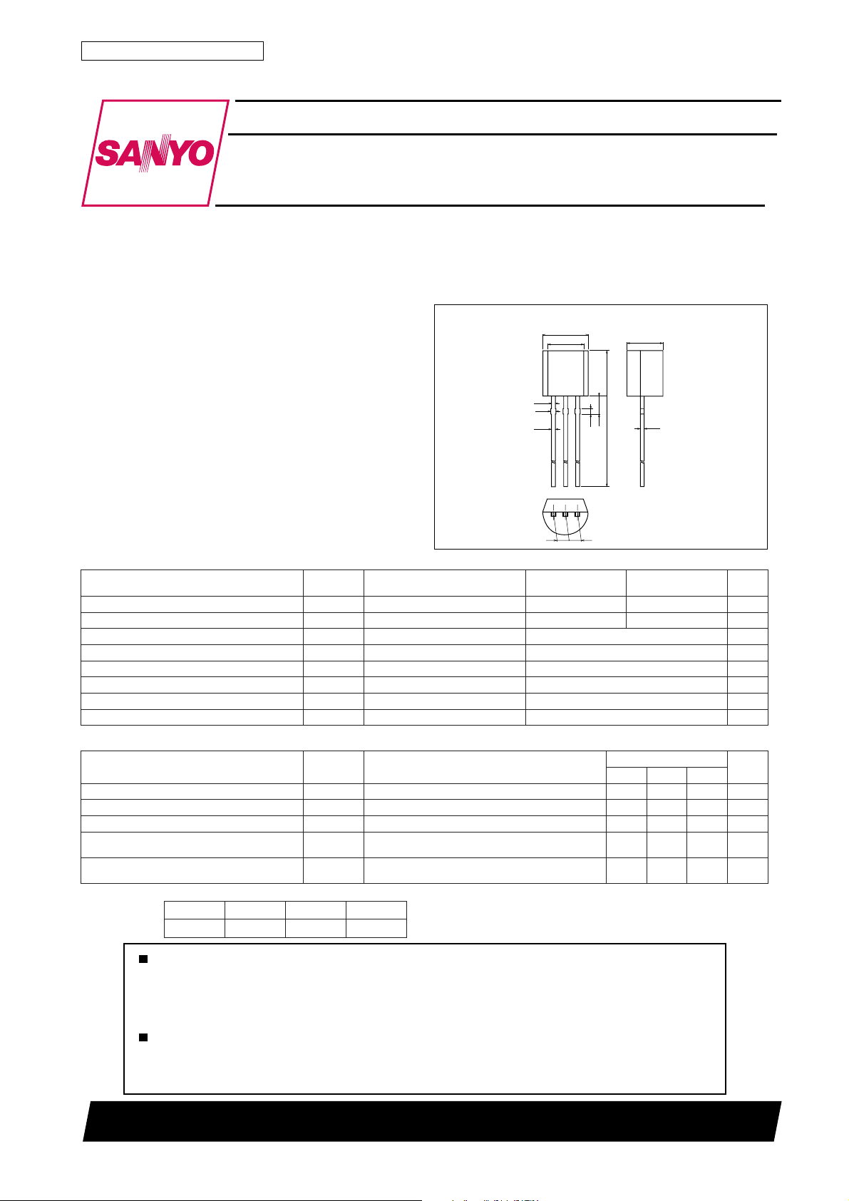
Package Dimensions
unit:mm
2003B
[2SA1016, 1016K/2SC2362, 2362K]
1 : Emitter
( ) : 2SA1016, 1016K
Specifications
Absolute Maximum Ratings at Ta = 25˚C
retemaraPlobmySsnoitidnoC2632CS2,6101AS2
egatloVesaB-ot-rotcelloCV
egatloVrettimE-ot-rotcelloCV
egatloVesaB-ot-rettimEV
tnerruCrotcelloCI
)esluP(tnerruCrotcelloCI
noitapissiDrotcelloCP
erutarepmeTnoitcnuJjT 521
erutarepmeTegarotSgtsT 521+ot55–
OBC
OEC
OBE
C
PC
C
Electrical Characteristics at Ta = 25˚C
retemaraPlobmySsnoitidnoC
tnerruCffotuCrotcelloCI
tnerruCffotuCrettimEI
niaGtnerruCCDh
tcudorPhtdiwdnaB-niaGf
ecnaticapaCtuptuOC
* : The 2SA1016, K/2SC2362, K are classified by 1mA hFE as follows : Continued on next page.
knaRFGH
h
EF
023ot061065ot082069ot084
V
OBC
OBE
EF
T
bo
BC
V
BE
V
EC
V
EC
V
BC
I,V08)–(=
0=0.1)–(Aµ
E
I,V4)–(=
0=0.1)–(Aµ
C
I,V6)–(=
Am1)–(=*061*069
C
I,V6)–(=
Am1)–(=
C
zHM1=f,V01)–(=
021)–(051)–(V
001)–(021)–(V
nimpytxam
2 : Collecor
3 : Base
SANYO : NP
,K6101AS2
K2632CS2
sgnitaR
)011(
031
)2.2(
8.1
tinU
5)–(V
05)–(Am
001)–(Am
004Wm
˚C
˚C
tinU
zHM
Fp
70502TN (KT)/71598HA (KT)/3187AT/3075KI/1313KI No.572-1/4
Page 2

Continued from preceding page.
retemaraPlobmySsnoitidnoC
leveLesioNV
leveLkaePesioNV
2SA1016, 1016K/2SC2362, 2362K
egatloVnoitarutaSrettimE-ot-rotcelloCV
egatloVnwodkaerBesaB-ot-rotcelloC(V
egatloVnwodkaerBrettimE-ot-rotcelloCV
egatloVnwodkaerBesaB-ot-rettimEV
I
)tas(EC
C
I
C
OBC)RB
I
C
I
C
OEC)RB(
I
C
I
OBE)RB(
E
V
)eva(ON
CC
V
)kaep(ON
CC
I,Am01)–(=
Am1)–(=5.0)–(V
B
I,Aµ01)–(=
E
I,Aµ01)–(=
E
R,Am1)–(=
=∞ ]2632C,6101A[001)–(V
EB
R,Am1)–(=
=∞ ]K2632C,K6101A[021)–(V
EB
I,Aµ01)–(=
0=5)–(V
C
I,V03=
R,Am1=
C
I,V03=
C
k65= Ω V,
g
R,Am1=
g
k65= Ω,
G
GV
sgnitaR
nimpytxam
]2632C,6101A[0=021)–(V
]K2632C,K6101A[0=051)–(V
zHk1/Bd77=53Vm
zHk1/Bd77=002Vm
tinU
A
--300
IC -- V
A
µ
--250
--12
--10
–mA
--8
C
--6
--4
Collector Current, I
--2
0
0 --10 --20 --30 --40
--350
µ
A
µ
--200
CE
A
µ
--150
--100
Collector-to-Emitter Voltage, VCE–V
IB -- V
--100
2SA1016, 1016K
VCE=
--80
– µA
--60
B
--40
--5V
BE
2SA1016, 1016K
A
µ
A
µ
A
µ
--50
IB=0
ITR02951
--50
12
10
–mA
8
C
6
4
Collector Current, I
2
0
01020304050
IC -- V
Collector-to-Emitter Voltage, VCE–V
100
2SC2362, 2362K
IB -- V
CE
250
BE
200
µ
150
A
µ
100
2SC2362, 2362K
A
A
µ
A
µ
A
µ
50
IB=0
ITR02952
VCE=5V
80
– µA
60
B
40
Base Current, I
--20
0
0 --0.2 --0.4 --0.6 --0.8 --1.0
Base-to-Emitter Voltage, VBE–V
fT -- I
C
10
2SA1016, 1016K
--6V
VCE=
– MHz
T
100
Gain-Bandwidth Product, f
5
3
2
7
5
3
2
1.0
Collector Current, IC–mA
ITR02953
ITR02955
Base Current, I
20
0
Base-to-Emitter Voltage, VBE–V
5
3
– MHz
2
T
100
7
5
Gain-Bandwidth Product, f
3
5325732
2
1.0
2352
Collector Current, IC–mA
fT -- I
375
0.6 0.8 1.00.20 0.4
ITR02954
C
2SC2362, 2362K
VCE=6V
10
ITR02956
No.572-2/4
Page 3

1000
FE
100
DC Current Gain, h
10
10
7
5
3
2
7
5
3
2
7
5
--0 .1
7
hFE -- I
235
Collector Current, IC–mA
--1 .0
235
Cob -- V
2SA1016, 1016K/2SC2362, 2362K
C
2SA1016, 1016K
VCE=--6V
--1 0
CB
2SA1016, 1016K
f=
235
1MHz
--100 0.1
ITR02957
1000
FE
100
DC Current Gain, h
10
10
7
5
3
2
7
5
3
2
23 5
7
hFE -- I
C
2SC2362, 2362K
VCE=6V
23 5
1.0
Collector Current, IC–mA
Cob -- V
10
CB
2235
2SC2362, 2362K
f=
1MHz
100
ITR02958
5
3
2
Output Capacitance, Cob – pFSignal Source Resistance, Rg – Ω
1.0
7
--1 .0
100k
2SA1016, 1016K
5
f=10Hz
3
∆f=1Hz
2
VCE=--6V
10k
5
3
2
1.0k
5
3
2
0.1k
--0.001 --0.01
100k
5
3
2
10k
5
3
2
1.0k
5
3
Signal Source Resistance, Rg – Ω
2
0.1k
--0.001 --0.01
8
12
dB
15
dB
23 5
2SA1016, 1016K
f=100Hz
∆f=1Hz
VCE=--6V
8
dB
12
dB
15
dB
23 5
23 57
Collector-to-Base Voltage, VCB-- V
--1 0
23 5 2357
Contour of NF
NF=
1
dB
2
dB
4
dB
6
dB
dB
23 5
Collector Current, IC–mA
--0.1
4
dB
2
dB
23 5 23 5
--1.0 --10
Contour of NF
NF=
0.7
dB
1dB
2dB
4
dB
6
dB
23 5
Collector Current, IC–mA
--0.1
4
dB
2
dB
1
dB
23 5 23 5
--1.0 --10
8
12
8
dB
dB
dB
6
dB
12
ITR02959
15
dB
ITR02961
15
dB
dB
6
dB
ITR02963
5
3
2
Output Capacitance, Cob – pF
1.0
500
400
7
1.0
Collector-to-Base Voltage, VCB-- V
PC -- T
23 57
10 100
a
–mW
C
300
200
100
2SA1016, 1016K
2SC2362, 2362K
Collector Dissipation, P
0
75 125100 15025050
Ambient Temperature, Ta – ˚C
100
2SC2362, 2362K
5
VCE=6V
f=10
Hz
3
2
10
5
3
2
1.0
5
12
3
Signal Source Resistance, Rg – kΩ
2
0.1
dB
14
dB
35
235
1.0
Contour of NF
NF=
1
dB
2
dB
4
dB
6
dB
8
dB
2
10
Collector Current, IC– µA
4
dB
2
dB
235
100
14
dB
8
dB
6
12
dB
1000
dB
235
ITR02960
ITR02962
10000
ITR02964
No.572-3/4
Page 4

100k
2SA1016, 1016K
5
1kHz
f=
3
∆f=1Hz
2
VCE=--6V
10k
5
3
2
1.0k
5
3
Signal Source Resistance, Rg – Ω
2
0.1k
--0.001 --0.01
100k
5
3
2
10k
5
3
2
1.0k
5
3
Signal Source Resistance, Rg – Ω
2
0.1k
--0.001 --0.01
8
12
dB
15
dB
23 5
2SA1016, 1016K
f=
10kHz
∆f=1Hz
VCE=--6V
8
dB
12
dB
15
dB
23 5
Contour of NF
0.7
dB
0.7
dB
1
dB
2
dB
4
dB
6
dB
dB
23 5
Collector Current, IC–mA
235 23 5
--0.1
Contour of NF
NF=
0.5
dB
0.7
0.7
dB
1
dB
2
dB
4
dB
6
dB
23 5
Collector Current, IC–mA
23 5 23 5
--0.1
2SA1016, 1016K/2SC2362, 2362K
100
2SC2362, 2362K
5
f=1k
Hz
3
VCE=6V
2
10
5
3
2
1.0
5
3
Signal Source Resistance, Rg – kΩ
14
2
0.1
1.0
6
dB
8
dB
12
dB
dB
35
235
10
4
2
dB
1
dB
2
dB
1
dB
dB
--1.0 --10
15
dB
12
dB
8
dB
dB
6
dB
--1.0 --10
ITR02965
15
12
dB
dB
8
dB
4
dB
6
dB
ITR02967
Contour of NF
NF=
2
1
dB
NF=
1
dB
4
2
dB
dB
2
Collector Current, IC– µA
235
100
dB
1000
8
dB
6
dB
4
dB
235
10000
ITR02966
Specifications of any and all SANYO products described or contained herein stipulate the performance,
characteristics, and functions of the described products in the independent state, and are not guarantees
of the performance, characteristics, and functions of the described products as mounted in the customer's
products or equipment. To verify symptoms and states that cannot be evaluated in an independent device,
the customer should always evaluate and test devices mounted in the customer's products or equipment.
SANYO Electric Co., Ltd. strives to supply high-quality high-reliability products. However, any and all
semiconductor products fail with some probability. It is possible that these probabilistic failures could
give rise to accidents or events that could endanger human lives, that could give rise to smoke or fire,
or that could cause damage to other property. When designing equipment, adopt safety measures so
that these kinds of accidents or events cannot occur. Such measures include but are not limited to protective
circuits and error prevention circuits for safe design, redundant design, and structural design.
In the event that any or all SANYO products(including technical data,services) described or
contained herein are controlled under any of applicable local export control laws and regulations,
such products must not be exported without obtaining the export license from the authorities
concerned in accordance with the above law.
No part of this publication may be reproduced or transmitted in any form or by any means, electronic or
mechanical, including photocopying and recording, or any information storage or retrieval system,
or otherwise, without the prior written permission of SANYO Electric Co. , Ltd.
Any and all information described or contained herein are subject to change without notice due to
product/technology improvement, etc. When designing equipment, refer to the "Delivery Specification"
for the SANYO product that you intend to use.
Information (including circuit diagrams and circuit parameters) herein is for example only ; it is not
guaranteed for volume production. SANYO believes information herein is accurate and reliable, but
no guarantees are made or implied regarding its use or any infringements of intellectual property rights
or other rights of third parties.
This catalog provides information as of July, 2002. Specifications and information herein are subject to
change without notice.
PS No.572-4/4
 Loading...