

SANYO 2SB633 Datasheet
Ordering number:513H
PNP/NPN Epitaxial Planar Silicon Transistor
2SB633/2SD613
85V/6A, AF 25 to 35W Output Applications
Features
· High breakdown voltage, V
· AF25 to 35W output.
( ) : 2SB633
85V, high current 6A.
CEO
Specifications
Absolute Maximum Ratings at Ta = 25˚C
retemaraPlobmySsnoitidnoCsgnitaRtinU
egatloVesaB-ot-rotcelloCV
egatloVrettimE-ot-rotcelloCV
egatloVesaB-ot-rettimEV
tnerruCrotcelloCI
)esluP(tnerruCrotcelloCI
noitapissiDrotcelloCP
erutarepmeTnoitcnuJjT 051
erutarepmeTegarotSgtsT 051+ot55–
Electrical Characteristics at Ta = 25˚C
retemaraPlobmySsnoitidnoC
tnerruCffotuCrotcelloCI
tnerruCffotuCrettimEI
niaGtnerruCCD
tcudorPhtdiwdnaB-niaGf
egatloVnoitarutaSrettimE-ot-rotcelloCV
egatloVrettimE-ot-esaBV
ecnaticapaCtuptuOC
C
PC
C
hEF1VECI,V5)–(=
hEF2VECI,V5)–(=
T
EB
bo
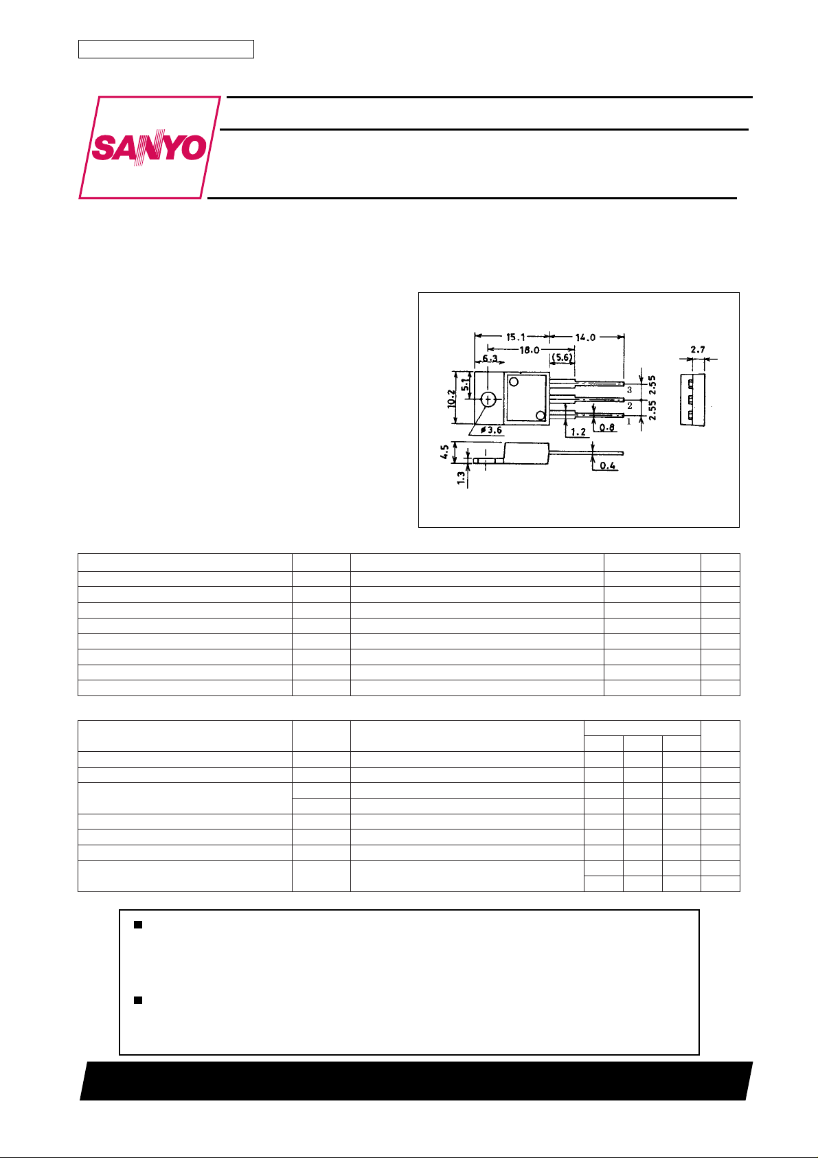
Package Dimensions
unit:mm
2010C
[2SB633/2SD613]
JEDEC : TO-220AB 1 : Base
EIAJ : SC-46 2 : Collector
3 : Emitter
OBC
OEC
OBE
Tc=25˚C
nimpytxam
V
OBC
OBE
BC
V
BE
V
EC
I
)tas(EC
C
I
E
V
BC
I,V04)–(=
0=1.0)–(Am
E
I,V4)–(=
0=1.0)–(Am
C
A1)–(=*04*023
C
A3)–(=02
C
I,V5)–(=
A1)–(=
C
I,A4)–(=
A4.0)–(=0.2)–(V
B
I,A5)–(=
A1)–(=5.1)–(V
C
zHM1=f,V01)–(=
001)–(V
58)–(V
6)–(V
6)–(A
01)–(A
04W
sgnitaR
51zHM
)051(Fp
011Fp
˚C
˚C
tinU
Any and all SANYO products described or contained herein do not have specifications that can handle
applications that require extremely high levels of reliability, such as life-support systems, aircraft’s
control systems, or other applications whose failure can be reasonably expected to result in serious
physical and/or material damage. Consult with your SANYO representative nearest you before using
any SANYO products described or contained herein in such applications.
SANYO assumes no responsibility for equipment failures that result from using products at values that
exceed, even momentarily, rated values (such as maximum ratings, operating condition ranges,or other
parameters) listed in products specifications of any and all SANYO products described or contained
herein.
SANYO Electric Co.,Ltd. Semiconductor Bussiness Headquaters
TOKYO OFFICE Tokyo Bldg., 1-10, 1 Chome, Ueno, Taito-ku, TOKYO, 110-8534 JAPAN
91098HA (KT)/90595MO (KOTO)/D251MH/4017KI/1115MW, TS/No.174, 8-2629 No.513–1/4
2SB633/2SD613
retemaraPlobmySsnoitidnoC
egatloVnwodkaerBesaB-ot-rotcelloCV
egatloVnwodkarBrettimE-ot-rotcelloC
egatloVnwodkaerBesaB-ot-rettimEV
emiTNO-nruTt
emiTllaFt
emiTegarotSt
V
V
I
OBC)RB(
C
I
OEC)RB(
C
I
OEC)RB(
C
I
OBE)RB(
E
no
f
gts
I,Am5)–(=
0=001)–(V
E
R,Am5)–(=
=∞ 58)–(V
EB
R,Am05)–(=
=∞ 58)–(V
EB
I,Am5)–(=
0=6)–(V
C
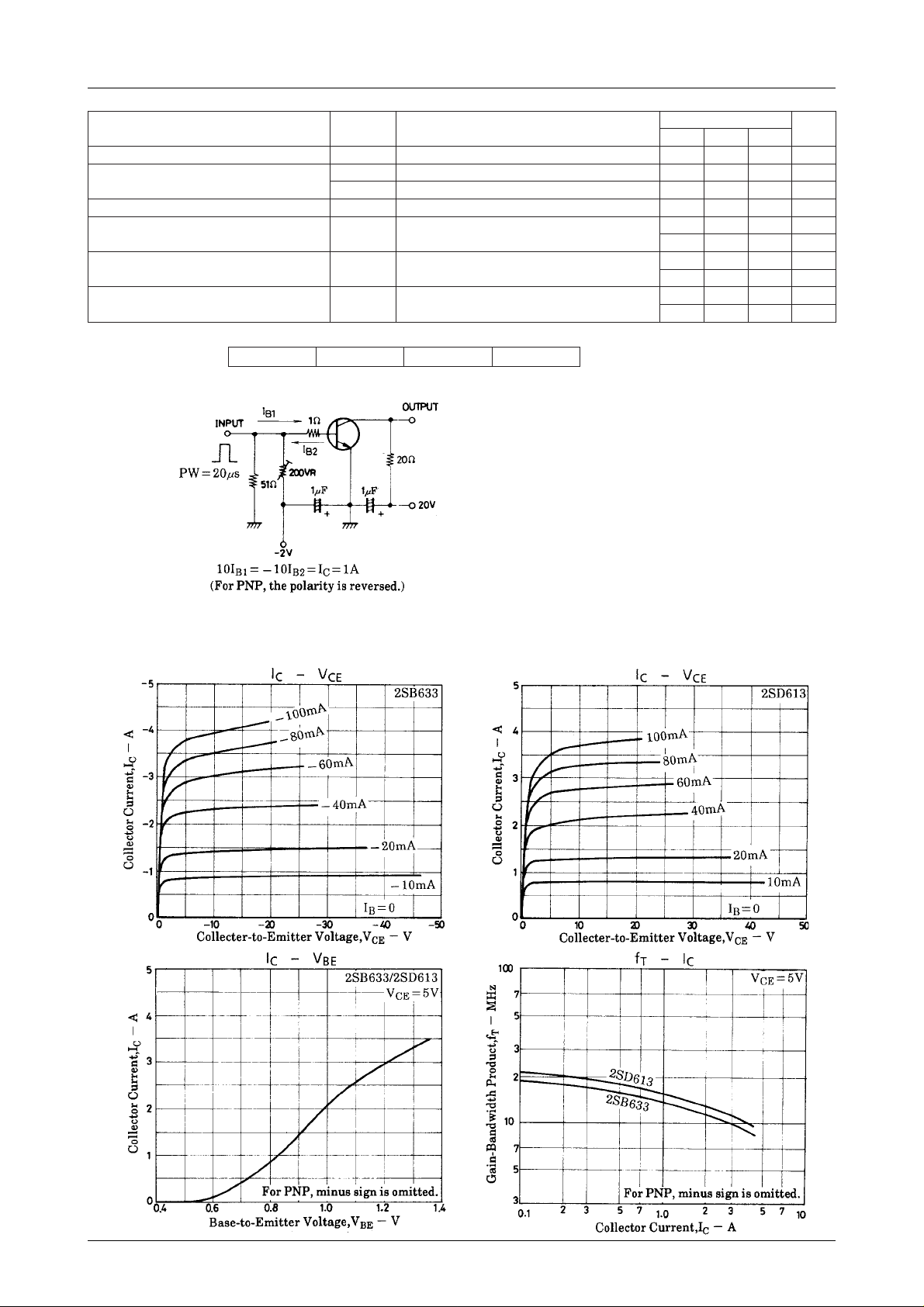
tiucriCtseTdeificepseeS
tiucriCtseTdeificepseeS
tiucriCtseTdeificepseeS
* : The 2SB633/2SD613 are classified by 1A hFE as follows :
08C04021D06002E001023F061
Switching Time T est Circuit
sgnitaR
nimpytxam
)61.0(sµ
82.0sµ
)33.0(sµ
05.0sµ
)54.1(sµ
06.3sµ
tinU
No.513–2/4
 Loading...