

SANYO 2SC5564, 2SA2011 Datasheet
Any and all SANYO products described or contained herein do not have specifications that can handle
applications that require extremely high levels of reliability, such as life-support systems, aircraft’s
control systems, or other applications whose failure can be reasonably expected to result in serious
physical and/or material damage. Consult with your SANYO representative nearest you before using
any SANYO products described or contained herein in such applications.
SANYO assumes no responsibility for equipment failures that result from using products at values that
exceed, even momentarily, rated values (such as maximum ratings, operating condition ranges,or other
parameters) listed in products specifications of any and all SANYO products described or contained
herein.
PNP/NPN Epitaxial Planar Silicon Transistors
DC/DC Converter Applications
Ordering number:ENN6305
2SA2011/2SC5564
SANYO Electric Co.,Ltd. Semiconductor Company
TOKYO OFFICE Tokyo Bldg., 1-10, 1 Chome, Ueno, Taito-ku, TOKYO, 110-8534 JAPAN
Applications
· Relay drivers, lamp drivers, motor drivers, strobes.
Features
· Adoption of MBIT processes.
· Large current capacitance.
· Low collector-to-emitter saturation voltage.
· High-speed switching.
· Ultrasmall-sized package permitting applied sets to
be made small and slim.
· High allowable power dissipation.
Specifications
( ) : 2SA2011
Absolute Maximum Ratings at Ta = 25˚C
retemaraPlobmySsnoitidnoCsgnitaRtinU
egatloVesaB-ot-rotcelloCV
egatloVrettimE-ot-rotcelloCV
egatloVesaB-ot-rettimEV
tnerruCrotcelloCI
)esluP(tnerruCrotcelloCI
tnerruCesaBI
noitapissiDrotcelloCP
erutarepmeTnoitcnuJjT 051
erutarepmeTegarotSgtsT 051+ot55–
Electrical Characteristics at Ta = 25˚C
retemaraPlobmySsnoitidnoC
tnerruCffotuCrotcelloCI
tnerruCffotuCrettimEI
niaGtnerruCCDh
tcudorPhtdiwdnaB-niaGf
ecnaticapaCtuptuOboCV
Marking : 2SA2011 : AR 2SC5564 : FA
OBC
OEC
OBE
C
PC
B
C
OBC
OBE
EF
T
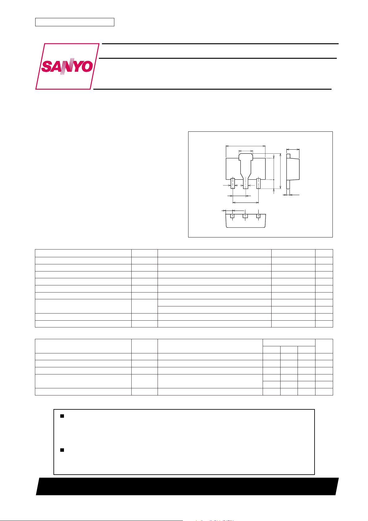
Package Dimensions
unit:mm
2038A
0.4
Mounted on a ceramic board (250mm
Tc=25˚C
V
BC
V
BE
V
EC
V
EC
BC
I,V21)–(=
0=1.0)–(Aµ
E
I,V4)–(=
0=1.0)–(Aµ
C
I,V2)–(=
C
I,V2)–(=
C
Am005)–(=002065
Am005)–(=
zHM1=f,V01)–(=
[2SA2011/2SC5564]
4.5
1.6
0.5
2
3
1.5
0.75
2
×0.8mm)
1
3.0
1.5
2.5
4.25max
1.0
0.4
1 : Base
2 : Collector
3 : Emitter
SANYO : PCP
(Bottom view)
sgnitaR
nimpytxam
)053(zHM
083zHM
32)14(Fp
Continued on next page.
51)–(V
51)21–(V
5)–(V
6)–(A
9)–(A
006)–(Am
3.1W
5.3W
˚C
˚C
tinU
21400TS (KOTO) TA-2519 No.6305–1/5
2SA2011/2SC5564
Continued on preceding page.
retemaraPlobmySsnoitidnoC
I
no
gts
f
C
)tas(
I
C
)tas(ICI,A5.1)–(=
I
OBC)RB(
C
I
OEC)RB(
C
I
OBE)RB(
E
egatloVnoitarutaSrettimE-ot-rotcelloCV
egatloVnoitarutaSrettimE-ot-esaBV
egatloVnwodkaerBesaB-ot-rotcelloCV
egatloVnwodkaerBrettimE-ot-rotcelloCV
egatloVnwodkaerBesaB-ot-rettimEV
emiTNO-nruTt
emiTegarotSt
emiTllaFt
EC
EB
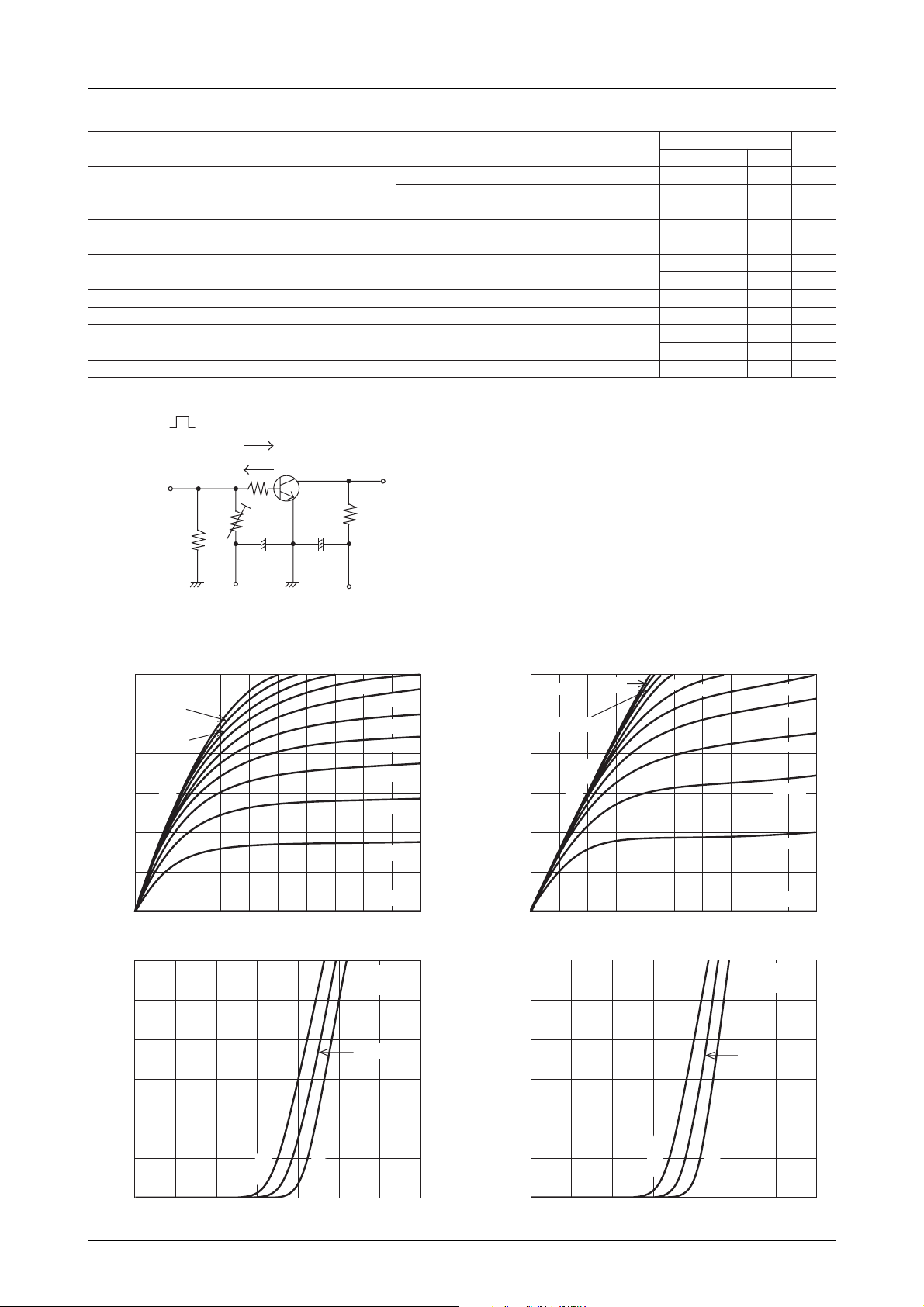
Switching Time Test Circuit
I,A5.1)–(=
B
I,A3)–(=
B
B
I,Aµ01)–(=
R,Am1)–(=
I,Aµ01)–(=
Am03)–(=
Am06)–(=
Am03)–(=58.0)–(2.1)–(V
0=51)–(V
E
=∞
EB
0=5)–(V
C
tiucriCtseTdeificepseeS
tiucriCtseTdeificepseeS
tiucriCtseTdeificepseeS
sgnitaR
nimpytxam
021)–(081)–(Vm
)091–()092–(Vm
002003Vm
)21–(V
51V
03)53(sn
)011(
091
51sn
tinU
sn
sn
V
R
100µF 470µF
VBE=--5V
I
I
B1
I
B2
R
C
B
+
-- V
CE
+
VCC=5V
--70mA
OUTPUT
R
L
--6
--5
–A
--4
C
--3
PW=20µs
D.C.≤1%
INPUT
50Ω
20IB1= --20IB2= IC=1.5A
(For PNP, the polarity is reversed.)
2SA2011
--90mA
--80mA
--100mA
--2
Collector Current, I
--1
0
0 --0.2 --0.4 --0.6 --0.8 --1.0
Collector-to-Emitter Voltage, VCE–V
I
-- V
--6
C
BE
2SA2011
VCE=--2V
--5
--60mA
--
50mA
--
40mA
--30mA
--20mA
--10mA
IB=0
IT00115
6
5
–A
4
C
3
2
2SC5564
80mA
C
90mA
100mA
70m
A
CE
60mA
I
-- V
Collector Current, I
1
0
0 0.2 0.4 0.6 0.8 1.0
Collector-to-Emitter Voltage, VCE–V
I
-- V
6
C
BE
2SC5564
VCE=2V
5
50mA
40mA
30mA
20mA
10mA
IB=0
IT00116
–A
--4
C
--3
--2
Collector Current, I
--1
0
0 --0.2 --0.4 --0.6 --0.8 --1.4--1.0 --1.2
Base-to-Emitter Voltage, VBE–V
°C
Ta=75
°C
--25
25°C
IT00117
–A
4
C
3
2
Collector Current, I
1
Ta=75°C
0
0 0.2 0.4 0.6 0.8 1.41.0 1.2
Base-to-Emitter Voltage, VBE–V
°C
--25
25°C
IT00118
No.6305–2/5
 Loading...