

SANYO 2SA1973 Datasheet
Any and all SANYO products described or contained herein do not have specifications that can handle
applications that require extremely high levels of reliability, such as life-support systems, aircraft’s
control systems, or other applications whose failure can be reasonably expected to result in serious
physical and/or material damage. Consult with your SANYO representative nearest you before using
any SANYO products described or contained herein in such applications.
SANYO assumes no responsibility for equipment failures that result from using products at values that
exceed, even momentarily, rated values (such as maximum ratings, operating condition ranges,or other
parameters) listed in products specifications of any and all SANYO products described or contained
herein.
PNP/NPN Epitaxial Planar Silicon Transistors
DC/DC Converter Applications
Ordering number:ENN5613
2SA1973/2SC5310
SANYO Electric Co.,Ltd. Semiconductor Company
TOKYO OFFICE Tokyo Bldg., 1-10, 1 Chome, Ueno, Taito-ku, TOKYO, 110-8534 JAPAN
0.4
Features
· Adoption of FBET, MBIT processes.
· Large current capacitance.
· Low collector-to-emitter saturation voltage.
· High-speed switching.
· Ultrasmall package facilitates miniaturization in end
products.
Specifications
( ) : 2SA1973
Absolute Maximum Ratings at Ta = 25˚C
retemaraPlobmySsnoitidnoCsgnitaRtinU
egatloVesaB-ot-rotcelloCV
egatloVrettimE-ot-rotcelloCV
egatloVesaB-ot-rettimEV
tnerruCrotcelloCI
)esluP(tnerruCrotcelloCI
tnerruCesaBI
noitapissiDrotcelloCP
erutarepmeTnoitcnuJjT 051
erutarepmeTegarotSgtsT 051+ot55–
OBC
OEC
OBE
C
PC
B
Mounted on a glass-epoxy board (20×30×1.6mm)
C
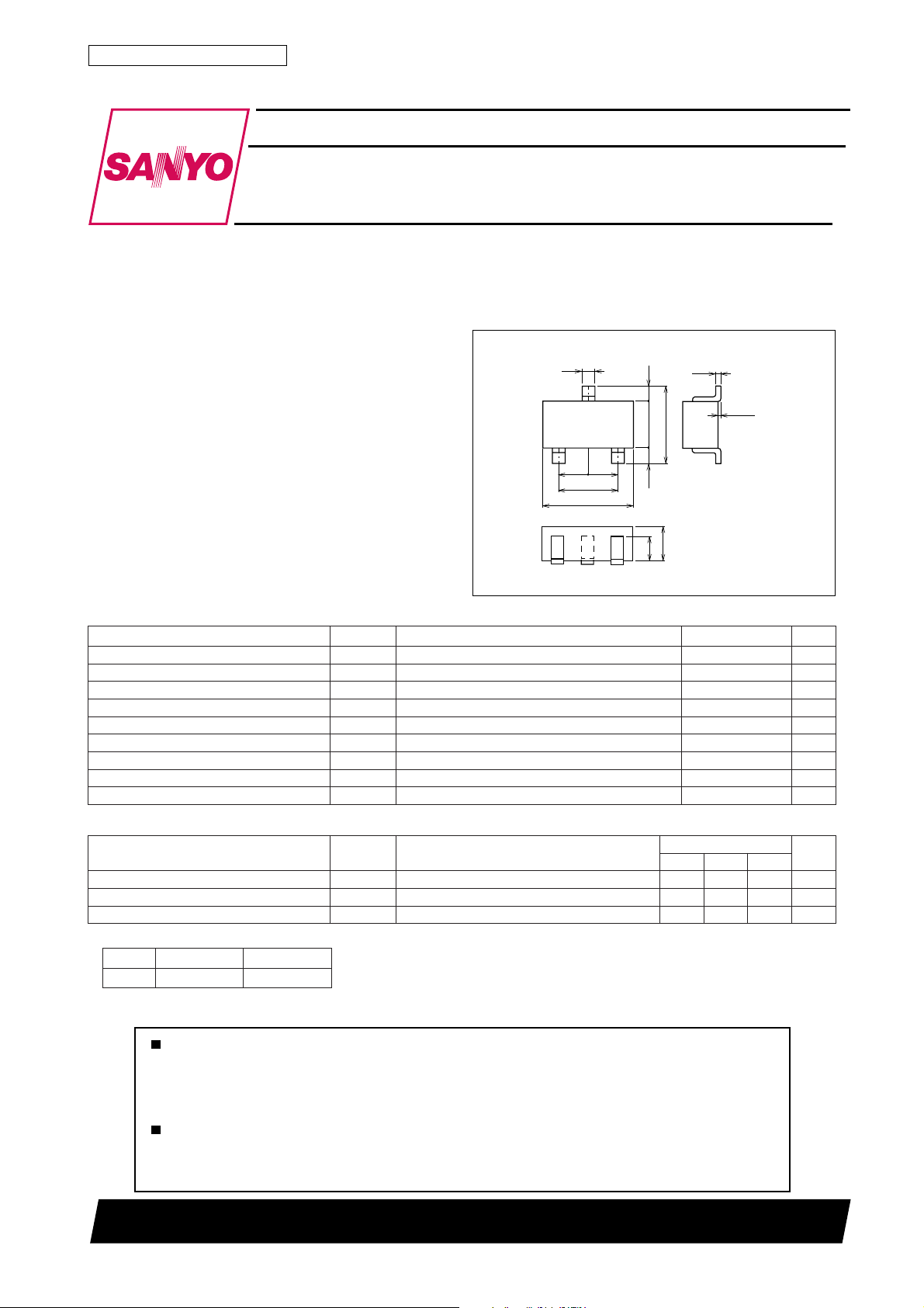
Package Dimensions
unit:mm
2018B
[2SA1973/2SC5310]
3
1
0.95
0.95
1.9
2.9
0.5
1.5
2
0.5
0.8
0.16
2.5
0 to 0.1
1 : Base
1.1
2 : Emitter
3 : Collector
SANYO : CP
03)–(V
52)–(V
6)–(V
1)–(A
3)–(A
002)–(Am
052Wm
˚C
˚C
Electrical Characteristics at Ta = 25˚C
retemaraPlobmySsnoitidnoC
tnerruCffotuCrotcelloCI
tnerruCffotuCrettimEI
niaGtnerruCCDh
V
OBC
OBE
EF
BC
V
BE
V
EC
I,V02)–(=
0=1.0)–(Aµ
E
I,V3)–(=
0=1.0)–(Aµ
C
I,V2)–(=
C
Am001)–(=*531*004
nimpytxam
* : The 2SA1973/2SC5310 are classified by 100mA hFE as follows : Continued on next page.
knaR5 6
h
EF
072ot531004ot002
Marking : 2SA1973 : NS
2SC5310 : NN
60100TS (KOTO) TA-1556 No.5613–1/4
sgnitaR
tinU
2SA1973/2SC5310
Continued on preceding page.
retemaraPlobmySsnoitidnoC
tcudorPhtdiwdnaB-niaGf
ecnaticapaCtuptuOboCV
egatloVnoitarutaSrettimE-ot-rotcelloCV
egatloVnoitarutaSrettimE-ot-esaBV
egatloVnwodkaerBesaB-ot-rotcelloCV
egatloVnwodkaerBrettimE-ot-rotcelloCV
egatloVnwodkaerBesaB-ot-rettimEV
emiTNO-nruTt
emiTegarotSt
emiTllaFt
Switching Time Test Circuit
I
V
R
B1
I
B2
1kΩ
+
100µF 470µF
R
+
OUTPUT
L
PW=20µs
D.C.≤1%
INPUT
50Ω
T
EC
EB
no
gts
f
V
EC
BC
)tas(I
C
)tas(I
C
I
OBC)RB(
C
I
OEC)RB(
C
I
OBE)RB(
E
I,V01)–(=
C
I,Am005)–(=
I,Am005)–(=
I,Aµ01)–(=
E
R,Am1)–(=
I,Aµ01)–(=
C
Am05)–(=051zHM
zHM1=f,V01)–(=91)23(Fp
B
B
EB
Am52)–(=
Am52)–(=58.0)–(2.1)–(V
0=03)–(V
=∞ 52)–(V
0=6)–(V
tiucriCtseTdeificepseeS
tiucriCtseTdeificepseeS
tiucriCtseTdeificepseeS
sgnitaR
nimpytxam
)051–()003–(Vm
001002Vm
06)06(sn
)053(
005
52)52(sn
tinU
sn
sn
VBE=--5V
20IB1= --20IB2= IC=500mA
(For PNP, the polarity is reversed.)
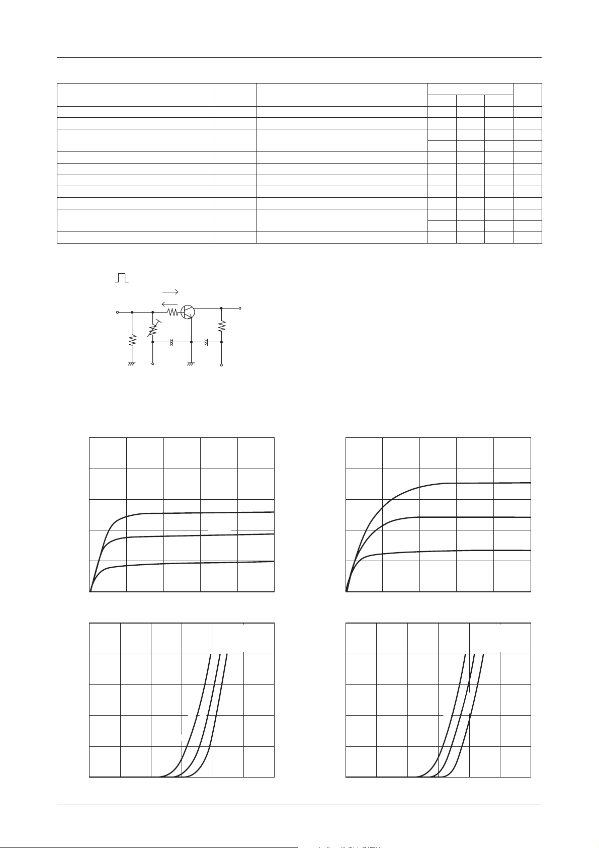
I
--1.0
--0.8
C
–A
C
--0.6
--0.4
Collector Current, I
--0.2
0
0 --0.8 --2.0--1.6--0.4 --1.2
Collector-to-Emitter Voltage, VCE–V
I
--1000
--800
C
-- V
-- V
CE
BE
VCC=12V
--6mA
--4mA
--2mA
=0
I
B
2SA1973
Pulse
ITR08234
2SA1973
VCE=--2V
Pulse
I
1.0
0.8
C
–A
C
0.6
0.4
Collector Current, I
0.2
0
0 0.8 1.6 2.00.4 1.2
Collector-to-Emitter Voltage, VCE–V
I
1000
800
C
-- V
-- V
CE
BE
6mA
4mA
2mA
I
B
2SC5310
Pulse
=0
ITR08235
2SC5310
VCE=2V
Pulse
–mA
C
--600
--400
Collector Current, I
--200
0
0 --0.2 --0.4 --0.6 --0.8 --1.2--1.0
°C
Ta=75
°C
25
Base-to-Emitter Voltage, VBE–V
--25°C
ITR08236
–mA
C
600
°C
25°C
400
Collector Current, I
200
0
0 0.2 0.4 0.6 0.8 1.21.0
Ta=75
Base-to-Emitter Voltage, VBE–V
°C
--25
ITR08237
No.5613–2/4
 Loading...