


AU-517
AU-
.....................
. . . . . . . . . . . . . . . . . . .
. . . . . . . . . . . .
. . . . . . . . .
...............
. . . . . . . . .
...........
. . . . . . . . . . . . . . .
. . .
517/717
. . . ..
. . . . .
-"'"""~~,, . ,"-"-,
"" :~ ,~ ,~ ,
~ ~
-- --- -----,,-------
""
~: g~
.:.:
- - - - -- ---
:_---------+ _
$; ~'"" ~ ';;~~: , , ,"- "- ,-- --.,.
~ ""
--- ---- --~ -~--~--_!_--_
"'"
,'j,- - - - - --';",
----------
---- -- -.. ~:
- -----_
1. SPCIFICA TlaNS
AU-717
Power output
Min. RMS, both channels driven, from 20 to 20
more than 0.025% total harmonic distortion
Load impedance.
Power bandwidth.
Total harmonic distortion
Intermodulation distortion (70 Hz: 7 kHz = 4:1 SMPTE method)
Frequency response (at 1watt) (POWER AMP IN)
..................,.. Oto200 OOOHz+OdB-3dB
RIAA curve daviation
Damping factor.
Input sensitivity and impedance
PHONO "
(Max. input capability; 350 mV at 1 kHz
harmonic distortion)
AUX, TAPE. . . . . . . . .
Output level (1 ,000 Hz)
TAPEREC(pinjack) "
PREOUT
Channel separation (1 kHz
PHONO "
AUX..................
Hum and noise
PHONO ..........
AUX..............
Controls
BASS.
Tone selector
TREBLE
Toneselector...........
SUBSONIC
HIGHFILTER............
MUTING
LOUDNESS (-30dB) .,.
Power requirements
Powervoltage............. 100
Power consumption
Maximum consumption. .
Rated consumption
Dimentions................
Waight
85 watts per channel into 8. ohms
'...........,.... lessthanO.025%
(short-circuit, A-network)
FILTER.........
. . . . . . . . 8 ohms
(POWER AMP IN)
(PHONO) . . . . +0.2 dB - 2 dB
, at rated power output)
20 to 20
rated min. RMS power output
and total harmonic distortion
less than 0.025% at or below
rated min. RMS power output
(20 to 20 000 Hz)
approximately 60 at 8 ohms
load
, for rated power output)
(1 kHz
" 2.
5mV/47kilohms
150mV/47 kilohms
150mV/47kilohms
1V/47kilohms
betterthan60dB
betterthan65dB
78dB
100dB
:!:10dB (50 Hz)
200 400 Hz
:!:10dB (15kHz)
, 6 kHz
3dB(16Hz),
3dB (10kHz), 6dB/oct
20dB
9dB at 50Hz
7dBat10kHz
, 120
120V (Usable 110 - 130V)
60 Hz (for U. A. & Canada
only)
735 watts
425 watts 500 VA
430mm (16-
168 mm (6-5/8"
389mm (15-3/8") D
8kg (39.2lbs) net
19.8 kg (43.7 Ibs) packed
000 Hz, with no
000 Hz at or below
, less than 0.01 % total
6dB/oct
220
240V (50/60Hzl
15/16") W
) H
2.
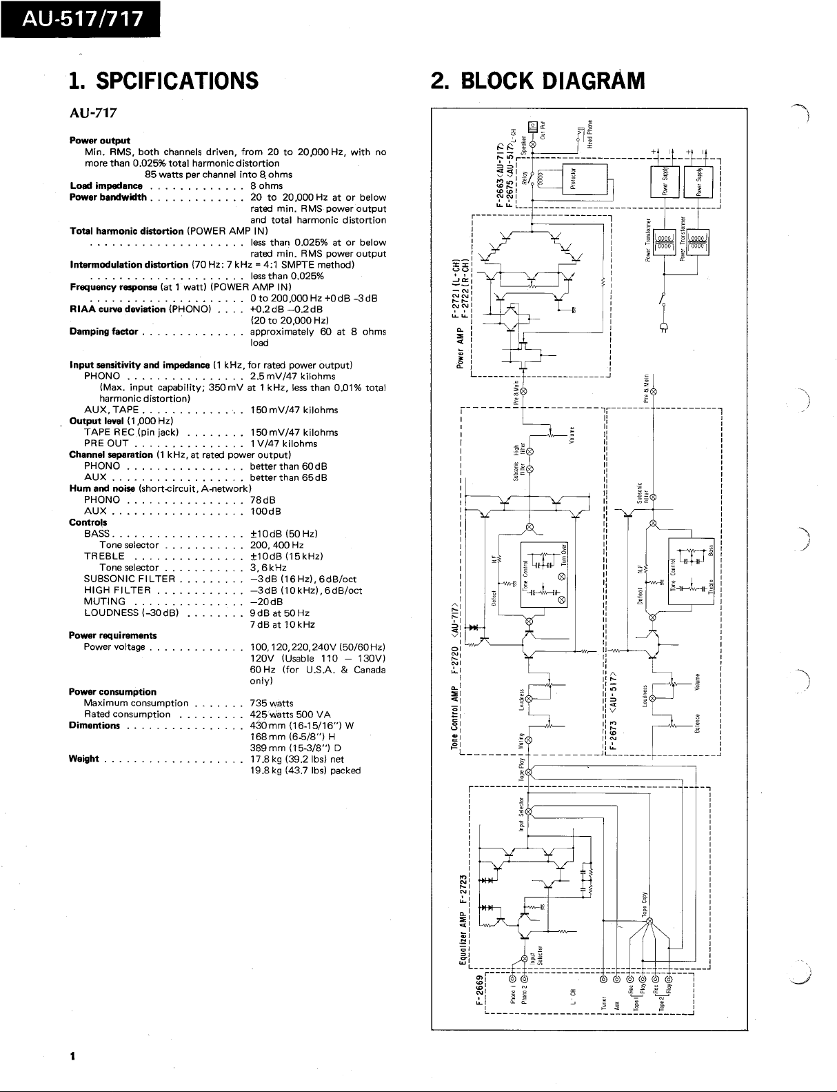
BLOCK DIAGRAM
0 ~
7'"
t --------_
:i!!:i!!, -
r----____n
:r:t: I
UUI
, 'I
--' a: I
0.. I
'" I
0.. I
Ln_____-
"'I
":"1
0..
""I
:: I
:51
,21
L______--
r--------- ---------------------
n_____------
_n_______n__-
;;'1 ~
, I ~
IIA
JlI'-
Ii;;;
II,
JI'"
I:~
I:~
"(0
d ..:..
JL______-
n__----_n
ttJ~
1'-'
"'I
..:..' u
0..
I ~
"" I
~I
"gl
=1
~I
L______- - ------------- -- - -- - -
~r----
(0 -(0 -------------
i'i~
L__- -- - --
"C0 -(0"-
&ii&ii
- c0~---
... '-'
........ ........
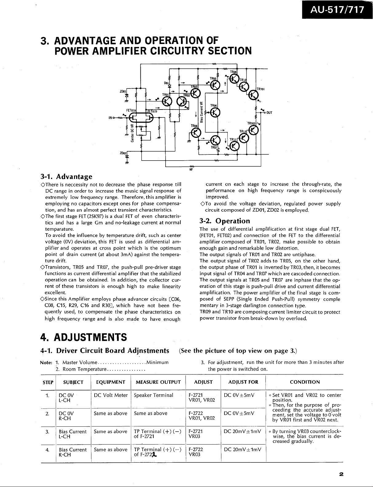
ADVANTAGE AND OPERATION OF
3.
POWER AMPLIFIER CIRCUITRY SECTION
DOl
ZDOI
FETOl"
ZDO2
AU-
517/717
1. Advantage
OThere is neccessity not to decrease the phase response till
DC range in order to increase the music signal response of
extremely low frequency range. Therefore, this amplifier is
employing no capacitors except ones for phase compensa-
tion, and has an almost perfect transient characteristics.
0 The first stage
tics and has a large Gm and no-
FET (2SK9?) is a dual FET of even characteris-
leakage current at normal
temparature.
To avoid the influence by temperature drift
voltage (OV) deviation
, this FET is used as differential am-
plifier and operates at cross point which is the
point of drain current (at about
3mA) against the tempera-
, such as center
optimum
ture drift.
OTransistors
, TROS and TRO?
, the push-pull pre-
driver stage
functions as current differential amplifier that the stabilized
operation can be obtained. In addition
rent of these transistors is enough high to make
, the collector cur-
linearity
excellent.
OSince this Amplifier employs phas~ advancer circuits (CO6
COB, C1S, R29
quently used
high frequency range and is also made to
, C16 and R30J, which have not
, to
compensate the phase characteristics on
have enough
been fre-
4. ADJUSTMENTS
1. Driver Circuit Board Adjnstments
current on each stage to increase the through-rate
performance on high frequency range is conspicuously
improved.
OTo avoid the
circuit composed of ZDO1, ZDO2 is employed.
2. Operation
The use of differential amplification at first stage dual FET
(FETO1 , FETO2) and connection of the FET to the
amplifier composed of TRO1
enough gain and remarkable low distortion.
The output signals of TRO1 and TRO2 are untiphase.
The output signal of
the output phase of TRO1 is inverted by TRO3
input signal of TRO4 and TRO? which are cascoded connection.
The output signals at
eration of this stage is push-
amplification. The power amplifier of the final stage is com-
posed ofSEPP
mentary in 3-
TRO9 and TR10 are
power transistor from break-
(See
the picture of top view on page
voltage deviation, regulated power supply
differential
, TRO2
, make possible to obtain
TRO2 adds to TROS
TROS and TRO? are
pull drive and current differential
, on the other hand
, then, it becomes
inphase that the op-
(Single Ended Push-Pull) symmetry comple
stage darlington connection type.
composing current limiter circuit to protect
down by overload.
, the
Note: 1.
STEP I
Master Volume....
RoomTemperature................
SUBJECT I EQUIPMENT
DCOV
L-CH
DCOV Same as above
DC Volt Meter Speaker Terminal
Bias Current Same as above
Bias Current
Same as above
I MEASURE
Minimum
OUTPUT I
Same as above F-2722 DC OV:tSmV
TP Terminal (+) (-)
of F-2721 VRO3 wise, the bias current is de-
TP Terminal (+) (-) F-2722 DC 20mV:t1mV
of F-2?~
3. For adjustment
the power is switched on.
ADJUST
F-2721 DC OV:tSmV
VRO1, VRO2
VRO1, VRO2
F-2721 DC 20mV:t1mV
VRO3
, run the unit for more than 3 minutes after
ADJUST FOR CONDITION
0 Set VRO1 and
position.
0 Then
, for the purpose of pro-
ceeding the accurate adjust-
, set the voltage to 0 volt
ment
by VRO1 first and VRO2 next.
0 By turning
creased gradually.
VRO2 to center
VRO3 counterclock-
AU-
517/717
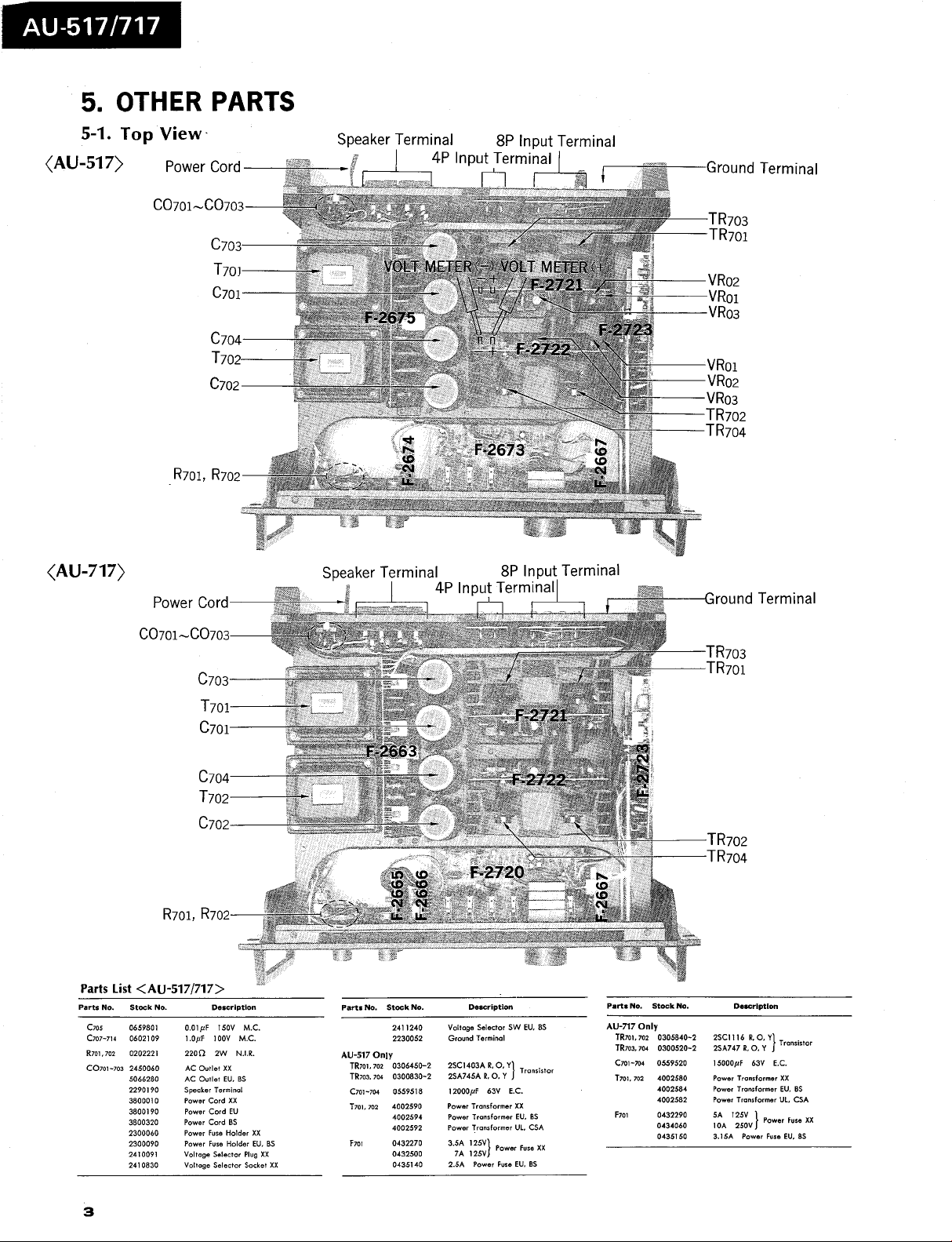
5. OTHER PARTS
1. Top View'
(AU-517)
717)
(AU-
Power Cord
CO701-CO703
C703
T70J
C701
C704
T702
C702
R701, R702
Power Cord
Speaker Terminal
4P Input Terminal
Speaker Terminal
4P Input Terminal
8P Input Terminal
Ground Terminal
TR703
TR701
VR02
VR01
VR03
VR01
VR02
VR03
TR702
TR704
8P Input Terminal
round Terminal
CO701-
CO703
C703
T701
C701
C704
T702
C702
R701, R702
Parts List ~AU-517/717?
Parts No.
Stock No.
ClO5
0659801
C707-714
0602109
R701,7O2
0202221
C0701-7O3 2450060
5066280
2290190
3800010
3800190
3800320
2300060
2300090
2410091
2410830
OlpF 150V M.
1.0pF 100V M.
2200 2W NH.
AC 0,11., XX
AC 0",., EU,
Sp.ok., r.,m;"ol
Pow., Co,d XX
Pow., Co,d EU
Pow., COld 85
Pow., F". Hold.,
Pow., F". Hold., EU. 85
Vollog. S.I.clOt Pl'g XX
Vol log. S.I.ctOl Sock.' XX
Description
Parts No. Stock
2411240
2230052
AU-517 OnlY
TR701.702 0306450-
TR703, 704 0300830-2
C701-704 0559518
4002590
T701.702
4002594
4002592
F7O1 0432270
0432500
0435140
No.
Voltage S.I.cto' SW EU. 85
Gm""d r.,ml"ol
2SCI403AR,
2SA745A R, 0, Y
12000pF 63V E.
Pow., r,o",10,m., XX
Pow., r,0",10,m.,
Pow., r,o",10,m., Ul. CSA
5A 125V
7A 125V ow., ".
5A
Description
Pow., F". EU, 85
r,o","'o,
EU. 85
Parts No. Stock No.
AU-717 Only
TRlOI,
7O2 0305840-2
TRlO3,704 0300520-2
ClOt-704 0559520
T7OI,7O2 4002580
4002584
4002582
F70t 0432290
0434060
0435150
TR703
TR701
TR702
TR704
Description
2SCI116R,
2SA747 R, 0, Y
15000pF 63V E.
Pow., r,o"do,m., XX
Pow., r,o",fo,m., EU. 85
Pow., r,o",fo,m., Ul. CSA
5A 125V
lOA 250V Pow., F".
15A Pow., F". EU.
r,o",I,'o'
AU-517/717
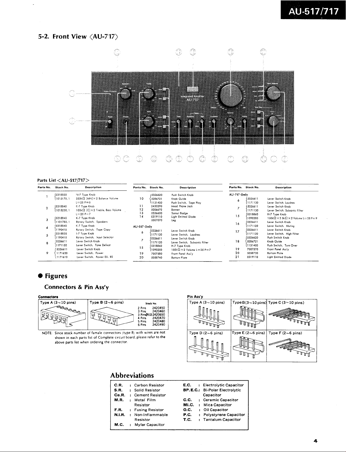
2. Front View
Parts List ~AU-517/717/
P."s No.
Stock No.
1015170.
15318850
1015230.
15318840
1101780.
15318840
1190410
15318840
1190410
15318830
1171150
15326611
1171630
1171610
r326611
7 Type Koob
250kO (MN)x2 80'00" Vo"me
L=25 P=5
7 Type Koob
100'0 (C)x2 T,eb". 80", Vol,m,
L=25 P=7
7 Type Koob
'Olo,y Switch, Sp,ok",
7 Type Koob
'oto,y Switch. Top' Copy
7 Typa Koob
'otOty SwiJ,h. 'op" Sel,"ot
Le"t Switch Koob
L"" Switch, Tooe Del,ot
L"" Switch
La,et Switch. Pow"
L"e' SwiJd.
(AU-
Descdpt;on
Koob
Powat EU. 8S
717)
P.", No. Stock No.
(326620 P"h Switch Koob
5286721 Koob G,ide
1131400 P"h Switch.
2430290
5006670 8000ot
5336600 So",,, 80dge
0319110 light Emitt,d Dioda
5507070
AU-S17 Only
1171120 Le,et Switch, Lo,doe,
15326611
11 711 20 Le", Switch,S,b,ooic Filtet
15326611
1 090250 150,OX2Vol,meL=25P=7
15318860
7007580 FtC" Pooel A"y
5058740 80ttom Plote
De,cdpt;on
Haod Phooe Jock
Leg
Le,et Switch Koob
L"" SwiJd Koob
Top, Ploy
7 Typa Koob
P.", No.
Stock No. De,c';pt;on
AU-717 Only
!5326611
11 71130
!532661 I L"" SwiJ,h
1171130
1090280 150l0 x2 5kO x 2VoI,me L=25 P=9
15318860
1171120 Le", Switch.M,tiog
15326611
1171130 Le'at SwiJd,
15326611
5286721 Koob G,ide
1131400
r326620
7007570 Fto" Pooal A"y
5058730 80ttom Plote
0319110
Le"t Switch Koob
L"" SwiJd. Lo,do"
Koob
L"" Switch. S,b,oo', Filt"
7 Type Koob
Le'et SwiJd Koob
Le"t Switd
P"h Switch Koob
P"h SwiJch.
Light Emitt,d Diode
Koob
High Filtet
T"o 0",
. Figures
Connectors & Pin Ass
Connectors
Type A (3-10 pins)
NOTE: Since stock number of Jamale connectors (type
shown in each parts list of Complete crrcUit board
above parts list when ordering the connector.
Type B (2-6 pins)
Abbreviations
Ce.
Slock No.
2 p,ns 2420450
3 Pins 2420460
3 P'n~ED) 2420650
4 PInS 2420470
5 Pins 2420480
6 PInS 2420490
61 with wires are not
, please refer to the
: Carbon Resistor
: Solid Resistor
: Cement Resistor
: Metal Film
Resistor
: Fusing Resistor
: Non.lnflammable
Resistor
: Mylar Capacitor
Pin Ass
Type A (3-10 pins) TypeB(3-10 pins) Type C (3-10 pins)
Type D (2-6 pins)
Type E (2-
6 pins)
C. : Electrolytic Capacitor
BP. : Bi. Polar Electrolytic
Mi.
Capacitor
: Ceramic Capacitor
: Mica Capacitor
: Oil Capacitor
: Polystyrene Capacitor
: Tantalum Capacitor
 Loading...