Sanken Electric Co TM1661B-L, TM1641B-L Datasheet

TO-3PF 16A Triac
TM1641B-L, TM1661B-L
■Features
●Repetitive peak off-state voltage: V
●RMS on-state current: I
●Gate trigger current: I
●
Rate-of-rise of off-state commutation voltage
●Isolation voltage: V
GT
=2000V(AC, 1min.)
ISO
=16A
T(RMS)
=30mA max (MODE , , )
●UL approved type available
=400, 600V
DRM
: (dv/dt)c=10V/µs min.
■Absolute Maximum Ratings
Parameter Symbol
Repetitive peak off-state voltage
RMS on-state current
Surge on-state current
Peak gate voltage
Peak gate current
Peak gate power loss
Average gate power loss
Junction temperature
Storage temperature
Isolation voltage
V
DRM
I
T(RMS)
I
TSM
V
GM
I
GM
P
GM
P
G(AV)
Tj
Tstg
V
ISO
TM1641B-L
400
Ratings
160
–40 to
–40 to
2000
TM1661B-L
16
10
2
5
0.5
+
125
+
125
600
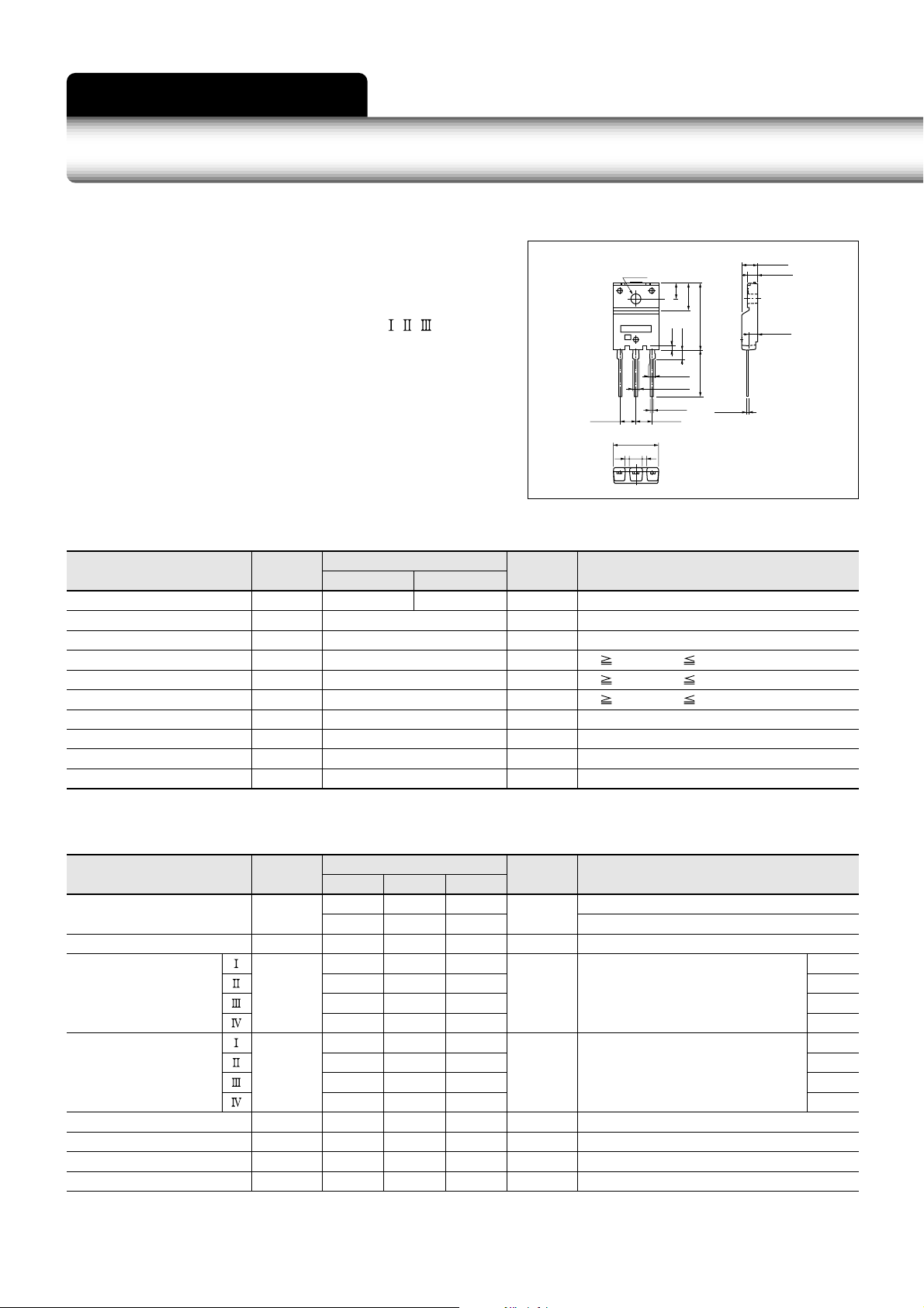
External Dimensions
(Unit: mm)
5.45
3.2
a
b
±
0.1
15.6
1.5 4.4 1.5
(1) (2) (3)
0.2
±
0.2
0.2
±
±
5.5
9.5
0.3
±
23
1.6
3.3
+0.2
0.1
–
1.75
+0.2
(16.2)
0.1
–
2.15
+0.2
0.1
–
1.05
5.45
0.2
±
±
0.1
0.65
(1). Terminal 1 (T1)
(2). Terminal 2 (T2)
(3). Gate (G)
Unit Conditions
V
A
A
V
A
W
Conduction angle 360°, Tc=92.5°C
50Hz full-cycle sinewave, Peak value, Non-repetitive, Tj=125°C
f 50Hz, duty 10%
f 50Hz, duty 10%
f 50Hz, duty 10%
W
°C
°C
Vrms
50Hz Sine wave, RMS, Terminal to Case, 1 min.
0.2
±
5.5
0.2
±
3.45
0.2
±
3.35
+0.2
0.1
–
a. Part Number
b. Lot Number
Weight: Approx. 6.5g
■Electrical Characteristics
Parameter Symbol
Off-state current
On-state voltage
Gate trigger voltage
Gate trigger current
Gate non-trigger voltage
Holding current
Rate-of-rise of off-state commutation voltage
Thermal resistance
48
I
DRM
V
V
I
V
Rth
TM
GT
GT
GD
I
H
0.2
10
Ratings
typmin max
0.1
0.8
0.7
0.8
1.0
12
16
25
70
25
Unit Conditions
2.0 V
0.1
1.6
mA
V
1.5
1.5
1.5
V
30
30
30
mA
V
mA
V/µs(dv/dt)c V
1.8
°C
/W
=
V
, R
D
DRM
GK
V
=
V
, R
D
DRM
GK
I
=
20A, T
°C
L
L
C
=
=
DRM
=
10Ω, T
10Ω, T
TM
V
=
6V, R
D
V
=
6V, R
D
V
=
1/2×V
D
=
25
Tj
=
400V, Tj=125
D
Junction to case
=
, Tj=125
∞
=
, Tj=25
∞
25
°C
C
C
, Tj=125
°C
°C
°C
+
+
T
, G
2
+
–
T
, G
=
25
°C
=
25
°C
2
–
–
T
, G
2
–
+
T
, G
2
+
+
T
, G
2
+
–
T
, G
2
–
–
T
, G
2
–
+
T
, G
2
°C

v
–
i
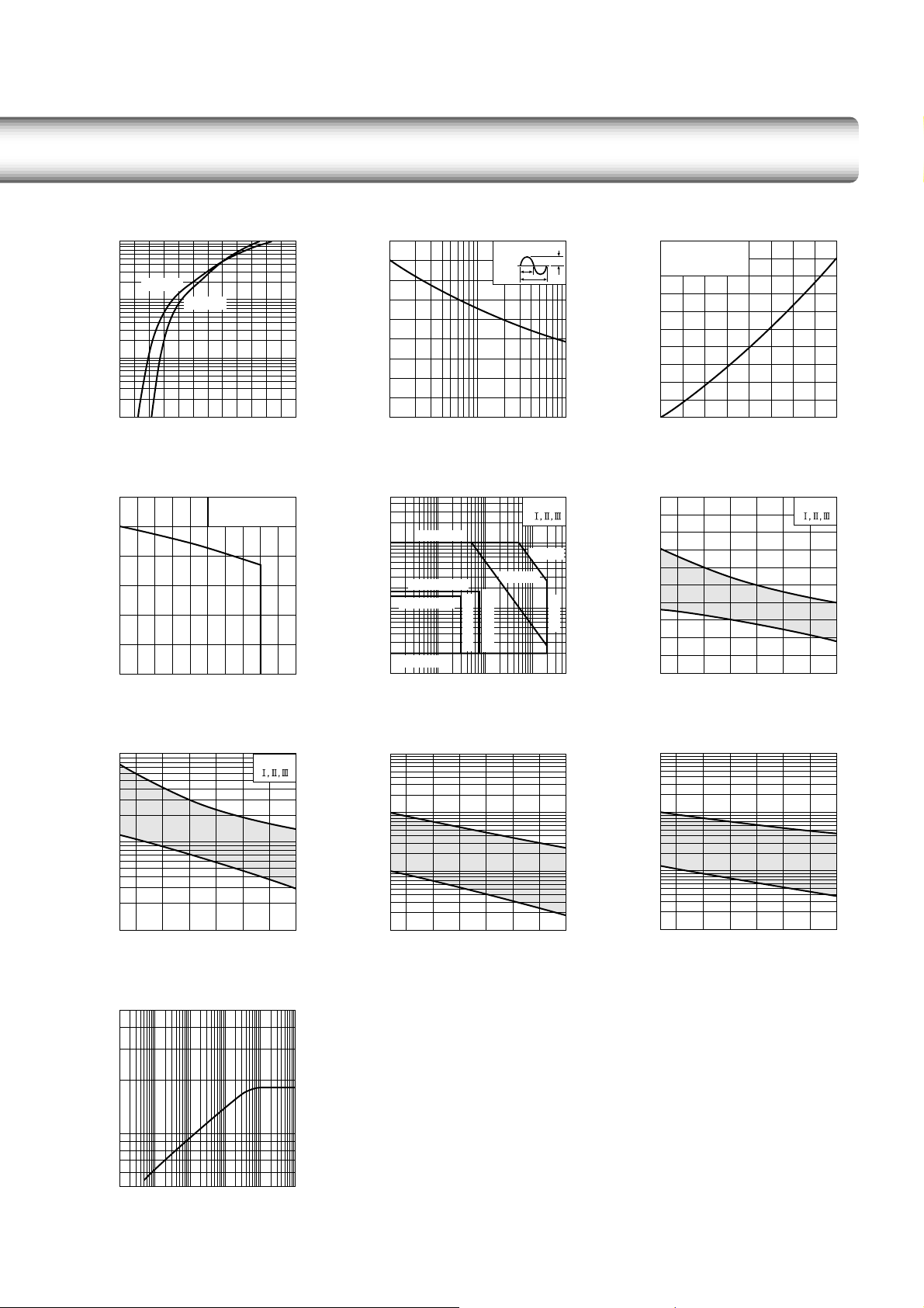
Characteristics (max)
T
T
100
(A)
T
On-state current i
I
T(RMS)
(°C)
C
Case temperature T
Tj=125°C
0.1
10
1
0.4
Tj= 25°C
0.8 1.2 2.0 2.41.6 2.8
v
On-state voltage
(V)
T
– Tc Ratings
150
125
100
75
50
25
0
048121620
RMS on-state current I
Full-cycle sinewave
Conduction angle: 360°
)
T(RMS
(A)
I
Ratings
TSM
180
160
(A)
140
TSM
120
100
80
60
40
Surge on-state current I
20
0
1 5 10 50 100
Number of cycle
Initial junction temperature
Tj=125°C
10 ms
1cycle
Gate Characteristics
50
VGM=10V
10
(V)
GF
=30mA
GT
25°C I
P
=75mA
GT
–40°C I
i
GF
–40°C V
=1.8V
GT
25°C V
=1.5V
GT
1
Gate voltage v
VGD=0.2V
0
101 100 1000 5000
Gate current
TM1641B-L, TM1661B-L
G(AV
(mA)
=0.5W
)
Mode
PGM=5W
I
T(RMS)–PT(AV)
20
I
TSM
=2A
GM
I
Full-cycle sinewave
Conduction angle: 360°
(W)
)
16
AV
(
T
12
8
4
Average on-state power P
0
0481216
V
temperature characteristics
GT
(Typical)
2.0
1.6
(V)
GT
1.2
0.8
0.4
Gate trigger voltage V
0
Characteristics
RMS on-state current I
0–40 –25 25 50 75 100 125
Junction temperature Tj (°C)
(V
T(RMS
=6V R
D
(A)
)
=10 Ω)
L
Mode
I
temperature characteristics
GT
(Typical)
100
50
10
5
Gate trigger current IGT (mA)
1
r
th( j-c) –t
5
(°C/W)
th (j-c)
1
0 25 50 75 100 125
Junction temperature Tj (°C)
Characteristics
(V
=6V R
D
=10 Ω)
L
Mode
I
temperature characteristics
H
(Typical)
1000
(mA)
100
H
10
Holding current I
1
0 25 50 75 100 125
Junction temperature Tj (°C)
I
temperature characteristics
L
(R
=1kΩ)
G-K
(Typical)
1000
(mA)
100
L
10
Latching current I
1
0–40 –25–40 –25–40 –25 25 50 75 100 125
Junction temperature Tj (°C)
(R
=∞)
G-K
Transient thermal resistance r
0.5
3
2
10
10
101
t, Time (ms)
5
4
10
10
49
 Loading...