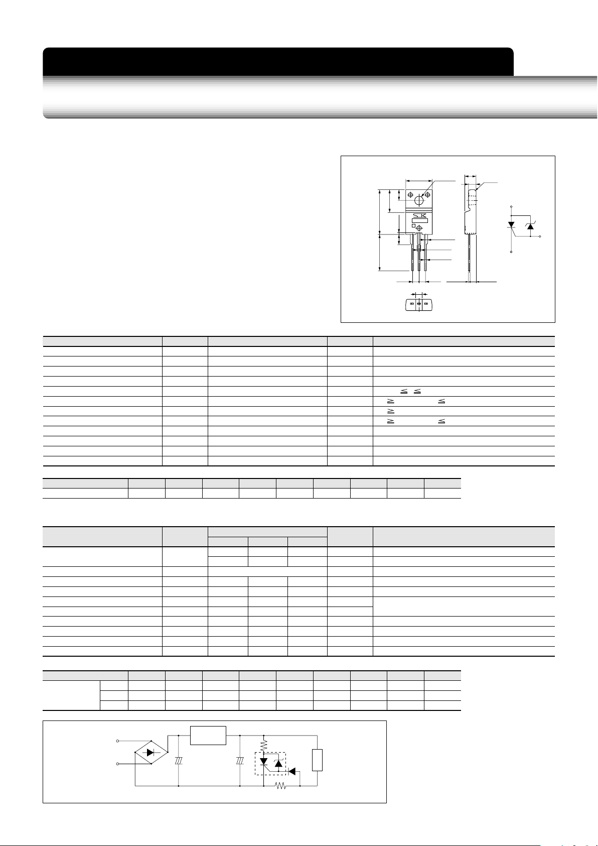
Sanken Electric Co TFD312S-G Datasheet

■Absolute Maximum Ratings
■Electrical Characteristics
✽V
DRM
✽V
BO
Parameter Symbol
Ratings
Unit Conditions
V
50Hz Half-cycle sinewave, 180°, Continuous current, Tc =92°C
50Hz Half-cycle sinewave, Peak value, Non-repetitive, Tj=125°C
50Hz Sine wave, RMS, Terminal to case, 1min.
(
Tj=25°C, unless otherwise specified)
A
A
V
V
W
W
°C
°C
V
V
DRM
I
T (RMS)
I
TSM
V
FGM
V
RGM
P
GM
P
G(AV)
Tj
Tstg
V
ISO
4.7
60
1.5
5.0
5.0
0.5
–
40 to +125
–
10 to +125
1500
Tj=–10 to +125°C,
RGK=1kΩ
A
I
T(AV)
3.0
2ms t 10ms
f 50Hz, duty 10%
f 50Hz, duty 10%
f 50Hz
A
2
•
sec
I2t
18
V
mA
V
V
mA
V
mA
V/µS
°C/W
Parameter Symbol
Ratings
typmin max
Unit Conditions
mA
µA
I
DRM
V
BO
V
TM
I
BO
V
GT
I
GT
V
GT
I
H
dv/dt
Rth
40
✽
✽
1.0
10
15
5.0
0.1
0.2
0.2
15
1.4
100
1.0
Rank
Ratings
Tj=125°C, V
D=VDRM
, RGK=1kΩ
Tj=25°C, V
D=VDRM
, RGK=1kΩ
I
TM
=5A
V
D
=6V, RL=10Ω
V
D=VDRM
, Tj=125°C, RGK=1kΩ
Junction to case
VD=
V
DRM
, Tj=125°C, RGK=
1kΩ, CGK=
0.033µF
RGK=1kΩ, Tj=125°C
■Features
●With built-in Avalanche diode
●Average on-state current: I
T(AV)
=3A
●Gate trigger current: I
GT
=10mA max
●Isolation voltage: V
ISO
=1500V(50Hz AC, RMS, 1min.)
A
K
G
Reg.
Input
TFD312S
Application example
min
typ
max
-C
27
30
33
-F
50
55
60
-G
60
65
70
-J
90
100
110
-K
115
125
135
-L
140
150
160
-M
163
175
187
-N
185
200
215
-O
210
225
240
Rank
Ratings
-C
20
-F
35
-G
45
-J
80
-K
100
-L
120
-M
145
-N
170
-O
190
26
16.9
±
0.3
8.4
±0.2
0.8
±0.2
3.9
±
0.2
4.0
±0.2
10.0
±0.2
4.2
±0.2
1.35
±0.15
1.35
±0.15
2.4
±0.2
2.2
±0.2
φ
3.3
±0.2
0.85
+0.2
–0.1
+0.2
–0.1
C 0.5
2.8
13.0min
2.54
2.54
0.45
TFD312S series
TO-220F 3A Thyristor with built-in Avalanche diode
Weight: Approx. 2.1g
External Dimensions
(Unit: mm)
(1). Cathode(K)
(2). Anode (A)
(3). Gate (G)
a. Part Number
b. Lot Number
(1) (2) (3)
a
b
Repetitive peak off-state voltage
Average on-state current
RMS on-state current
Surge on-state current
Squared rated current and time product
Peak forward gate voltage
Peak reverse gate voltage
Peak gate power loss
Average gate power loss
Junction temperature
Storage temperature
Isolation voltage
Off-state current
Breakover voltage
Breakover current
On-state voltage
Gate trigger voltage
Gate trigger current
Gate non-trigger voltage
Holding current
Critical rate-of-rise of off-state voltage
Thermal resistance
Load
Overvoltage detection
Overcurrent detection

Tj=125°C
Tj=25°C
0.3
0.5
1
100
50
10
5
1.0 2.0 4.03.0
On-state voltage vT (V)
On-state current i
T
(A)
v
T
–
i
T
Characteristics (max)
Gate current i
GF
(A)
012 3
0
2
4
6
8
10
20
18
16
14
12
Gate voltage v
GF
(V)
Gate Characteristics
0
20
40
60
80
100
Number of cycle
Surge on-state current I
TSM
(A)
I
TSM
Ratings
1 5 10 50 100
Gate trigger current IGT (mA)
Gate trigger voltage V
GT
(V)
0
0
1
2
10 20
See graph at the upper right
60°
90°
120
°
180°
DC
θ=30°
0
0
1
2
4
5
6
8
7
3
15234 6
Average on-state current I
T(AV
)
(A)
I
T(AV)–PT(AV)
Characteristics
Half wave, single phase
0
0
25
50
100
75
150
125
362541
Average on-state current I
T(AV
)
(A)
I
T(AV)
– Tc Ratings
60°
90°
120°
180°
DC
θ=30°
Half wave, single phase
Tj =–40°C
0°C
25°C
50°C
75°C
100°C
125°C
11010210
3
0.5
1.0
2.0
1.5
0.5
0.5 1 10 10
2
10
3
0.2
0.5
10
1
5
30
–40 0 75 100 12525 50
0.8
0.6
0.4
0.2
0
1.0
2
0
4
8
10
6
–40 0 75 100 12525 50
0°C
25°C
50°C
75°C
100°C
125°C
–40 0 75 12510025 50
0
2
10
8
6
4
12
14
11010
2
10
3
10
4
0.1
0.5
1
5
10
Average on-state power P
T
(
AV
)
(W)
Case temperature T
C
(°C)
27
(RGK=1kΩ)
(V
D
=6V, RL=10Ω)
(V
D
=6V, RL=10Ω)
TFD312S series
1 cycle
10ms
TSM
I
Tj=125°C
Initial junction temperature
Tj=–40°C
T
j=25°C
T
j=–20°C
θ : Conduction angle
180°
0°
θ
θ : Conduction angle
180°
0°
θ
Pulse width t
w
(µs)
Pulse trigger temperature
Characteristics
v
gt
(Typical)
vgt
V
GT
DC gate trigger
voltage at 25°C
( )( )
Gate trigger voltage
at Ta and
t
w
–20°C
vgt
t
w
Pulse width t
w
(µs)
Pulse trigger temperature
Characteristics
i
gt
(Typical)
igt
I
GT
DC gate trigger
current at 25°C
( )( )
Gate trigger current
at Ta and
t
w
Tj =–40°C
igt
t
w
–20°C
Junction temperature Tj (°C)
Holding current I
H
(mA)
I
H
temperature Characteristics
(Typical)
Junction temperature Tj (°C)
Gate trigger voltage V
GT
(V)
V
GT
temperature Characteristics
(Typical)
Junction temperature Tj (°C)
Gate trigger current I
GT
(mA)
I
GT
temperature Characteristics
(Typical)
t, Time (ms)
Transient thermal resistance r
th
(°C/W )
Transient thermal resistance
Characteristics
(Junction to case)
 Loading...