

Sanken Electric Co SPF5001 Datasheet
Surface-mount 4-circuit Low-side Switch Array SPF5001
Features
● DMOS 4ch output
● Allows ON/OFF using C-MOS logic level
● Built-in overcurrent, overvoltage and thermal protection circuits
Absolute Maximum Ratings
Parameter Symbol Unit ConditionsRatings
Power supply voltage
Output terminal voltage V
Input terminal voltage
Output current I
Power Dissipation
Storage temperature
Channel temperature
Output avalanche capability
Electrical Characteristics
Parameter Symbol
Power supply voltage
Quiescent circuit current
Input voltage
Input current
Output ON voltage
Output ON resistance
Output clamp voltage VB = 14V
Output leak current VO = 30V
Forward voltage of output stage
diode
Overvoltage protection starting
voltage
Thermal protection starting
temperature
Overcurrent protection starting
current
Output transfer time
Output rise time
Output fall time µST
Hi output
Lo output
Hi output
Lo output
V
V
P
Tstg
Tch
E
V
Bopr
Iq
V
V
I
I
V
DS (on)
R
DS (on)
V
OUT (clamp)
V
B (ovp)
TSD
T
T
OFF
B
OUT
IN
O
D
AV
(VB =14V, Tc = –40 to +125ºC unless otherwise specified)
min typ max
5.5 32
3.5
IN
–0.5
IN
IN
IN
41
OH
F
32 VV
151 165
1.9
I
S
ON
r
f
40
–0.5 to +7.5
2
–40 to +150
150
100
Ratings
4
0.42
0.64
0.25
0.3
45
6
5.5 V
1.5
50 µA
30
0.75
100
1.5
40
15
15
15
15
V
V40
V
A1.8
W
ºC
ºC
mJ Single pulse
Unit Conditions
V
All outputs are OFF
mA
I
O
V
V
IN
V
µA
IN
V
I
O
V
IO = 1.5A
Ω
Ta
Ω
Ta = 25ºC, VB = 5.5V0.4
µAI
V
I
F
ºCT
A
µS
R
L
µS
R
L
µST
R
L
R
L
= 1.5A
= 5 V
= 0 V
= 1 A 0.55
= 2 5 º C0.3
,
ID = 1 A55 V
= 1.5A
= 1 4 Ω, IO = 1 A
= 1 4 Ω, IO = 1 A
= 1 4 Ω, IO = 1 A
= 1 4 Ω, IO = 1 A
(Ta=25ºC)
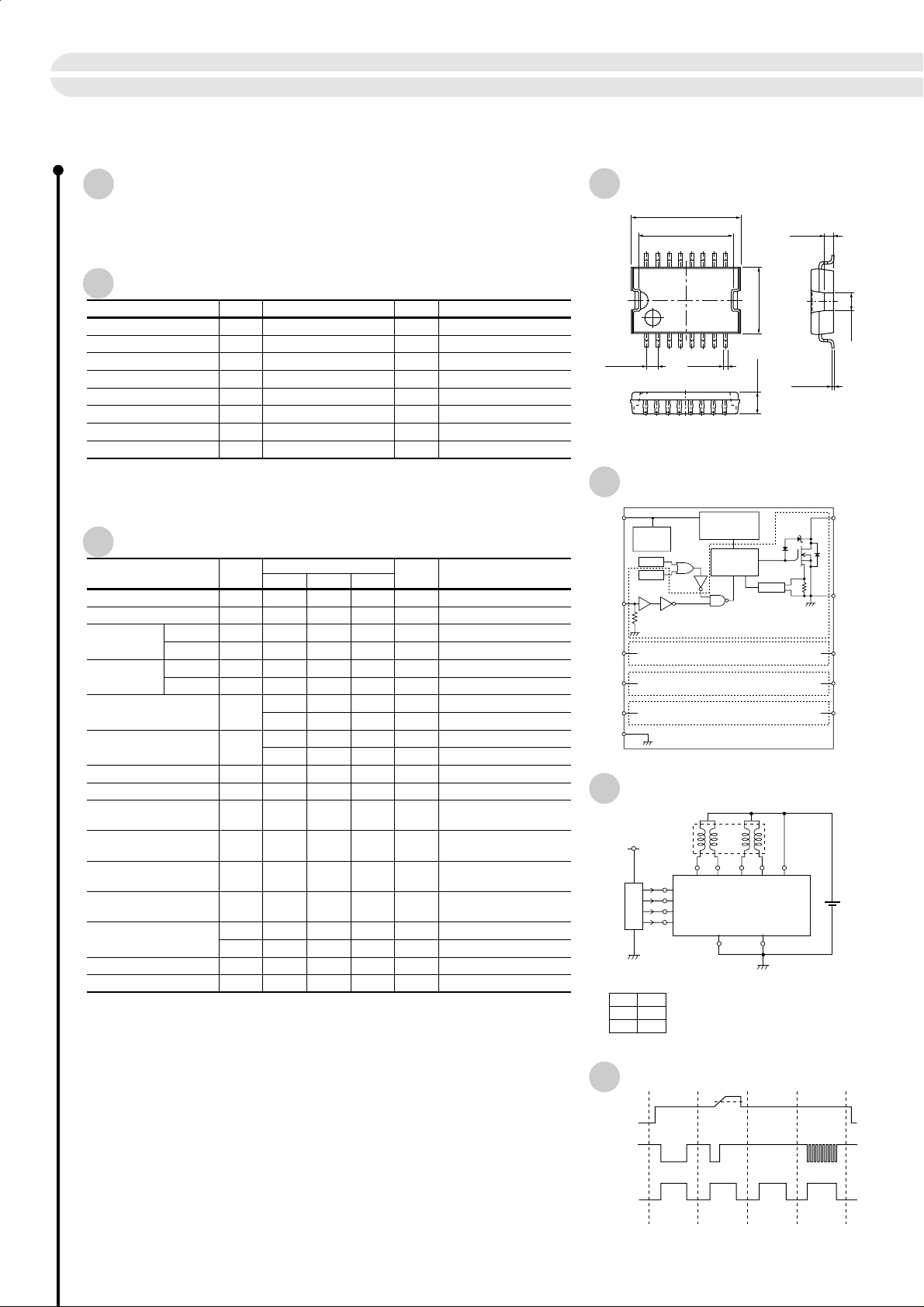
External Dimensions
±0.2
12.2
±0.2
10.5
16
(unit: mm)
9
±0.2
7.5
18
±0.25
1.27
+0.15
–0.05
0.4
±0.2
2.5
Equivalent Circuit Diagram
V
V
V
V
V
L-GND
B
Reg. REF
OVP
TSD
1
IN
250kΩ typ
2
IN
3
IN
4
IN
Gate Protction
Gate Driver
OCP
Circuit Example
Stepper motor
V
CC
CONTROL
UNIT
Truth table
VINV
O
HL
LH
2
OUT1 OUT3 OUT2 OUT4
4
IN1
6
IN2
12
14
SPF5001
IN3
IN4
L-GND P-GND
13
Use L-GND and P-GND being connected.
10 7
15
1,9
1.0
Fin
thickness
0.25
5
V
B
+0.1
–0.05
+0.15
–0.05
+0.2
V
OUT
P-GND
V
OUT
V
OUT
V
OUT
–0.8
2.0
1
2
3
4
38
Timing Chart
OVP
V
B
V
OUT
V
IN
Normal Overvoltage Overheat Overcurrent
* Self-excited frequency is used in the overcurrent protection.
Quiescent Circuit Current
■
10
8
6
Iq (mA)
4
2
Ta = 125ºC
Ta = 25ºC
Ta = –40ºC
Circuit Current (single circuit)
■
12
10
8
= 125ºC
Ta
6
Iq (mA)
4
2
Ta
Ta
= 25ºC
= –40ºC
Circuit Current (4 circuits)
■
V
= 5 V
IN
12
10
8
6
Ta
Ta
Ta
= 125ºC
= 25ºC
= –40ºC
V
= 5 V
IN
Iq (mA)
4
2
0
010203040
VB (V)
Threshold Input Voltage
■
15
Ta = –40ºC
10
(V)
O
V
5
0
01 23
Overvoltage Protection Starting Voltage
■
15
10
(V)
O
V
5
Ta = 25ºC
Ta = 125ºC
V
IN (th)
VO = 14V
= 0.1A
I
O
Ta = –40ºC
Ta = 25ºC
Ta = 125ºC
(V)
VB = 14V
= 14V
V
O
= 0.1A
I
O
0
010203040
VB (V)
Output ON Voltage
■
1.0
0.8
0.6
(V)
DS (ON)
0.4
V
0.2
0
0 0.5 1.0 1.5 2.0
Ta = 125ºC
Ta
= 25ºC
V
V
= 5.5V
B
= 14V
B
Ta = –40ºC
IO (A)
0
010203040
VB (V)
Forward Voltage of Output Stage Diode
■
2.0
Ta = 125ºC
= 25ºC
Ta
= –40ºC
Ta
0 0.5 1.0 1.5
(A)
F
I
1.5
1.0
0.5
0
VF (V)
0
010203040
VB (V)
39
 Loading...