

Sanken Electric Co SMA5113 Datasheet
MOS FET Array SMA5113
Absolute Maximum Ratings
(Ta=25ºC)
Symbol Ratings Unit
V
DSS
V
GSS
I
D
1
I
*
D (pulse)
P
T
2
E
*
AS
I
AS
j-a
j-c
T
ch
Tstg
*
1 P
100µs, duty 1%
W
*
2 V
30V, L
=
DD
50Ω
R
=
G
—
■
I
V
D
7
6
5
4
(A)
D
3
I
2
1
0
0 5 10 15 20
450
±30
±7
±28
4 (Ta=25ºC, All circuits operate, No Fin)
35 (Tc=25ºC, All circuits operate,
130
W
∞
Fin)
W
mJ
7
Junction - Ambientare,
31.2
Ta=25ºC, All circuits operate
Junction - Case,
3.57
Ta=25ºC, All circuits operate
150
–55 to +150
5mH, I
=
Characteristics
DS
10V
ºC/W
ºC/W
7A, unclamped,
=
L
V
(V)
DS
ºC
ºC
Electrical Characteristics
V
V
A
A
A
V
Symbol Test Conditions
V
(BR) DSSID
I
GSS
I
DSS
V
TH
R
e (
yfs)
R
DS (ON
)
Ciss
Coss
Crss
t
on
d
(
)
r
t
off
td
(
)
tf
V
SD
5.5V
5V
= 4.5V
GS
V
DS
V
DS
V
DS
V
GS
I
SD
■
Ratings
min typ max
100µA, V
=
V
GS
450V, V
=
10V, I
=
20V, I
=
10V, I
=
V
f
=
V
I
V
DD
R
V
R
7A, V
=
I
D
(A)
D
I
0V
=
GS
30V
= ±
GS
=
D
=
D
=
D
10V
=
DS
1.0MHz
0V
=
GS
3.5A
=
D
200V
57Ω
=
L
10V
=
GS
50Ω
=
G
=
GS
—
Characteristics
V
GS
7
6
5
4
3
2
1
0
0246810
450
±100
0V
=
1mA 4.0
3.5A 3.5
3.5A
2.0
5.0
0.84 1.1
720
150
65
25
40
70
50
V
GS
1.0 1.5
T
(V)
= –55ºC
a
150ºC
0V
V
= 20V
DS
100
25ºC
(Ta=25ºC)
Unit
V
nA
µA
V
S
Ω
pF
pF
pF
ns
ns
ns
ns
V
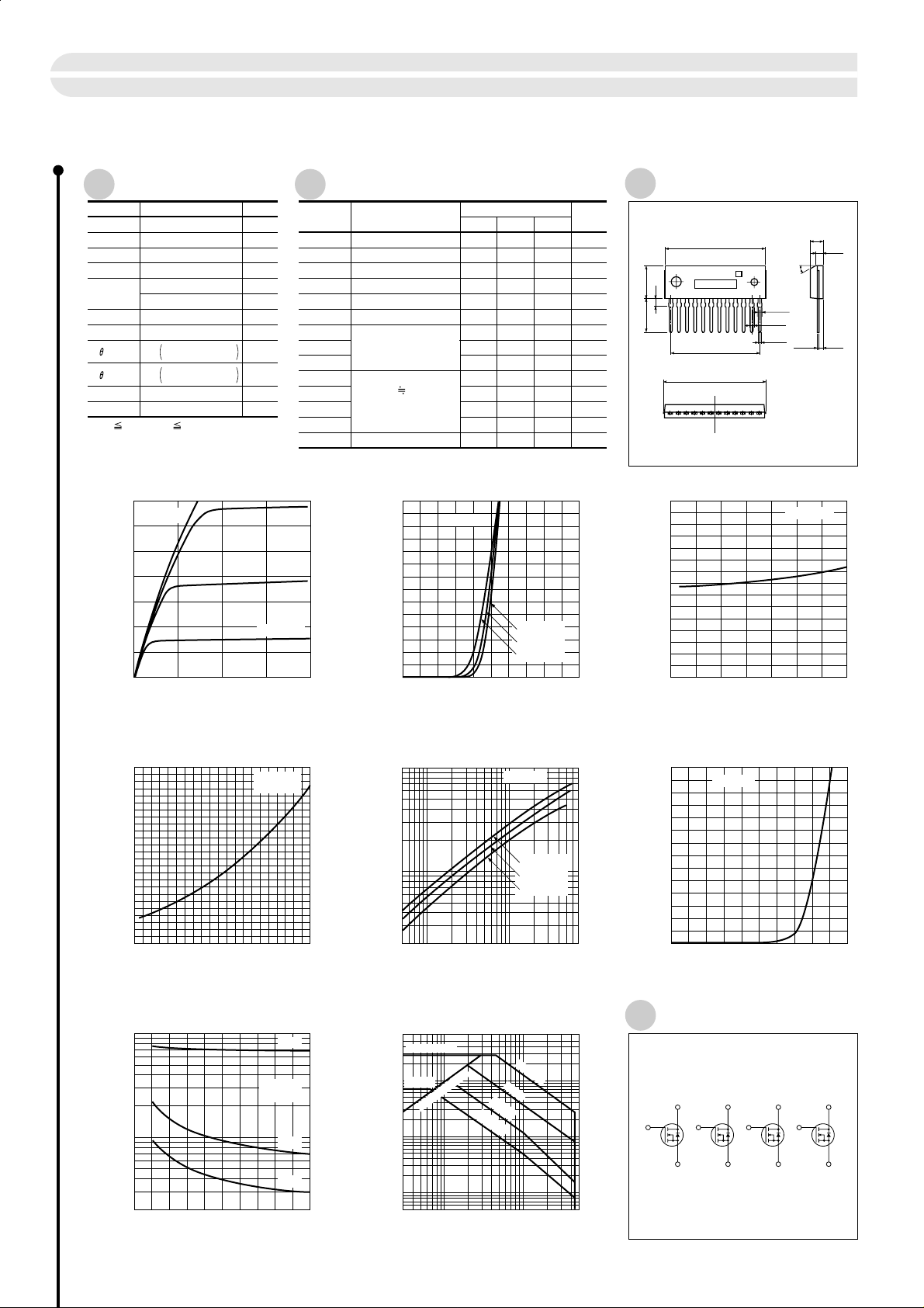
External Dimensions
31.0
±0.2
a
10.2
2.4
(10.4)
11•P2.54
31.5max
123456789101112
■
—
R
(on)
DS
1.5
1.0
(Ω)
DS (on)
R
0.5
I
D
0
01234567
SMA (LF1000)
±0.2
b
1.21
±0.15
1.46
=27.94
0.85
I
(A)
D
±0.1
Characteristics
±0.15
+0.2
–0.1
±0.2
4.0
30º
+0.2
–0.1
0.55
a) Type No.
b) Lot No.
(Unit: mm)
V
= 10V
GS
±0.2
2.5
±0.1
1.2
—
■
R
(on)
DS
2.5
2.0
1.5
(Ω)
DS (on)
1.0
R
0.5
0
–50 0 50 100 150
Characteristics
T
C
V
Tc (ºC)
Capacitance — V
■
1000
500
100
Capacitance (pF)
50
20
01020304050
Characteristics
DS
V
(V)
DS
= 10V
GS
I
= 3.5A
D
V
= 0V
GS
f
= 1MHz
Ciss
Coss
Crss
R
e (yfs)
100
50
—
I
D
V
DS
■
Characteristics
(S)
(yfs)
e
10
R
5
2
0.05 0.1 0.5 1 7
I
(A)
D
Safe Operating Area (single pulse)
■
50
I
max
D
(pulse)
D
max
R
E
IT
IM
L
(on)
DS
10ms
100ms
V
DS
1ms
(V)
10
I
D (DC)
5
(A)
D
I
1
0.5
0.1
0.05
3 5 10 50 100 500
= 20V
T
a
100µs
= –55ºC
25ºC
150ºC
(Ta
= 25ºC)
—
■
(A)
I
I
DR
DR
Characteristics
V
SD
7
6
5
4
3
2
1
0
00.40.2 0.6 0.8 1.0
V
= 0V
GS
V
(V)
SD
Equivalent Circuit Diagram
3
1
2
6
4
5
7
8
9
10
11
12
81
 Loading...