

Sanken Electric Co SLA5008 Datasheet
I
D
(A)
VGS (V)
0 ---2 ---1 0--- 4 ---6 ---8
--- 6
--- 0
--- 1
--- 3
--- 5
--- 4
--- 2
(VDS=–10V)
25°C
125°C
T
C
=–40°C
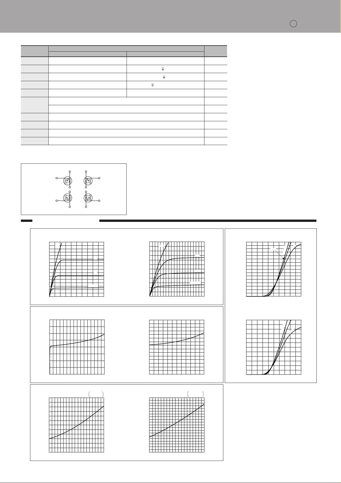
N-channel + P-channel
Ratings
H-bridge
External dimensions
(Ta=25°C)
SLA5008
Absolute maximum ratings
Symbol Unit
N channel P channel
VDSS 100 –100 V
VGSS ±20 20 V
ID ±4 3A
ID(pulse) ±8 (PW≤1ms) 6 (PW≤1ms) A
EAS*15 —mJ
PT
θ
j-c 3.57 °C/W
5 (Ta=25°C, with all circuits operating, without heatsink) W
35 (Tc=25°C,with all circuits operating, with infinite heatsink) W
VISO 1000 (Between fin and lead pin, AC) Vrms
Tch 150 °C
Tstg –40 to +150 °C
* : VDD=20V, L=1mH, ID=5A, unclamped, see Fig. E on page 15.
■Equivalent circuit diagram
Pch
Nch
10
12
11
2
1
7
8
9
4
5
6
3
A
• • •
SLA
Characteristic curves
42
8
7
6
5
(A)
4
D
I
3
2
1
0
020
0.8
0.6
0.4
RDS (ON) (Ω)
0.2
0012 8
1.2
1.0
0.8
(Ω)
0.6
DS (ON)
0.4
R
0.2
--- 4000 50 100
N-ch P-ch N-ch
10V
7V
6V
VGS=5V
10
V
DS
(V)
DS(ON)-ID Characteristics (Typical)
N-ch P-ch P-ch
3456 7
ID (A)
N-ch P-ch
TC (°C)
R
(VGS=10V)
RDS(ON)-TC Characteristics (Typical)
I
D
=
4A
V
GS
=
10V
150
ID-VDS Characteristics (Typical) ID-VGS Characteristics (Typical)
--- 6
–10V
--- 5
--- 4
--- 3
(A)
D
I
--- 2
--- 1
--- 0
0 ---5 ---2 0
1.5
1.0
(Ω)
DS (ON)
R
0.5
0
0
2.0
1.5
(Ω)
1.0
DS (ON)
R
0.5
–4000 50 100
---10 ---15
VDS (V)
–2
–3 –4 –6
ID (A)
TC (°C)
–7V
–6V
GS
=–5V
V
(VGS=–10V)
–5–1
ID=–3A
V
GS
=–10V
25°C
(VDS=10V)
=–40°C
C
T
8
125°C
8
7
6
5
4
(A)
D
I
3
2
1
0
024 6 10
150
VGS (V)
SLA5008
0.5
0.1
1 5 10 50 100
1
5
10
I
D
(A)
VDS (V)
0.5
(TC=25°C)
ID (pulse) max
1ms
10ms (1shot)
R
DS (ON)
LIMITED
100µs
---0.5
---0.1
---1 ---5 ---10 ---50 ---100
--- 1
--- 5
---10
ID (A)
VDS (V)
---0.5
(TC=25°C)
ID (pulse) max
1ms
10ms (1shot)
R
DS (ON)
LIMITED
100µs
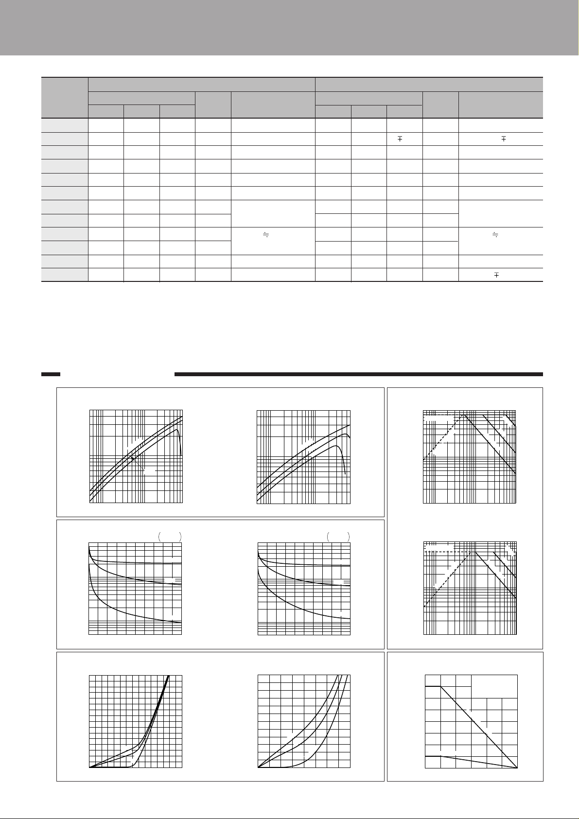
Electrical characteristics
N channel P channel
Symbol Specifications
min typ max min typ max
Unit Conditions
V(BR)DSS 100 V ID=250µA, VGS=0V –100 V ID=–250µA, VGS=0V
IGSS ±500 nA VGS=±20V 500 nA VGS= 20V
IDSS 250
µ
AVDS=100V, VGS=0V –250
VTH 2.0 4.0 V VDS=10V, ID=250µA –2.0 –4.0 V
Re(yfs) 1.1 1.7 S VDS=10V, ID=4A 0.7 1.1 S VDS=–10V, ID=–3A
RDS(ON) 0.50 0.60 Ω VGS=10V, ID=4A 1.1 1.3 Ω VGS=–10V, ID=–3A
Ciss 180 pF VDS=25V, f=1.0MHz, 180 pF
Coss 82 pF VGS=0V 85 pF VGS=0V
ton 40 ns
toff 40 ns
ID=4A, VDD50V, VGS=–10V,
see Fig. 3 on page 16.
VSD 1.2 2.0 V ISD=4A –4.0 –5.5 V ISD=–3A
trr 250 ns ISD=±100mA 250 ns ISD= 100mA
Specifications
90 ns
80 ns
Unit Conditions
µ
AVDS=–100V, VGS=0V
VDS=–10V, ID=–250µA
VDS=–25V, f=1.0MHz,
ID=–3A, VDD–50V, VGS=–10V,
see Fig. 4 on page 16.
(Ta=25°C)
Characteristic curves
5
1
Re (yfs) (S)
0.5
0.2
0.1
0.05 0.5 1
600
100
50
Capacitance (pF)
10
5
01020304050
8
7
6
5
(A)
4
DR
I
3
2
1
0
0 1.0 1.5
N-ch P-ch N-ch
T
=–40°C
C
ID (A)
125°C
25°C
(VDS=10V)
58
5
1
Re (yfs) (S)
0.5
0.2
(VDS=–10V)
=–40°C
C
T
25°C
125°C
–0.1–0.05
–0.5 –1
ID (A)
–6
Capacitance-VDS Characteristics (Typical)
Re(yfs)-ID Characteristics (Typical) Safe Operating Area (SOA)
N-ch P-ch P-ch
VGS=0V
f=1MHz
Ciss
Coss
700
500
100
50
Capacitance (pF)
Crss
VDS (V)
10
5
0 ---10 ---20 ---30 ---40 ---50
VDS (V)
VGS=0V
f=1MHz
Ciss
Coss
Crss
IDR-VSD Characteristics (Typical) PT-Ta Characteristics
N-ch P-ch
10V
5V
=0V
GS
V
0.5
VSD (V)
--- 6
--- 5
--- 4
(A)
--- 3
DR
I
--- 2
--- 1
--- 0
0---3
--- 1
–10V
–5V
=0V
GS
V
--- 2 --- 4
VSD (V)
40
35
30
25
20
(W)
T
P
15
10
Without Heatsink
5
0
0 50 100 150
With Silicone Grease
Natural Cooling
All Circuits Operating
With Infinite Heatsink
Ta (°C)
43
 Loading...