Sanken Electric Co SLA4708M Datasheet

Stepper Motor Driver SLA4708M
Features
● High output breakdown voltage of 50V
● Affluent output current of 1.5A
● Built-in overcurrent, overvoltage and thermal protection circuits
● Low standby current of 50µA
Absolute Maximum Ratings
Parameter Symbol Unit ConditionsRatings
Power supply voltage
Breakdown voltage
Input voltage
Output current
Diagnostic output sink current
Diagnostic output withstand voltage
Operating temperature
Storage temperature
Power Dissipation
V
I
O, AVE
I
DIAG
I
DIAG. H
Top
Tstg
P
V
S
V
O
IN
35
50
–0.3 to +7
10
7
–40 to +85
–40 to +150
D
3.5 (Ta=25ºC)
V
V
V
A1.5
mA
V
ºC
ºC
W
Without heatsink
Electrical Characteristics
Parameter Symbol
Input voltage
(I
, I
standby)
A/A
B/B
Input current
Output saturation voltage
Output leak current
Overcurrent detection
Overvoltage detection
Saturation voltage of diagnostic
output
Standby current
V
I
IL
IH
O.STA
O.STA
O.LEAK
SD
SD
DIAG.L
STB
IL
IH
Ratings
min typ max
2.4
1.8
27.5
50
Unit Conditions
0.8
V
VV
–0.8 mA
50
µAI
1.3 VV
1.5
100
VV
µAI
AI
VV
0.3
VV
µAI
V
IN
V
IN
I
O
IO = 1.5A, Ta = 2 5 º C
V
O
I
DIAG
V
S
(VS=12V, Ta=25ºC)
= 0.4V
= 2.4V
= 1A, Ta = 2 5 º C
= 16V
= 5mA
= 12V
(Ta=25ºC)
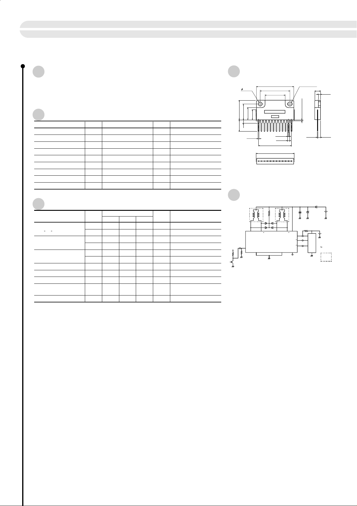
External Dimensions
a
b
11•P2.54
12 3
4 5 6 7 8 9 10 11 12
31.0
24.4
16.4
31.5max
3.2
±0.2
±0.2
16.0
13.0
2.7
9.5min (10.4)
±0.15
±0.2
9.9
8.5max
Pin 1
±0.15
1.2
(unit: mm)
±0.2
±0.2
±0.2
0.85
1.45
±0.7
=
27.94
Ellipse 3.2
12
+0.2
–0.1
±0.15
±1.0
Standard Circuit Diagram
45
OUTAOUT
STBY
5V
2
P-GND
611
4.7kΩ
981
OUT
A
SLA4708M
OUTBV
B
DIAG
L-GND L-GND
N.C.
S
I
A/A
I
B/B
7
±0.15
• 3. 8
0.8max
Lead plate thickness
resins
+0.2
–0.1
0.55
a) Type No.
b) Lot No.
+
ZD
C
12
3
CPU
10
±0.2
4.8
ZD: VS <35V
C 100µF
(Reference)
±0.7
1.7
±0.7
2.2
Stepper
motor
42

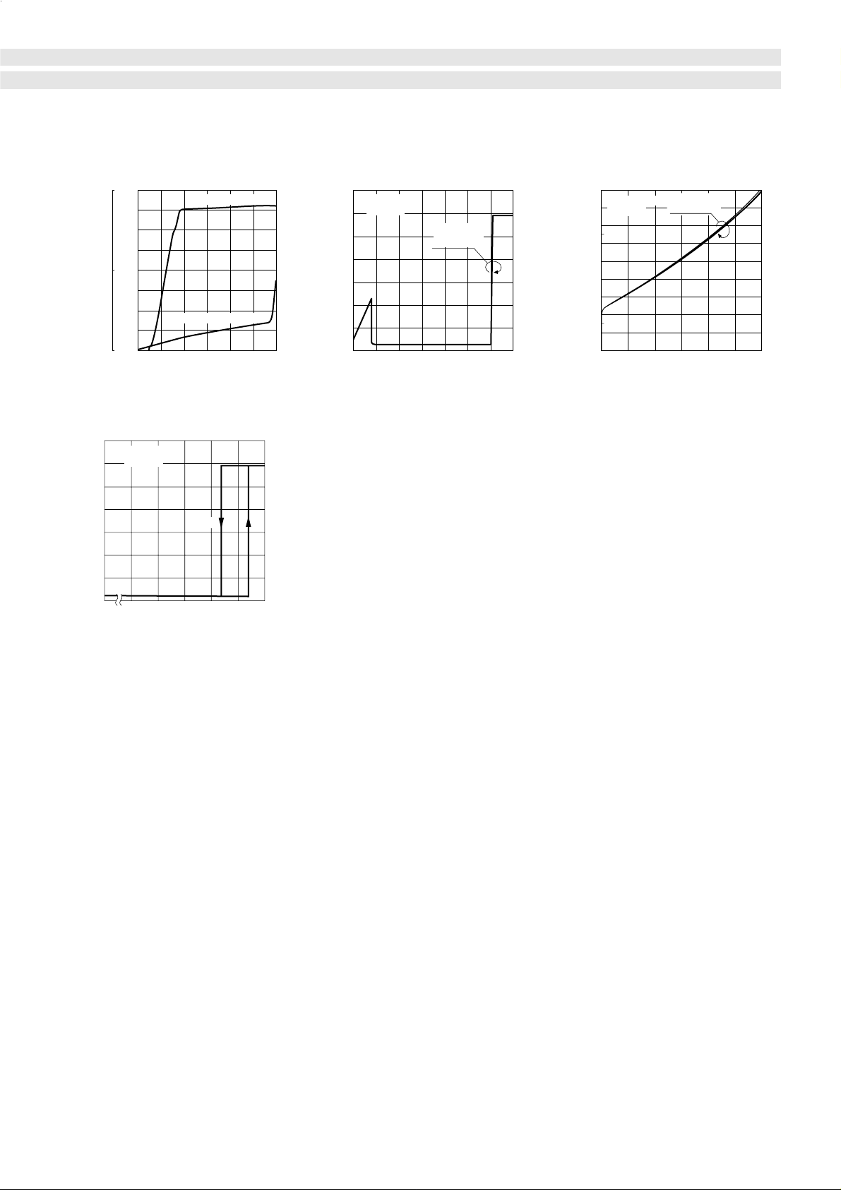
Power Supply Current Characteristics
■
20
200
S (mA)
100
10
At standby IS (µA)
Power supply current
Thermal Protection Characteristics
■
Output voltage VO (V)
At Constant I
0
0
0
Power supply voltage VS (V)
14
Vcc(Vs) =12V
=
V 5V
ST
12
10
8
6
4
2
0
0
110 120 130 140 150 160
Junction temperature Tj (ºC)
Constant (ST = 5V)
At standby (ST = 0V)
10 20 30
T
j2
Overvoltage Protection Characteristics
■
14
=
T 25ºC
a
=
V 12V
cc
12
10
8
6
4
Output voltage VO (V)
2
0
0102030
Power supply voltage VS (V)
T
j1
Common for
all phases
35
Saturation Voltage of Output Transistor Characteristics
■
2.0
Vcc(Vs) =16V
Ta =25ºC
1.5
1.0
0.5
Saturation voltage of output transistor Vsat (V)
0
0 1.0 2.0 3.0
Common for
all phases
Output current IO (A)
43
 Loading...