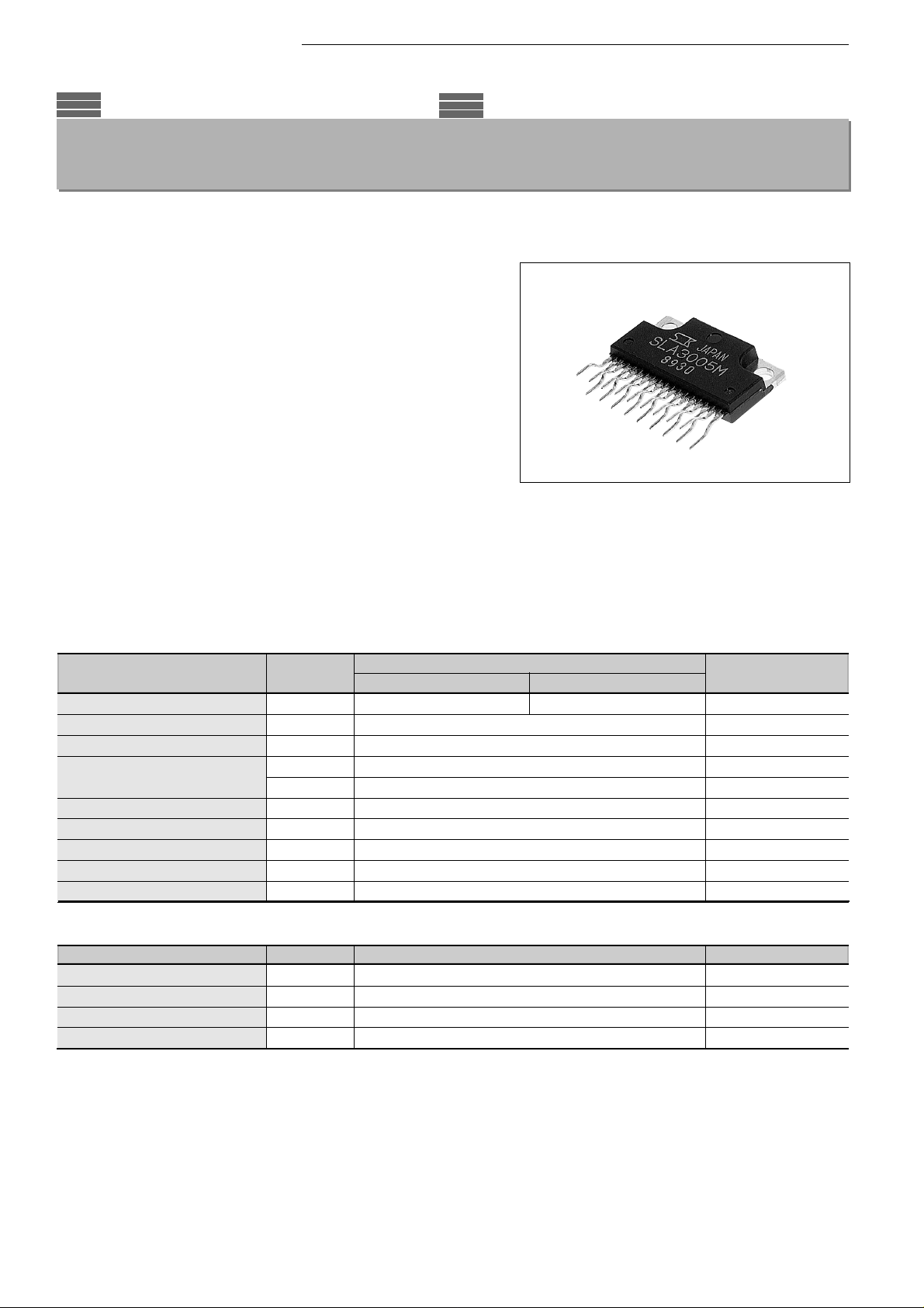
Sanken Electric Co SLA3005M, SLA3006M, SLA3007M Datasheet

●SLA3005M/3006M/3007M
SLA3005M/3006M/3007M
4-Output, Low Dropout Voltage Dropper Type for USB Hub
■Features
• 4 regulators combined in one package
• Insulated single inline package
• SLA3005M/3006M with 5V/0.5A × 4 outputs and SLA3007M with 5V/0.5A × 3,
3.3V/0.5A × 1 outputs
• Low dropout voltage: VDIF≤0.5V (at IO=0.5A)
• Output-independent ON/OFF control terminal compatible with LS-TTL (Active
High)
• Output-independent overcurrent and thermal protection circuits built in
• Open collector flag-output terminals built in to output OCP operation to each
output terminal (Active Low)
• SLA3005M/3007M (excluding Reg4) for VO shutdown aft πer OCP operation and
SLA3006M for continuous OCP operation
• Built-in anti-malfunction delay circuit whose time can be set with an external
capacitor
■Applications
• USB hub power supplies
• Electronic equipment
■Absolute Maximum Ratings
Parameter
DC Input Voltage
Voltage of Output Control Terminal
DC Output Current
Power Dissipation
Junction Temperature
Ambient Operating Temperature
Storage T emperature
Thermal Resistance (junction-to-case)
Thermal Resistance (junction-to-ambient air)
Symbol
VIN
VC
IO
PD1
PD2
Tj
TOP
Tstg
Rt(j-c)
Rth(j-a)
■Recommended Operating Conditions
Parameter
DC Input Voltage Range
Output Current Range
Operating Junction Temperature Range
Ambient Operating Temperature Range
Symbol
VIN
IO
Tjop
Taop
Ratings
SLA3005M/3006M SLA3007M
20 18
VIN
0.5
30(With infinite heatsink)
3.36(Without heatsink, stand-alone operation)
–30 to +125
–30 to +100
–30 to +125
9.0
29.8(Without heatsink, stand-alone operation)5V/0.5A × 4
Ratings
5.5 to 10
0 to 0.5
–20 to +100
–20 to +85
(Ta=25°C)
Unit
V
V
A
W
W
°C
°C
°C
°C/W
°C/W
Unit
V
A
°C
°C

●SLA3005M/3006M/3007M
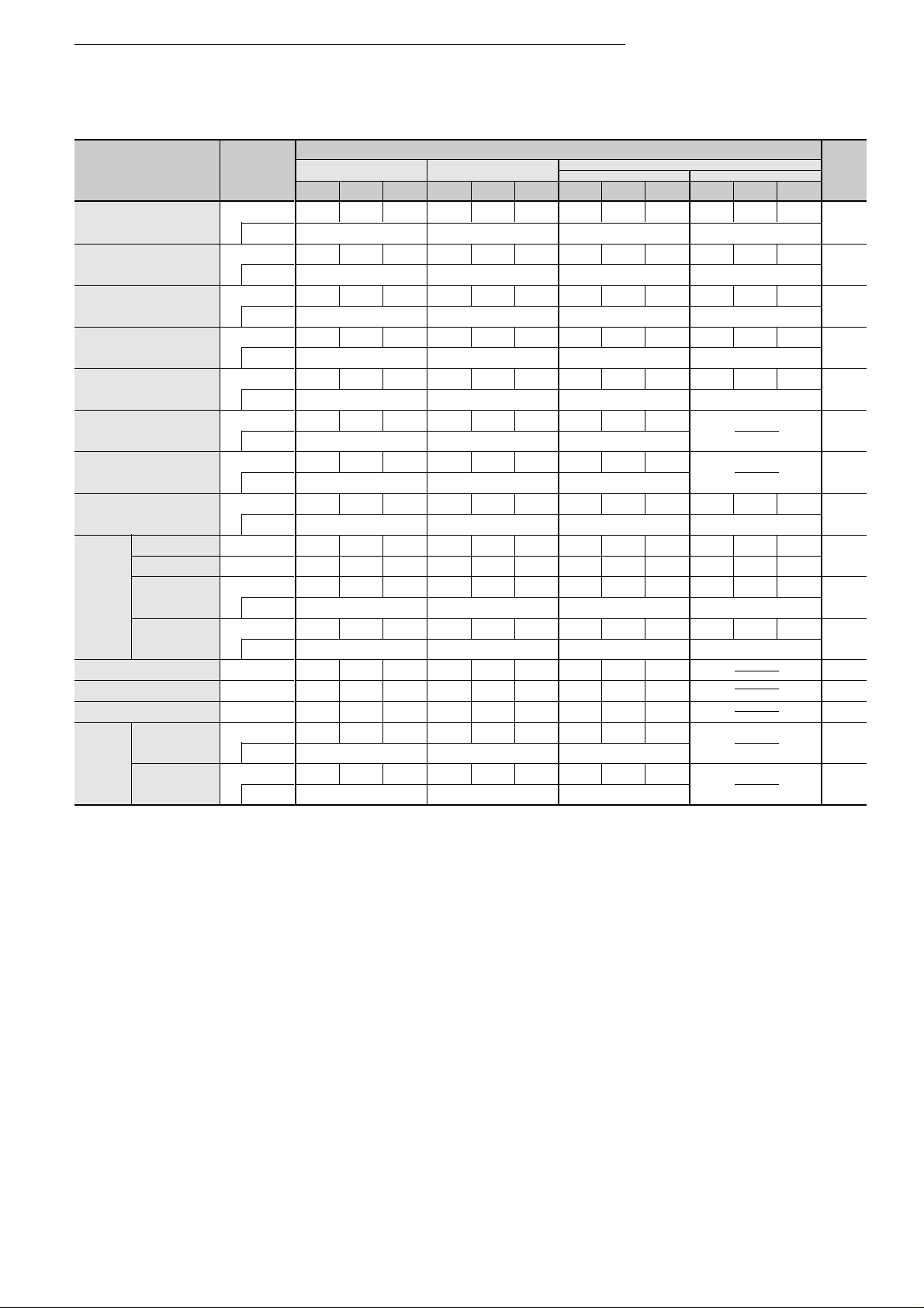
■Electrical Characteristics
Parameter
Output Voltage
Dropout Voltage
Line Regulation
Load Regulation
Temperature Coefficient
of Output Voltage
Quiescent Circuit
3
Current*
Quiescent Circuit
Current (Output OFF)*
Overcurrent Protection
Starting Current*
1
Control Voltage (Output ON)
Control Voltage (Output OFF)
VC
Control Current
Terminal*2(Output ON)
Control Current
(Output OFF)
OCP Detection Voltage Level
Delay Threshold V oltage
Delay Terminal Runoff Current
Flag
Output
Terminal
Before OCP
Detection
After OCP
Detection
3
SYmbol
VO
Conditions
VDIF
Conditions
∆VOLINE
Conditions
∆VOLOAD
Conditions
∆VO/∆Ta
Conditions
Iq
Conditions
Iq(off)
Conditions
IS1
Conditions
VC. IH
VC. IL
IC. IH
Conditions
IC. IL
Conditions
Voth
VDLYth
IDLY
VFLGh
Conditions
VFLGl
Conditions
SLA3005M
min. typ. max.
4.85 5.00 5.15
VIN=7V, IO=0.1A
0.5
IO≤0.5A
30
VIN=6 to 15V, IO=0.1A
50
VIN=7V, IO=0 to 0.5A
±0.5
VIN=7V, IO=5mA, Tj=–10 to 100°C
20
VIN=7V, IO=0A
0.5
VIN=7V , V C1 to 4=0V
0.55 0.65
VIN=7V
2.0
0.7
50
VC=2.7V
–100
VC=0V
3.7 4.0 4.3
2.1 2.3 2.5
35 50 65
VIN–0.4
R
FLG
connected between FLG and V
0.5
IFLG=1mA
SLA3006M
min. typ. max.
4.85 5.00 5.15
VIN=7V, IO=0.1A
IO≤0.5A
VIN=6 to 15V, IO=0.1A
VIN=7V, IO=0 to 0.5A
±0.5
VIN=7V, IO=5mA, Tj=–10 to 100°C
VIN=7V, IO=0A
VIN=7V , VC 1 to 4=0V
0.75 0.96
VIN=7V
2.0
VC=2.7V
VC=0V
3.7 4.0 4.3
2.1 2.3 2.5
35 50 65
VIN–0.4
IN
R
FLG
connected between FLG and V
IFLG=1mA
Ratings
Regulator1, 2, 3 Regulator4
min. typ. max.
4.85 5.00 5.15
VIN=7V, IO=0.1A
0.5
30
VIN=6 to 15V, IO=0.1A
50
VIN=7V, IO=0 to 0.5A
VIN=7V, IO=5mA, Tj=–10 to 100°C
20
VIN=7V, IO=0A
0.5
VIN=7V , V C1 to 4=0V
0.55 0.65
2.0
0.7
50
–100
3.7 4.0 4.3
2.1 2.3 2.5
35 50 65
VIN–0.4
IN
R
FLG
connected between FLG and V
0.5
IO≤0.5A
±0.5
VIN=7V
VC=2.7V
VC=0V
IFLG=1mA
(Ta=25°C unless otherwise specified)
SLA3007M
min. typ. max.
3.234 3.300 3.366
VIN=7V, IO=0.1A
0.5
IO≤0.5A
30
VIN=6 to 15V, IO=0.1A
50
VIN=7V, IO=0 to 0.2A
±0.3
VIN=7V, IO=5mA, Tj=–10 to 100°C
20
0.5
0.55 0.65
VIN=7V
2.0
0.7
50
VC=2.7V
–100
–100
VC=0V
IN
0.5
2.0
30
30
0.7
50
Unit
V
V
mV
mV
mV/°C
mA
mA
A
V
µA
µA
V
V
µA
V
V
*1 IS1 is specified at –5(%) drop point of output voltage VO on the condition that VIN = 7V, IO = 0.1A.
*2 Output is ON even when output control terminal VC is open. Each input level is equivalent to LS-TTL. Therefore, it may be directly driven by an
LS-TTL circuit.
*3 Total of four circuits
*4 The FLG output latched by delay DLY after OCP detection. (SLA3005M/3007M(Reg1 to 3) shuts down the output voltage simultaneously at
latching.) Set the VIN or VC to low to reset latching. Leave a time lag of Cd × 600s or more before restart.

●SLA3005M/3006M/3007M
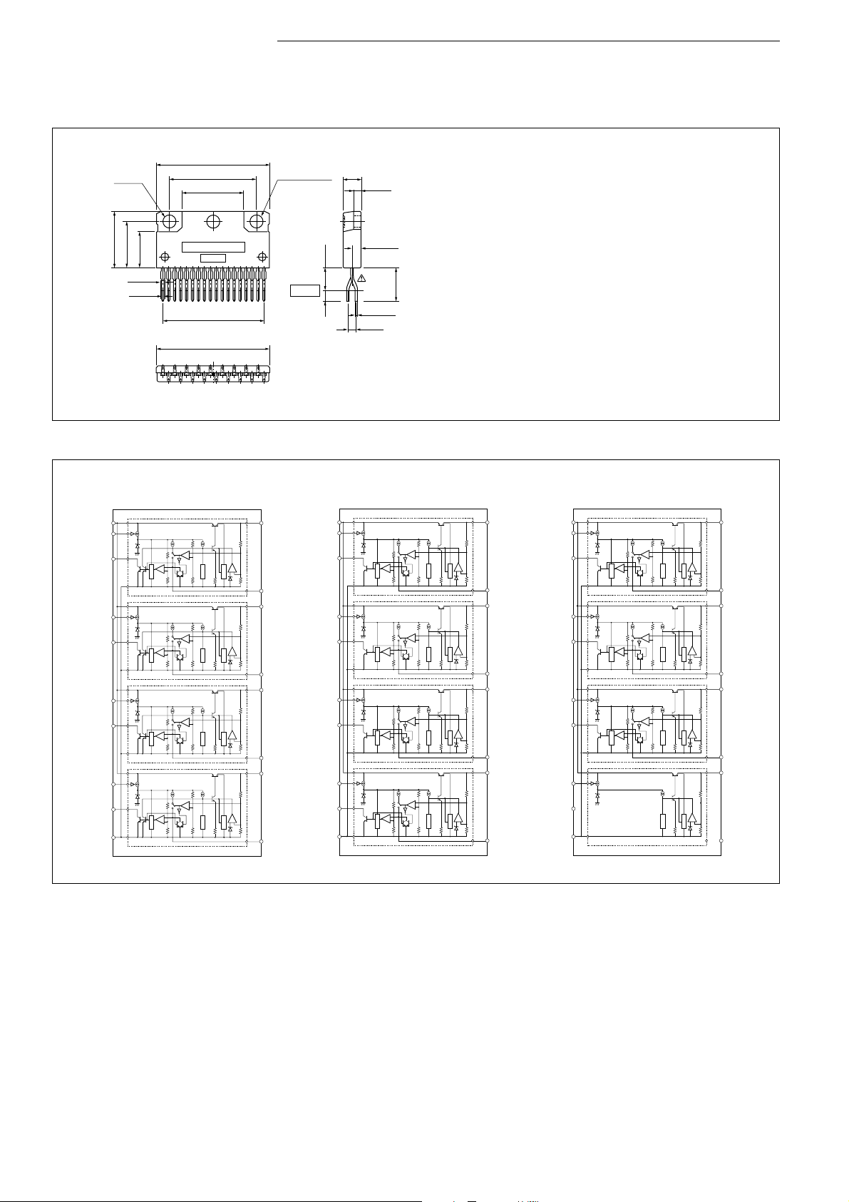
■Outline Drawing
±0.15
3.2
φ
±0.2
±0.2
±0.2
16
13
9.9
+0.2
1
–0.1
+0.2
0.65
–0.1
13579
■Block Diagram
SLA3005M SLA3006M SLA3007M
V
IN
(18pin)
V
C1
(1pin)
FLG
FLG
FLG
(10pin)
(14pin)
FLG
(15pin)
GND
(13pin)
1
(2pin)
V
C2
(5pin)
2
(6pin)
V
C3
(9pin)
3
V
C4
4
Reset
Reset
Reset
Reset
Latch
Set
Latch
Set
Latch
Set
Latch
Set
+
–
+
–
+
–
+
–
SK JAPAN
a
b
*
17×P1.68
–
+
–
+
–
+
–
+
31
24.4
16.4
31.3
8642
TSD
TSD
TSD
TSD
±0.2
±0.7
±0.2
±0.2
*
=28.56
±0.2
11 13 15 17
+
–
OCP
+
–
OCP
+
–
OCP
+
–
OCP
(unit:mm)
× 3.8
±0.5
±0.2
4.8
±0.1
1.7
q VC1
w FLG1
±0.2
2.45
6.7
+1
–0.5
9.7
+0.2
0.55
(3)
–0.1
±0.7
4
*
e DLY1
r VO1
t VC2
y FLG2
u DLY2
i VO2
o VC3
!0 FLG3
!1 DLY
a. Part Number
b. Lot Number
!2 VO3
!3 GND
!4 VC4
!5 FLG4(N. C on SLA3007M)
!6 DLY4(N. C on SLA3007M)
!7 VO4
!8 VIN
Weight:Approx. 6g
V
(18pin)
FLG
FLG
FLG
(10pin)
(14pin)
FLG
(15pin)
GND
(13pin)
V
IN
V
C1
(1pin)
–
Reset
Reset
Reset
Reset
+
+
–
Latch
Set
Latch
Set
Latch
Set
Latch
Set
TSD
–
+
+
–
TSD
–
+
+
–
TSD
–
+
+
–
TSD
1
(2pin)
V
C2
(5pin)
2
(6pin)
V
C3
(9pin)
3
V
C4
4
O1
(4pin)
+
–
OCP
DLY
1
(3pin)
V
O2
(8pin)
+
–
OCP
DLY
2
(7pin)
V
O3
(12pin)
+
–
OCP
DLY
3
(11pin)
V
O4
(17pin)
+
–
OCP
DLY
4
(16pin)
(18pin)
FLG
FLG
FLG
(10pin)
(14pin)
(15pin)
GND
(13pin)
(2pin)
(5pin)
(6pin)
(9pin)
N.C.
V
IN
V
C1
(1pin)
1
V
C2
2
V
C3
3
V
C4
Reset
Reset
Reset
Reg1
–
+
+
–
Latch
Set
Latch
Set
Latch
Set
TSD
Reg2
–
+
+
–
TSD
Reg3
–
+
+
–
TSD
Reg4
TSD
V
O1
(4pin)
+
–
OCP
DLY
1
(3pin)
V
O2
(8pin)
+
–
OCP
DLY
2
(7pin)
V
O3
(12pin)
+
–
OCP
DLY
3
(11pin)
V
O4
(17pin)
+
–
OCP
N.C.
(16pin)
±0.15
3.2
φ
R-END
±1
16141210
18
V
O1
(4pin)
DLY
1
(3pin)
V
O2
(8pin)
DLY
2
(7pin)
V
O3
(12pin)
DLY
3
(11pin)
V
O4
(17pin)
DLY
4
(16pin)
 Loading...