Sanken Electric Co SLA2502M Datasheet

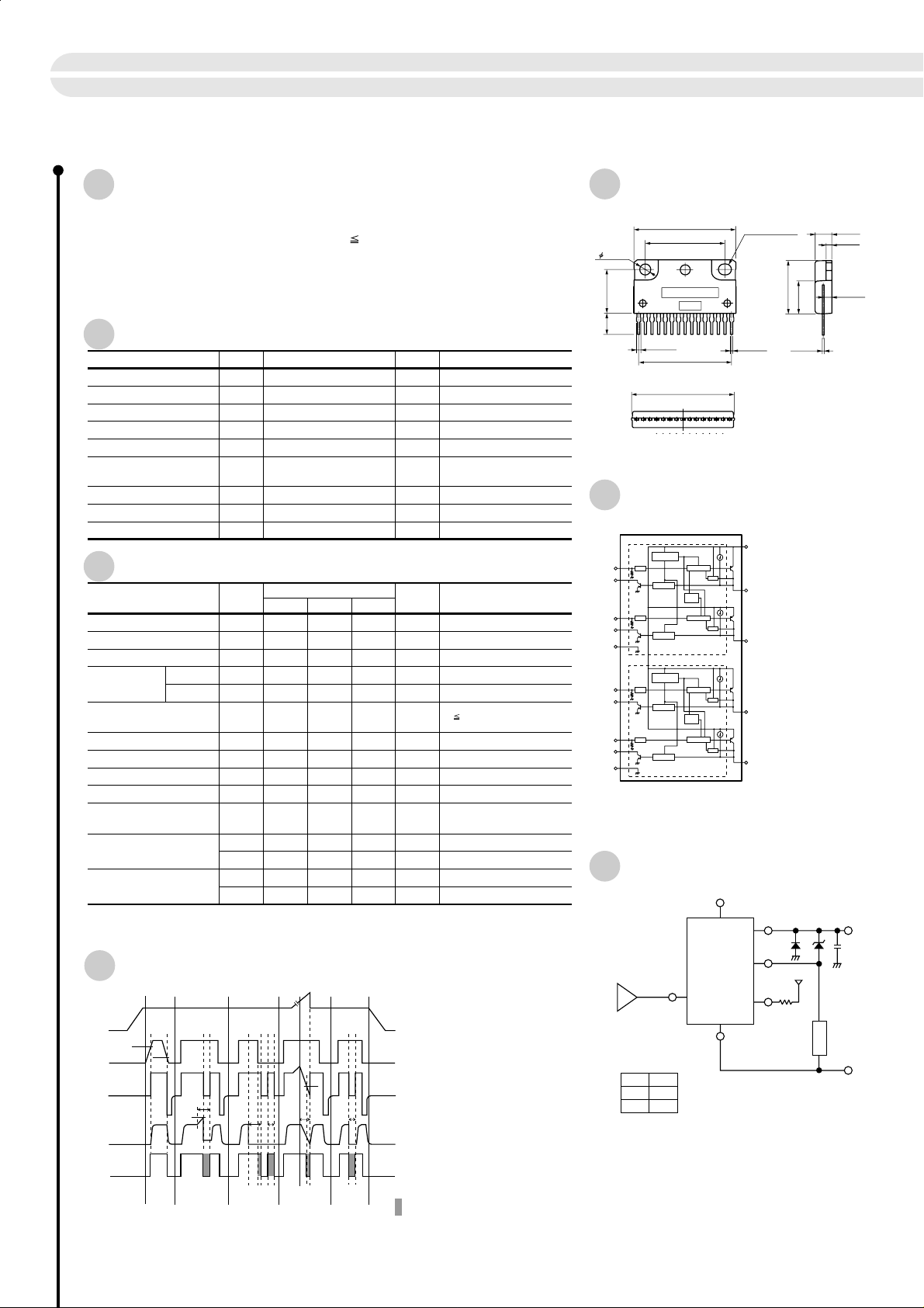
4-circuit High-side Power Switch Array SLA2502M
Features
● Built-in diagnostic function to detect short and open circuiting of loads and
output status signals
● Low saturation PNP transistor use (V
CE (sat)
0.5V)
● Allows direct driving using LS-TTL and C-MOS logic levels
● Built-in overcurrent and thermal protection circuits
● Built-in protection against reverse connection of power supply
● Tj = 150ºC guaranteed
Absolute Maximum Ratings
Parameter Symbol Unit ConditionsRatings
Power supply voltage
Input terminal voltage
DIAG output applied voltage
DIAG output source current I
Output current I
Power Dissipation
Junction temperature
Operating temperature
Storage temperature
V
T
Tstg
V
V
DIAG
DIAG
P
B
IN
O
D
Tj
OP
Electrical Characteristics
Parameter Symbol
V
Operating power supply voltage
Quiescent circuit current (per circuit)
Threshold input voltage
Input current
Hi output
Lo output
Saturation voltage of output
transistor
Output terminal sink current
Saturation voltage of DIAG output
Leak current of DIAG output
Open load detection resistor
Overcurrent protection starting
current
Output transfer time
DIAG output transfer time
Note: * The rule of protection against reverse connection of power supply is VB= –13V, one minute
(all terminals except V
Bopr
Iq
th
IN
I
IN
I
IN
CE (sat)
O (off)
V
DL
DGH
Ropen
S
T
ON
T
OFF
T
PLH
T
PHL
and GND should be open).
B
–13 to +40
–0.3 to +7.0
–0.3 to +7.0
4.8
–40 to +150
–40 to +100
–50 to +150
(V
=14V, Ta=25ºC unless otherwise specified)
Bopr
Ratings
min typ max
6.0
16
512
0.8
3.0 VV
1.0
0
100
30
1.6 AI
8 30
15
30
10
30
15
30
V
V
V
mA3
A1.2
Stand-alone operation without
W
heatsink; all circuits operating
ºC
ºC
ºC
Unit Conditions
V
V
mA
mA
mAI
= 0 V
IN
V
= 5 V
IN
V
= 0 V
µA
IN
VV
1.0A, V
I
O
V
= 0V, V
O
V
I
= 3mA0.3
DIAG
µAI
= 5 V100
V
DIAG
kΩ
V
= V
O
Bopr
µS
I
= 1 A
O
µS
I
= 1 A
O
µS
I
= 1 A
O
µS
I
= 1 A
O
IN
–1.9V
Bopr
= 0 V2.0
(Ta=25ºC)
= 6 to 16V0.5
Diagnostic Function
V
B
GND
3.0V
0.8V
V
IN
GND
V
OUT
GND
GND
I
O
V
DIAG
SHORT
Is
Normal Shorted load Open load Overvoltage Overheat
OVER
VOLTAGE
OPENOPEN
TSD
External Dimensions
±0.2
31
±0.2
±0.15
3.2
±0.2±0.5
12.9
6.4
24.4
a
b
+0.2
–0.1
1.15
±0.1
14 • P2.03 = (28.42)
±0.2
31.3
123 15
(unit: mm)
±0.15
Ellipse 3.2 • 3.8
±0.2
16
+0.2
–0.1
0.65
a: Type No.
b: Lot No.
0.55
±0.2
9.9
+0.2
–0.1
Equivalent Circuit Diagram
SLA2502M
The MIC is bound by the dotted lines.
2
CONT.
NI1
11kΩ typ.
3
DIAG1
6
CONT.
NI2
11kΩ typ.
5
DIAG2
4
GND1
10
CONT.
NI3
11kΩ typ.
11
DIAG3
14
CONT.
NI4
11kΩ typ.
13
DIAG4
12
GND4
[Abbreviations]
Drive: Drive circuit
CONT: ON/OFF circuit
Pre.Reg: Pre-regulator
Pre. Reg.
DIAG DET
T.S.D
DIAG DET
Pre. Reg.
DIAG DET
T.S.D
DIAG DET
8
V
B
Drive
O.C.P
1
Out1
Drive
O.C.P
7
Out2
Drive
O.C.P
9
Out3
Drive
O.C.P
15
Out4
DIAG.DET.: Diagnostic circuit
O.C.P.: Overcurrent protection
T.S.D.: Thermal protection
Standard Circuit Diagram
P
Z
D
1
Out
SLA2502M
IN
Truth table
VINV
O
HH
LL
Note 1: A pull-down resistor (11kΩ typ.) is connected to the IN
terminal.
V
turns "L" when a high impedance is
OUT
connected to the IN terminal in series.
Note 2: Grounds GND1 and GND2 are not wired internally. They
must be shorted at a pattern near the product.
DIAG
5.1kΩ
V
CC
Load
4.8
1.7
2.45
V
GND
±0.2
±0.1
±0.2
B
34
ERROR SIGNAL for CPU

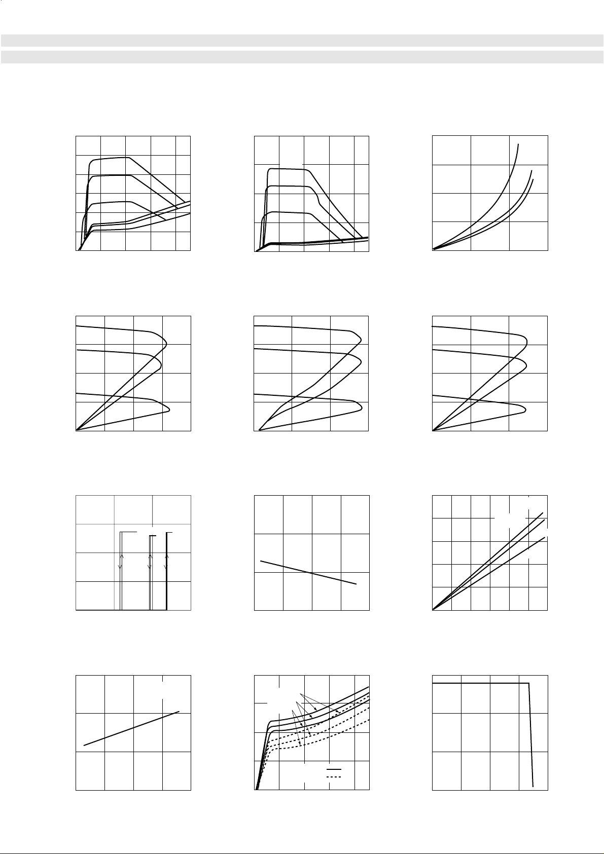
Circuit Current (single circuit)
■
60
50
40
30
(mA)
B
I
20
10
0
0102030
Overcurrent Protection Characteristics (Ta=–40ºC)
■
20
15
(V)
10
O
V
5
Ta
–40ºC
125ºC
V
IN
=
25ºC
= 0 V
V
(V)
B
V
B
18V
14V
Circuit Current (4 circuits)
■
200
150
100
(mA)
B
I
50
4640
=
6V
0
Overcurrent Protection Characteristics (Ta=25ºC)
■
20
15
(V)
10
O
V
5
Ta =
–40ºC
25ºC
125ºC
= 0 V
V
IN
0102030
V
(V)
B
4640 0 1 2
VB =
18V
14V
6V
Saturation Voltage of Output Transistor
■
1.0
I
O
Ta =
125ºC
(A)
(V)
0.5
(sat)
CE
V
0
Overcurrent Protection Characteristics (Ta=125ºC)
■
20
15
(V)
10
O
V
5
(V
V
B
25ºC
V
B
= 14V)
B
–40ºC
=
18V
14V
6V
3
0
012
I
(A)
O
Threshold Input Voltage
■
20
15
(V)
10
O
V
5
0
012
Saturation Voltage of DIAG Output
■
0.3
0.2
(V)
DL
V
0.1
0
–50 0 50 100
Ta =
125ºC
25ºC
V
(V)
IN
VB = 14V
I
Ta (ºC)
DIAG
–40ºC
= 3mA
150
0
43
3
012
I
(A)
O
Input Current (Output OFF)
■
3
2
(µA)
IL
I
1
0
0–50 10050
VB = 14V
= 0 V
V
IN
3
150
Ta (ºC)
Quiescent Circuit Current (dual circuit)
■
20
Ta = –40V
25V
125V
(mA)
10
Iq
VO shorted
V
O
0
0102030
open
V
B
(V)
V
= 0 V
IN
4640
0
012
I
(A)
O
Input Sink Current (Output Hi)
■
0.5
0.4
0.3
(mA)
IH
I
0.2
0.1
0
Thermal Protection Characteristics
■
15
10
(V)
O
V
5
0
210543
500 100 150
Ta
V
(V)
IN
V
B
=
–40ºC
= 14V, IO = 10mA
Ta (ºC)
3
VB = 14V
25ºC
125ºC
6
200
35
 Loading...