Sanken Electric Co SI-3201S Datasheet

Switching Type Regulator SI-3201S
Features
● Output current of 3A (Ta = 25ºC, VIN = 8 to 18V)
● High efficiency of 82% (VIN = 14V, IO = 2A)
● Requires 5 external components only
● Built-in reference oscillator (60kHz)
● Phase internally corrected
● Output voltage internally corrected
● Built-in overcurrent and thermal protection circuits
● Built-in soft start circuit
Absolute Maximum Ratings
Parameter Symbol Unit ConditionsRatings
Input voltage
Output voltage
SQ terminal voltage with respect
to ground
Power Dissipation
Junction temperature
Storage temperature
Junction to case thermal resistance
Junction to ambient-air thermal
resistance
V
Tstg
V
O, SQ
P
P
IN
I
O
D1
D2
Tj
j-c
j-a
35
3
–1
22
1.8
–40 to +150
–40 to +125
5.5
66.7
V
A
V
W
W
ºC
ºC
ºC/W
ºC/W
With infinite heatsink
Stand-alone
(Ta=25ºC)
Recommended Operating Conditions
Parameter Symbol
Input voltage
Output current
Operating temperature
Top
V
IN
I
O
Electrical Characteristics
Parameter Symbol
Output voltage
Line regulation
Load regulation
1
*
Efficiency
Oscillation frequency
Quiescent circuit current
Overcurrent protection starting
current
Low level voltage
3
*
Soft
start
Source current when low
terminal
Discharge resistance
Notes:
*1. Efficiency is calculated by the following equation:
VO • I
O
= • 100 (%)
VIN • I
*2. A drooping-type overcurrent protection circuit is built in the IC.
IN
*3. An external voltage may not be applied to the soft start terminal. As shown in the diagram to the
right, use this IC in the soft start mode with a capacitor or in the open-collector drive mode with a
transistor. Leave the soft start terminal open when not using it since it is already pulled up in the IC.
V
O
O
LINE
V
O
LOAD
OSC
S
V
SSL
I
SSL
R
DIS
Ratings
min typ max
8
0.5
–40
(VIN = 14V, I
18
3
+85
= 2A, Tj = 25ºC unless otherwise specified)
OUT
Ratings
min typ max
4.80 5.00
5.20
100
50 mV
82
50 60
70 kHzf
10 mAIq
5
3.1
0.2
15 µA
25 35
4
Unit Conditions
V
A
Ta—PD characteristicsºC
Unit Conditions
V
V
mV V
= 8 to 18V
IN
= 0.5 to 3A
I
O
%
I
= 0 A
O
2
AI
*
V
V
= 0.2V
SSL
kΩ
±0.2
4.0
±0.2
7.9
±0.3
(4.6)
1. V
2. SW
3. GND
4. V
5. SS
16.9
IN
OS
(unit: mm)
4.2
2.8
2.6
+0.2
–0.1
0.45
±0.7
3.9
(4.3)
±0.7
8.2
OUT
±0.2
±0.2
±0.1
(2.0)
a: Type No.
b: Lot No.
(17.9)
±0.6
5.0
(8.0)
External Dimensions
±0.2
3.2
±0.2
10.0
a
b
P1.7 •4 =6.8
12345
0.5
±0.15
0.95
+0.2
–0.1
0.85
±0.7±0.7
(Forming No. 1101)
Standard Circuit Diagram
L
V
IN
C
1
C
3
GND GND
C1: 1000µF
C2: 1000µF
a: Internal power supply
b: Thermal protection
c: Reference oscillator
d: Reset
e: Latch & driver
Cautions:
(1) A high-ripple current flows through
type
1000µF or higher capacitors with low internal resistance.
Refer to the respective data books for more information on
reliability and electrical characteristics of the capacitor.
(2)
C
is a capacitor used for soft start.
3
(3)
L
should be a choke coil with a low core loss for switching
1
power supplies.
(4) Use a Schottky barrier diode for
reverse voltage applied to the 2nd terminal (SQ terminal) is
within the maximum ratings (–1V). If you use a fast-recovery
diode, the recovery voltage and the ON forward voltage may
cause a reversed-bias voltage exceeding the maximum ratings
to be applied to the 2nd terminal (SQ terminal). Applying a
reversed-bias voltage exceeding the maximum rating to the
2nd terminal (SQ terminal) may damage the IC.
(5) The 4th terminal (
Since this terminal has a high impedance, connect it to the
positive (+) terminal of
(6) Leave the 5th terminal (soft start terminal) open when not
using it. It is pulled up internally.
(7) To ensure optimum operating environment, connect the high-
frequency current line with minimum wiring length.
SI-3201S
V
IN
a
c
SS
5
V
) is an output voltage detection terminal.
S
SW Tr
CQ
b
d
e
f
g
h
i
GND
3
L1: 250µH
D1: RK46 (Sanken)
f: Comparator
g: Overcurrent protection
h: Error amplifier
i : Reference voltage
C
and C2. Use high-ripple
1
D
and make sure that the
1
C
via the shortest possible route.
2
1
21
D
1
4
V
S
V
O
++
C
2
18
SI-3201S SI-3201S SI-3201S
SS5 SS
C
3
5SS5
C
3

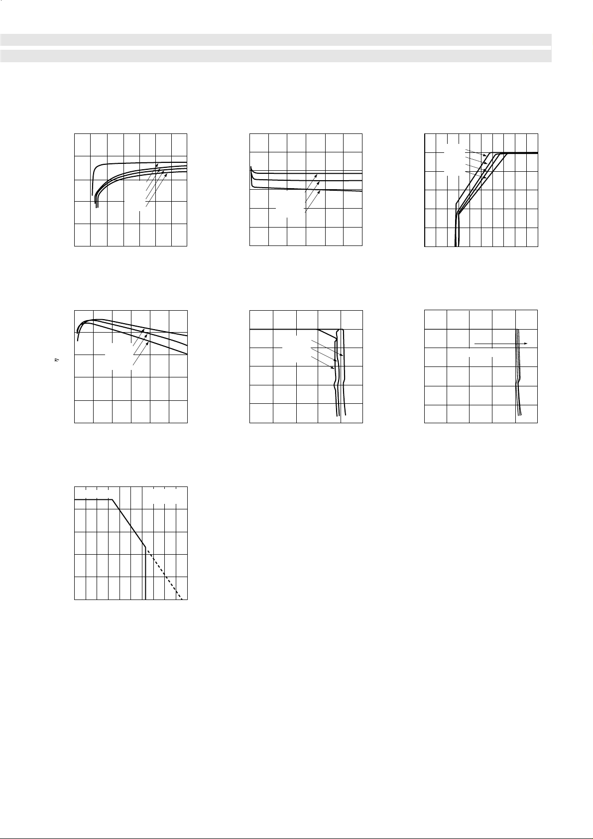
Line Regulation
■
5.10
5.05
5.00
4.95
4.90
Output voltage VO (V)
4.85
0 5 10 15 20 25 30 35
Input voltage V IN (V)
=
I 0A
o
=
1A
=
2A
=
3A
Load Regulation
■
5.15
5.10
5.05
O (V)
5.00
4.95
Output voltage V
4.90
4.85
0
0.5 1.0 1.5 2.0 2.5 3.0
=
V 18V
IN
=
10V
=
7V
Output current I
O (A)
Rise Characteristics
■
6
5
4
O (V)
3
=
=
=
=
I 0A
o
2
1
Output voltage V
0
0
246810
Input voltage V
1A
2A
3A
IN (V)
Efficiency Curve
■
90
80
V 18V
70
IN
60
Efficiency (%)
50
40
0
0.5 1.0 1.5 2.0 2.5 3.0
Output current IO (A)
Ta—PD Characteristics
■
25
With infinite heatsink
20
15
10
5
Power Dissipation PD (W)
=
=
10V
=
7V
With silicone grease
Heatsink: aluminum
Overcurrent Protection Characteristics
■
6
5
=
V 18V
IN
4
O (V)
=
10V
=
7V
3
2
Output voltage V
1
0
0
1.0 2.0 3.0 4.0 5.0
Output current IO (A)
Overcurrent Protection Temperature Characteristics
■
6
5
4
=
+
T 100, 25, 20ºC
C
--
3
2
Output voltage VO (V)
1
0
0 1.0 2.0 3.0 4.0 5.0
Output current IO (A)
0
–40 0 40 80 120 160
Operating temperature Ta (ºC)
19
 Loading...