Sanken Electric Co SI-3102S Datasheet

Dropper Type Dual Output Regulator SI-3102S
16
Features
● Single input dual output <sub output (5V/0.04A), main output (5V/0.1A)>
● Main output can be externally turned ON/OFF (with ignition switch, etc.)
<most suitable as memory backup power supply>
● Low standby current ( 0.8mA)
● Low dropout voltage 1V
●
Built-in constant current type overcurrent, overvoltage and thermal protection circuits
● TO-220 equivalent 5-terminal full-mold miniature package
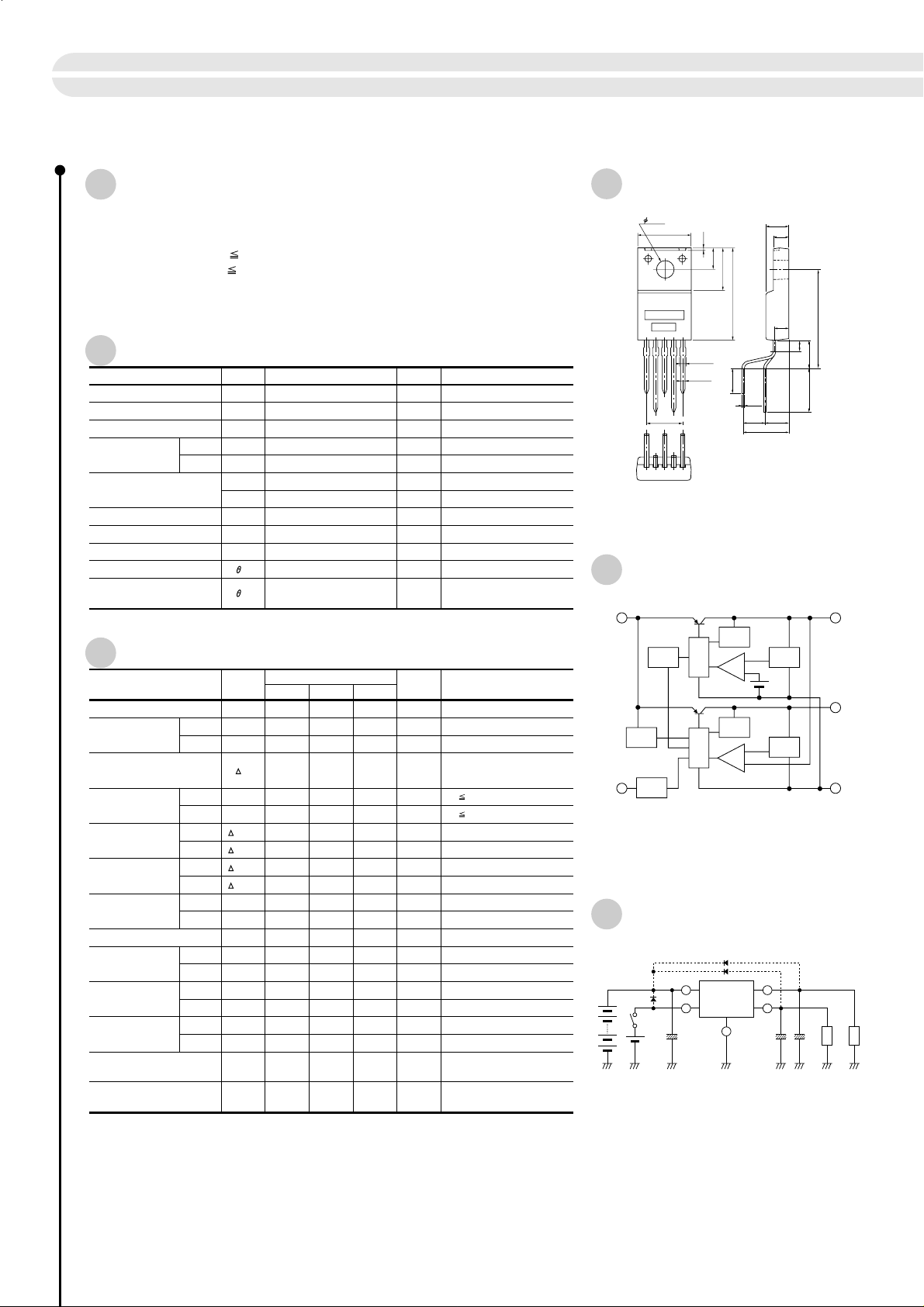
Absolute Maximum Ratings
Parameter Symbol Unit ConditionsRatings
DC input voltage
Battery reverse connection
Output control terminal voltage
Output current
CH1
CH2
Power Dissipation
Junction temperature
Operating temperature
Storage temperature
Junction to case thermal resistance
Junction to ambient-air thermal
resistance
V
V
V
I
I
P
P
T
Tstg
IN
INB
C
O1
O2
D1
D2
Tj
OP
j-c
j-a
Electrical Characteristics
Parameter Symbol
V
Input voltage
Output voltage
Channel-channel voltage difference
(V
O1
Dropout voltage
Line regulation
Load regulation
Ripple rejection
CH1
CH2
—
VO2)
CH1
CH2
CH1
CH2
CH1
CH2
CH1
CH2
Quiescent circuit current
Overcurrent protection
starting current
Output control voltage
Output control current
Overvoltage protection starting
voltage
Thermal protection starting
temperature
CH1
CH2
Output ON
Output OFF
Output ON
Output OFF
Notes:
*1. Since P
D(max)
= (V
IN
depending on operating conditions. Refer to the Ta—P
*2. Refer to the dropout voltage.
*3. I
rating shall be the point at which the output voltage VO1 or VO2 (V
S1
drops to –5%.
*4. Overvoltage protection circuit is built only in CH2 (V
*5. The indicated temperatures are junction temperatures.
*6. All terminals, except V
IN
V
O1
V
O2
V
O
V
DIF1
V
DIF2
V
O
LINE1
V
O
LINE2
V
O
LOAD1
V
O
LOAD2
R
REJ1
R
REJ2
Iq
I
(S1) 1
I
(S1) 2
V
CH
V
CL
I
CH
I
CL
V
OVP
T
TSD
– VO) • IO1+ (V
IN
IN
and GND, are open.
4.80 5.00 5.20 V
4.80 5.00 5.20 V
–0.3 5.3 V
0.06 A
0.15 A
–100 µA
– VO2) • I
35
6
*
–13
V
IN
1
0.04
*
1
0.1
*
22
1.8
–40 to +150
–40 to +105
–40 to +150
5.5
66.7
(Tj = 25ºC, VIN = 14V unless otherwise specified)
Ratings
min typ max
2
630V
*
10 50 mV
10 50 mV
30 70 mV
40 70 mV
54 dB
54 dB
3
*
3
*
4.2 4.5 4.8 V
3.2 3.5 3.8 V
4
30 V
*
5
*
151 ºC
= 22 (W), V
O2
side).
O2
V
V One minute
V
A
A
With infinite heatsink
W
Stand-alone without heatsink
W
ºC
ºC
ºC
ºC/W
Stand-alone without heatsink
ºC/W
Unit Conditions
1
*
IO = 0.04A
I
= 0.1A
O
V
=
0 to 40V, IO1 and I
IN
up to load short-circuiting
I
= 14V, I
IN
and I
O1
I
O2
V
IN
V
IN
I
O1
I
O2
= 100 to 120Hz
f
f
= 100 to 120Hz
I
O1
V
C
V
C
0.04A
0.1A
= 6 to 30V, IO = 0.04A
= 6 to 30V, IO = 0.1A
= 0 to 0.04A
= 0 to 0.1A
= 0A, VC = 0 V
= 4.8V
= 3.2V
O2 (max)
= 0.04A or I
O1
1.0 V
1.0 V
0.8 mA
100 µA
, I
IN (max)
O1(max)
curve to compute the corresponding values.
D
(Ta=25ºC)
=
0A
O2
may be limited
= 0.1A)
O2
±0.2
4.0
±0.2
7.9
1. V
2. V
3. GND
4. V
5. V
±0.3
16.9
(4.6)
IN
C (on/off)
O1
O2
(unit: mm)
4.2
2.8
2.6
+0.2
–0.1
0.45
±0.7
3.9
(4.3)
±0.7
8.2
±0.2
±0.2
±0.1
External Dimensions
±0.2
3.2
±0.2
10.0
a
b
P1.7 • 4 = 6.8
12345
±0.7 ±0.7
0.5
±0.15
0.95
+0.2
–0.1
0.85
(Forming No. 1101)
Equivalent Circuit Diagram
V
IN
1
TSD
OVP
2
CONT
V
C
DRIVE
DRIVE
OCP
ERR
OCP
ERR
DET
REF
DET
Standard Circuit Diagram
D
3
D
2
V
V
IN
1
D
1
+
C
IN
CO1 : Output capacitor (47 to 100µF, 50V)
C
: Output capacitor (47 to 100µF, 50V)
O2
*1 C
: Anti-oscillation capacitors (approx. 47µF).
IN
Tantalum capacitors are recommended, especially
2
*
D
at low temperatures.
: Protection diode.
1, D2, D3
Required as protection against reverse biasing
between input and output.
(Recommended diode: Sanken EU2Z.)
SI-3102S
2
V
C
O2
5
4
3
V
O1
GND
C
O1
(2.0)
±0.6
5.0
(8.0)
a: Type No.
b: Lot No.
++
C
O2
(17.9)
V
O1
4
5
V
O2
3
GND

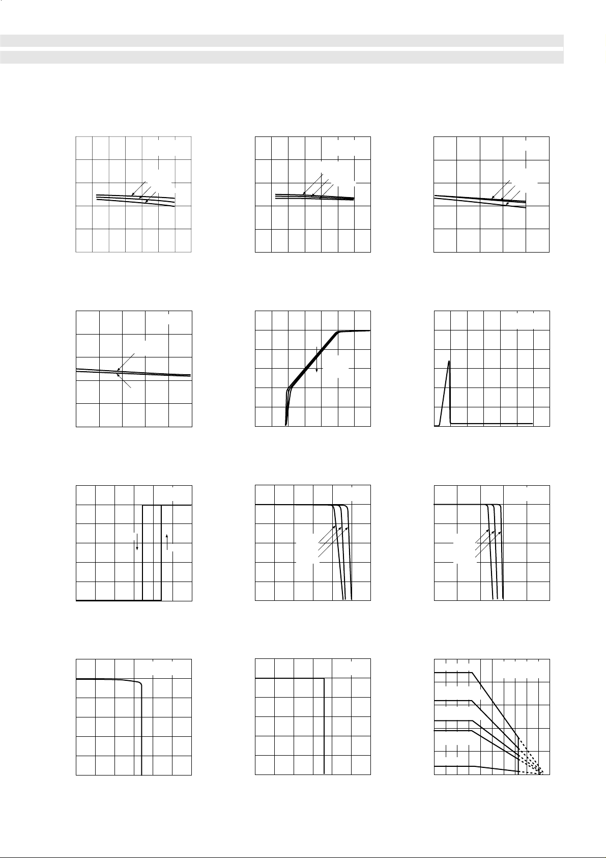
Line Regulation (1)
■
5.10
5.05
5.00
4.95
I
O1
0A
VIN = V
IO2 = 5mA
=
20mA
40mA
Line Regulation (2)
■
C
5.10
5.05
5.00
VIN = V
C
IO1 = 5mA
I
=
O2
0A
50mA
100mA
4.95
Load Regulation (1)
■
5.10
5.05
5.00
O (V)
4.95
VIN = V
C
V
=
IN
6V
14V
30V
4.90
Output voltage VO (V)
4.85
5 101520253035 0
0
Input voltage V IN (V)
Load Regulation (2)
■
5.10
5.05
=
V
IN
5.00
6V,14V
4.95
30V
4.90
Output voltage VO (V)
4.85
0
20 40 60 10080
Output current IO (mA)
ON/OFF Control Characteristics
■
6
5
4
O (V)
3
OFF
2
Output voltage V
1
VIN = V
VIN = 14V
I
= 5mA
O2
ON
4.90
Output voltage VO (V)
4.85
5 101520253035 0
Input voltage VIN (V)
Rise Characteristics
■
6
C
5
4
I
= 0 A
O (V)
3
O1
20mA
40mA
2
1
Output voltage V
0
0
123 56740
Input voltage V
Overcurrent Protection Characteristics (1)
■
6
5
IN (V) Input voltage VIN (V)
VIN = V
C
IO2 = 5mA
4
O (V)
3
2
Output voltage V
1
=
V
IN
6V
14V
30V
4.90
Output voltage V
4.85
Circuit Current
■
10 20 30 5040
Output current I
12
10
O (mA)
VC = 0 V
I
= 0A
O1
8
6
4
Ground current lg (mA)
2
0
5 1015 25303520
Overcurrent Protection Characteristics (2)
■
6
5
VIN = V
IO1 = 5mA
C
4
V
=
3
2
Output voltage VO (V)
1
IN
6V
14V
30V
0
0
12 6543
Output ON/OFF control voltage VC (V)
Thermal Protection Characteristics
■
6
5
VIN = 6 V
I
O1
= IO2 = 5mA
Overvoltage Protection Characteristics
■
4
O (V)
O (V)
3
2
Output voltage V
1
0
100
120 140 240220200180
Ambient temperature Ta (ºC)
Note on Thermal Protection Characteristics:
The thermal protection circuit is intended for protection against heat
during instantaneous short-circuiting. Its operation, including reliability,
is not guaranteed for short-circuiting over an extended period of time.
Output voltage V
0
20 40 60 12010080 0
0
Output current IO (mA)
6
5
VIN = V
C
IO2 = 5mA
4
3
2
1
0
26
28 30 38363432
Input voltage V
IN (V)
0
0.1 0.2 0.50.40.3
Output current IO (A)
Ta—PD Characteristics
■
25
With infinite heatsink
20
200 • 200 • 2mm
(2.3ºC/W)
15
100 • 100 • 2mm
(5.2ºC/W)
10
75 • 75 • 2mm
(7.6ºC/W)
5
Power Dissipation PD (W)
Without heatsink
0
–
40
–
20 0 20 16014012060 80 10040
Operating temperature Ta (ºC)
With silicone grease G746
(Shin-Etsu Chemical)
Heatsink: aluminum
17
 Loading...