Sanken Electric Co SI-3025B Datasheet

●SI-3000B Series
SI-3000B Series
5-Terminal, Multi-Function, Full-Mold, Low Dropout Voltage Dropper Type
■Features
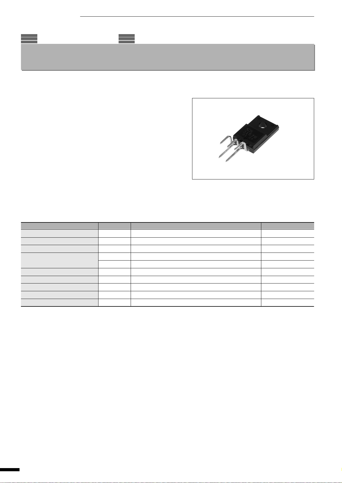
• Compact full-mold package (equivalent to TO220)
• Output current: 0.27A
• Low dropout voltage: VDIF≤0.5V (at IO=0.27A)
• Output ON/OFF control terminal is compatible with LS-TTL. (It may be directly
driven by LS-TTL or standard CMOS logic.)
• Built-in foldback overcurrent, thermal protection circuits
• Highly accurate overcurent protection starting current
SI-3157B : 0.3 to 0.7A (VIN=18V)
SI-3025B : 0.3 to 0.7A (When VIN=18V, setting VO=15.7V)
0.3 to 0.75A (When VIN=18V, setting VO=11.7V)
• Variable output voltage type (SI-3025B) also available
■Applications
• For BS and CS antenna power supplies
• Electronic equipment
■Absolute Maximum Ratings
Paarameter
DC Input Voltage
Voltage of Output Control Terminal
DC Output Current
Power Dissipation
Junction Temperature
Ambient Operating Temperature
Storage T emperature
Thermal Resistance (junction to case)
Thermal Resistance (junction to ambient air)
Symbol
VIN
VC
IO
PD1
PD2
Tj
Top
Tstg
Rth(j-c)
Rth(j-a)
Ratings
35
VIN
*1
0.27
14(With infinite heatsink)
1.5(Without heatsink, stand-alone operation)
–40 to +125
–30 to +100
–40 to +125
7.0
66.7(Without heatsink, stand-alone operation)
(Ta=25°C)
Unit
V
V
A
W
W
°C
°C
°C
°C/W
°C/W
28

●SI-3000B Series
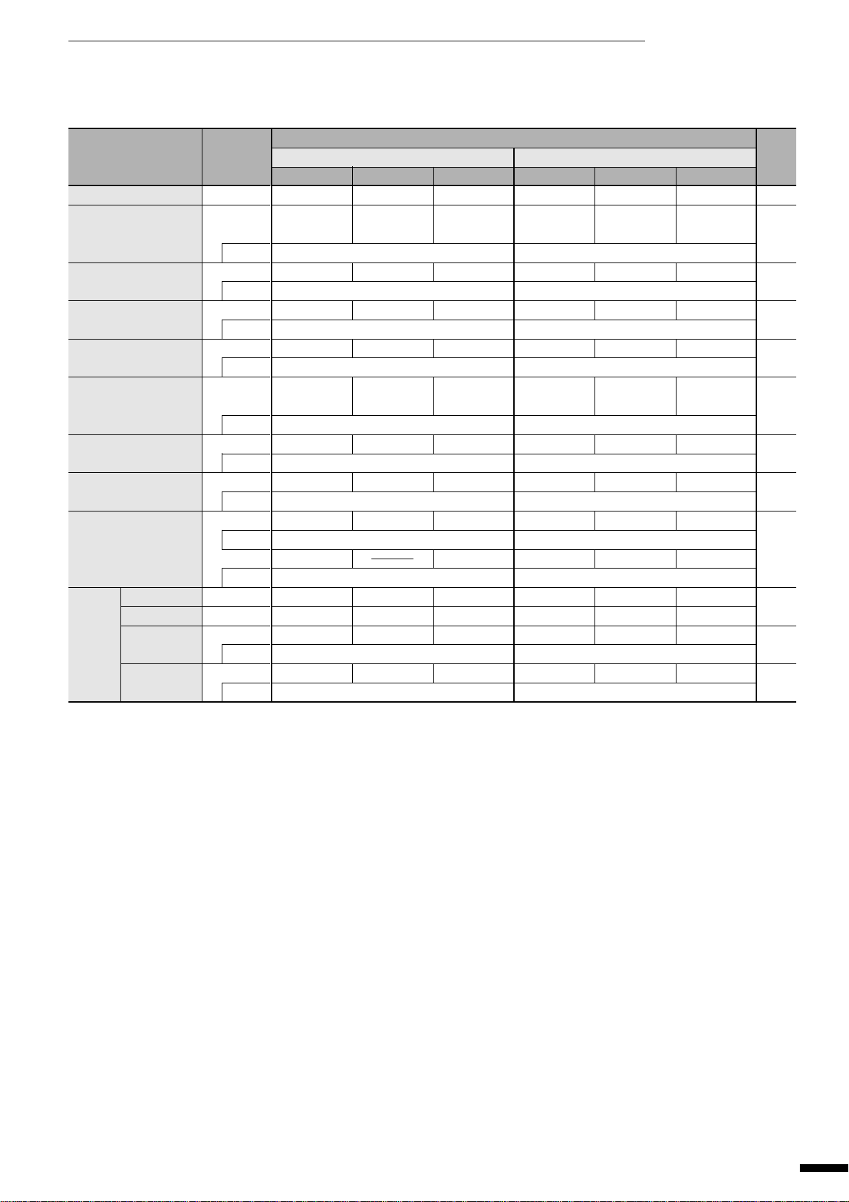
■Electrical Characteristics
(Ta=25°C unless otherwise specified)
Ratings
Parameter
Input Voltage
Output Voltage
(SI-3025B: Reference
Voltage)
Dropout Voltage
Line Regulation
Load Regulation
Temperature Coefficient of Output
Voltage (SI-3025B: Temperature
Coefficient of Reference Voltage)
Ripple Rejection
Quiescent Circuit
Current
Overcurrent Protection
Starting Current
*3,4
Control Voltage (Output ON)
Control Voltage (Output OFF)
VC
Control Current
Terminal*5(Output ON)
Control Current
(Output OFF)
Symbol
VIN
(VREF)
Conditions
VDIF
Conditions
∆VOLINE
Conditions
∆VOLOAD
Conditions
∆VO/∆Ta
(∆V
REF
Conditions
RREJ
Conditions
Conditions
Conditions
Conditions
VC. IH
VC. IL
IC. IH
Conditions
IC. IL
Conditions
VO
IS1
Iq
/∆Ta)
SI-3157B
min. typ. max.
*2
27
*1
14.92 15.70 16.48
VIN=18V, IO=0.2A
0.5
IO≤0.27A
30 90
VIN=17 to 27V, IO=0.2A
120 300
VIN=18V, IO=0 to 0.27A
±1.5
VIN=18V, IO=5mA, Tj=0 to 100°C
54
VIN=18V, f=100 to 120HZ
310
VIN=18V, IO=0A
0.3 0.7
VIN=18V
2.0
0.8
20
VC=2.7V
–0.3
VC=0.4V
SI-3025B
min. typ. max.
*2,6
6
27
*1
2.448 2.550 2.652
VIN=VO+3V, IO=0.2A
0.5
IO≤0.27A
10
VIN=(VO+1) to 27V, IO=0.27A
10
VIN=VO+3V, IO=0 to 0.27A
±0.5
VIN=VO+3V, IO=5mA, Tj=0 to 100°C
54
VIN=VO+3V, f=100 to 120HZ
310
VIN=VO+3V, IO=0A
0.3 0.75
When VIN=18V, setting VO=11.7V
0.3 0.7
When VIN=18V, setting VO=15.7V
2.0
0.8
20
VC=2.7V
–0.3
VC=0.4V
Unit
V
V
V
mV
(3025B:
mV/V)
mV
(3025B:
mV/V)
mV/°C
dB
mA
A
V
µA
mA
*1: VIN(max) and IO(max) are restricted by the relation PD(max)=(VIN-VO)•IO=14(W).
*2: Refer to the dropout voltage.(Refer to Setting DC Input Voltage on page 7.)
*3: IS1 is specified at –5(%) drop point of output voltage VO on the condition that VIN=VO+3V, IO=0.2A.
*4: A f oldbac k type o v ercurrent protection circuit is b uilt into the IC regulator. Therefore, avoid using it f or the following applications as it may cause
starting errors:
(1) Constant current load (2) Plus/minus power (3) Series power (4) VO adjustment by raising ground voltage
*5: Output is ON even when output control terminal VC is open. Each input level is equivalent to LS-TTL. Therefore, it may be directly driven by an
LS-TTL circuit.
*6. When setting output voltage to 5V or less, input voltage needs to be set to 6V or over to operate stably.
29
 Loading...