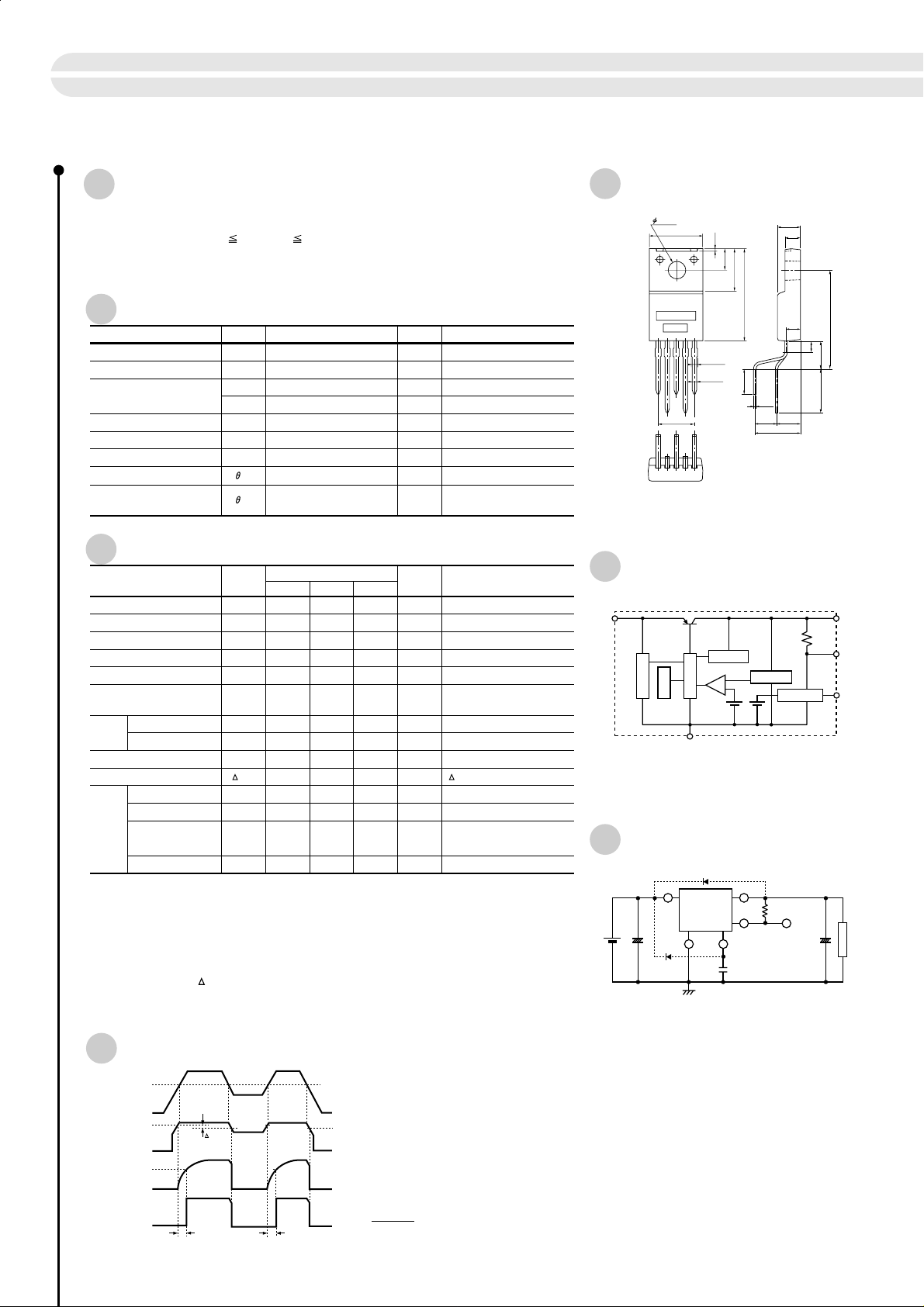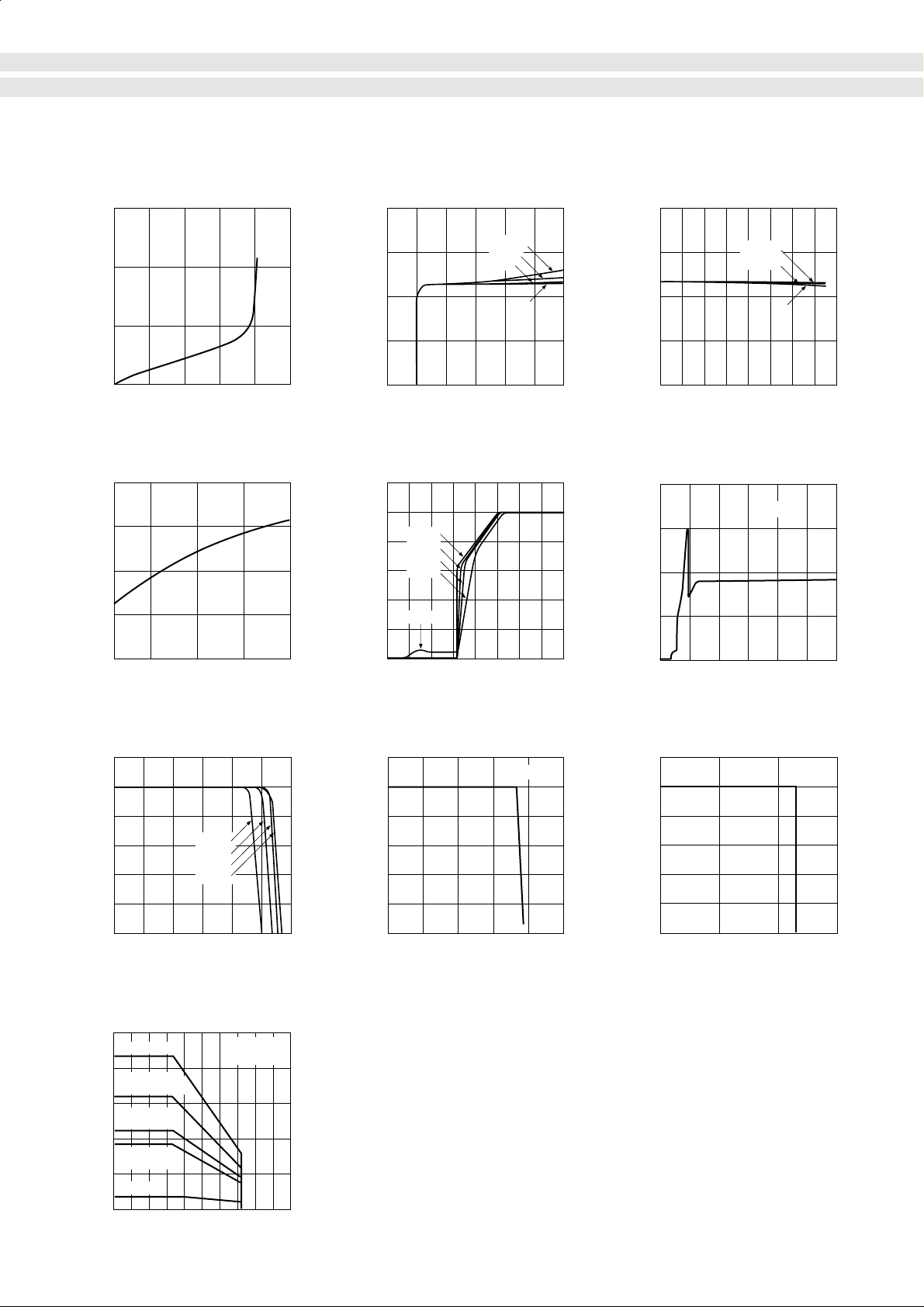
Dropper Type Regulator with Reset Function SI-3011S
10
Features
● 5-terminal IC regulator with reset function; 0.7A output current
● Voltage accuracy of ±2%
● Low Dropout voltage 0.5V at IO 0.3A
●
Built-in constant current type overcurrent, overvoltage and thermal protection circuits
● TO-220 equivalent full-mold miniature package
Absolute Maximum Ratings
Parameter Symbol Unit ConditionsRatings
DC input voltage
Output current
Power Dissipation
Junction temperature
Operating temperature
Storage temperature
Junction to case thermal resistance
Junction to ambient-air thermal
resistance
Electrical Characteristics
Parameter Symbol
Input voltage
Output voltage
Dropout voltage
Ripple rejection
Quiescent circuit current
Overcurrent protection starting
current
Threshold voltage
DLY
terminal
Source current
Reset threshold voltage level
Reset threshold voltage hysteresis
H-level output voltage
L-level output voltage
6
*
V
RST
Source current when
terminal
H-level
Sink current when L-level
Notes:
*1. Since P
conditions. Refer to the Ta—P
*2. Refer to the dropout voltage.
*3. I
rating shall be the point at which the output voltage VO (VIN = 14V, Io = 0.3A) drops to –5%.
S
thL is the Vo threshold voltage at which the V
*4. V
O
*5. V
thH is the Vo threshold voltage at which the V
O
given by V
*6. Reset signal output terminal V
connection with a logic circuit.
= (V
D(max)
thL plus VOth.
O
IN –VO
V
I
P
P
Tj
T
Tstg
IN
O
D1
D2
OP
j-c
j-a
35
0.7
22
1.8
–40 to +150
–40 to +105
–40 to +150
5.5
66.7
1
*
A
With infinite heatsink
W
Stand-alone without heatsink
W
ºC
ºC
ºC
ºC/W
Stand-alone without heatsink
ºC/W
V
(Tj=25ºC, VIN=14V, IO=0.3A unless otherwise specified)
Ratings
min typ max
2
V
IN
V
O
V
DIF
R
REJ
Iq
I
S
V
DLY
I
DLY
VothL
V
o
V
RSTH
V
RSTL
I
RSTH
I
RSTL
) • IO = 22 (W), V
RST
*
630V
4.90 5.00 5.10 V
54
8.5
3
*
0.71 A
th
4
*
VO •
th
VO–
2.9
2.7
35
25
VO •
0.92
0.90
50
VO •
100
0.1
1.3
and I
IN (max)
curve to compute the corresponding values.
D
O(max)
terminal turns from high to low.
RST
terminal turns from low to high. VothH may be
RST
is pulled up in the IC [pull-up resistance 3 k Ω (typ)], allowing direct
Unit Conditions
1
*
0.5 V
f = 100 to 120Hz
dB
12 mA
3.1
45
0.94
150
0.5
–10
IO = 0 A
DLY terminal open
V
µA
V
V
VOth = VOthH – VOthL
mV
V
V
V
VO =
VO =
mA
shorted across V
mA
V
= 5.0V (typ
O
=
5.0V (typ)
O
5.0V (typ)
5.0V (typ)
=
0.5V
RST
may be limited depending on operating
)
5
*
, RL =
, RL =
,
(Ta=25ºC)
510Ω
510Ω
and GND
RST
Reset Signal Output Timing Chart
V
IN
VO + V
GND
GND
0 (V)
0 (V)
DIF
V
O
V
OthH
V
DLYth
t
DLY
V
OthL
V
Oth
V
DLY
V
RSTH
V
RSTL
t
DLY
[Calculating t
Reset signal delay time tDLY is calculated from the following formula:
t
DLY
]
DLY
V
+ 0.2
DLYth
=
• C
DLY
* I
is the current flowing from DLY terminal
I
DLY
DLY
shown in the Standard Circuit Diagram.
Input voltage
Output voltage
Voltage across
delay capacitor
Reset signal output
External Dimensions
±0.2
3.2
±0.2
10.0
a
b
0.95
0.85
±0.7
±0.7
P1.7
•4 = 6.8
12345
(unit: mm)
0.5
±0.2
4.0
±0.2
7.9
±0.3
16.9
±0.15
+
0.2
---
0.1
(4.6)
+
0.2
---
0.1
0.45
±0.7
3.9
8.2
Terminal connections
1. V
IN
2. V
RST
3. GND
4. DLY
5. V
OUT
(Forming No. 1101)
Equivalent Circuit Diagram
V
IN
1
OCP
OVP
TSD
GND
DRIVE
1
ERR
REF1 REF2
DET
Standard Circuit Diagram
2
*
D
1
15
V
IN
1
Power
*
C
1
supply
+
Co : Output capacitor (47 to 100µF, 50V)
*1 C
: Anti-oscillation capacitors (C1: approx. 47µF).
1
This must be connected to terminals 1 (V
via the shortest possible routing. An approximately
0.33µF capacitor with good high frequency
characteristics must be connected in parallel in case of
inductive input lines or long-distance wiring. Tantalum
capacitors are recommended for C
at low temperatures.
2
*
D1,D2 : Protection diode.
Required as protection against reverse biasing between
input and output.
(Recommended diode: Sanken EU2Z.)
SI-3011S
3
GND
2
*
D
2
V
OUT
R
2
4
V
RST
Reset signal
output terminal
DLY
C
DLY
±0.2
4.2
±0.2
2.8
±0.1
2.6
(17.9)
(2.0)
±0.6
5.0
(8.0)
(4.3)
±0.7
a: Type No.
b: Lot No.
RESET
L
C
O
+
) and 3 (GND)
IN
and C0, especially
1
V
OUT
5
V
RST
2
DLY
4
Load

Io vs V
■
DIF
1.5
Characteristics
Line Regulation
■
5.10
Load Regulation
■
5.10
1.0
0.5
Dropout voltage VDIF (V)
0
0 0.2 0.4 0.6 0.8 1.0
Output current IO (A)
Output Voltage Temperature Characteristics
■
5.1
O (V)
5.0
Output voltage V
4.9
–40 0 50 100 150
Ambient temperature Ta (ºC)
5.05
5.00
4.95
Output voltage VO (V)
4.90
Rise Characteristics
■
51015202530
0
Input voltage V IN (V)
6
5
IO = 0 A
4
0.1A
0.3A
3
0.7A
2
IO = 0 A
1
0
0
2468
Input voltage V
IO=0.1A
0.3A
0.7A
5.05
O (V)
0A
5.00
VIN=14V
4.95
Output voltage V
4.90
0
0.2 0.4 0.6 0.8
Output current I
Quiescent Circuit Current
■
20
15
10
5
Quiescent current lq (mA)
0
0
51015202530
IN (V) Input voltage VIN (V)
10V
6V
O (A)
IO = 0 A
Overcurrent Protection Characteristics
■
6
5
4
O (V)
3
2
Output voltage V
1
0
0
Output current I
Ta—PD Characteristics
■
25
With infinite heatsink
20
200 • 200 • 2mm
(2.3ºC/W)
15
100 • 100 • 2mm
(5.2ºC/W)
VIN = 6 V
10V
14V
16V
0.5 1.0 1.5 25
O (A)
With silicone grease
Heatsink: aluminum
10
75 • 75 • 2mm
(7.6ºC/W)
5
Power Dissipation PD (W)
Without heatsink
0
–40 0 40 80 120 160
Operating temperature Ta (ºC)
Thermal Protection Characteristics
■
Overvoltage Protection Characteristics
■
6
IO = 5mA
5
4
O (V) Output voltage VO (V)
O (V)
3
2
Output voltage V
1
0
100 150 200
Ambient temperature Ta (ºC)
Output voltage V
Note on Thermal Protection Characteristics:
The thermal protection circuit is intended for protection
against heat during instantaneous short-circuiting. Its
operation, including reliability, is not guaranteed for
short-circuiting over an extended period of time.
6
5
4
3
2
1
0
I
OUT
30 35 40
Input voltage V
IN (V)
= 5mA
11
 Loading...