Sanken Electric Co SI-3003S Datasheet

3-terminal Dropper Type Regulator SI-3003S
Features
● 3-terminal IC regulator with 0.8A output current
● Voltage accuracy of ±2%
● Low Dropout voltage 0.5V at I
Built-in constant current type overcurrent, overvoltage and thermal protection circuits
●
● TO-220 equivalent full-mold package
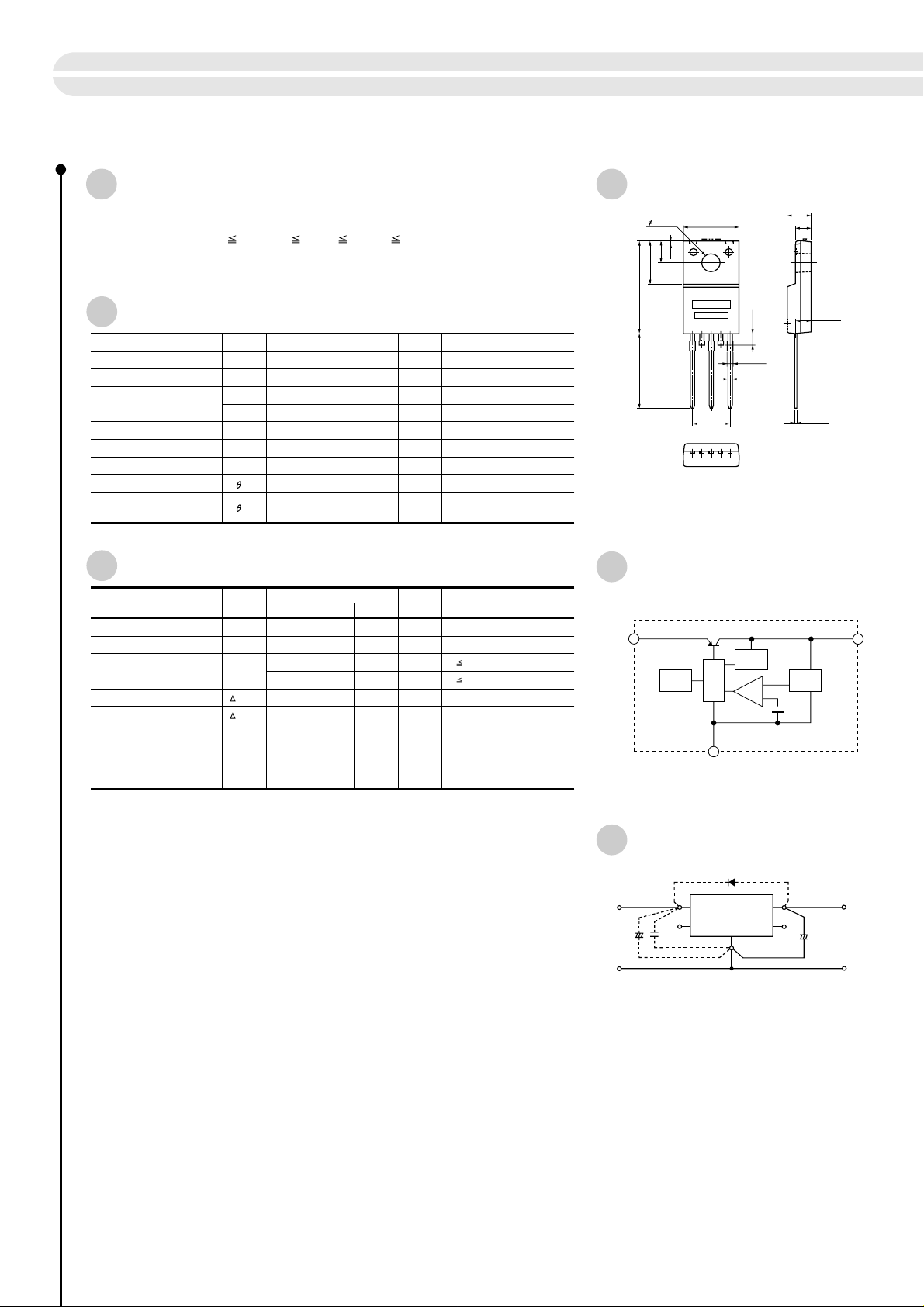
Absolute Maximum Ratings
Parameter Symbol Unit ConditionsRatings
DC input voltage
Output current
Power Dissipation
Junction temperature
Operating temperature
Storage temperature
Junction to case thermal resistance
Junction to ambient-air thermal
resistance
V
P
P
T
Tstg
IN
I
O
D1
D2
Tj
OP
j-c
j-a
Electrical Characteristics
Parameter Symbol
V
V
V
V
R
V
DIF
O LINE
O
REJ
Iq
I
S1
IN
O
Input voltage
Output voltage
Dropout voltage
Line regulation
Load regulation
Ripple rejection
Quiescent circuit current
Overcurrent protection starting
current
Notes:
*1. Since P
= (VIN–VO) • IO=22 (W), V
D(max)
conditions. Refer to the Ta—P
*2. Refer to the dropout voltage.
*3. IS1 rating shall be the point at which the output voltage V
0.5A, 1V at IO 0.8A
O
35
0.8
22
1.8
–40 to +150
–40 to +100
–40 to +150
5.5
66.7
2
*
V
A
W
W
ºC
ºC
ºC
ºC/W
ºC/W
(Tj=25ºC, VIN=14V, IO=0.5A unless otherwise specified)
Ratings
min typ max
2
630V
*
4.90 5.00 5.10 V
LOAD
54
3
3
*
0.9 A
and I
IN(max)
curve to compute the corresponding values.
D
O(max)
Unit Conditions
1
*
0.5
1.0
V
V
30 mV
100 mV
dB
10 mA
may be limited depending on operating
(VIN=14V, IO=0.5A) drops to –5%.
O
(Ta=25ºC)
With infinite heatsink
Stand-alone without heatsink
Stand-alone without heatsink
IO 0.5A
0.8A
I
O
=8 to 16V
V
IN
I
=0 to 0.5A
O
f=100 to 120Hz
=0A
I
O
±0.2
0.94
0.85
(unit: mm)
2 max
±0.15
+0.2
–0.1
Terminal connections
1. V
IN
2. (NC)
3. GND
4. (NC)
5. V
O
(Forming No. 1115)
External Dimensions
±0.2
±0.3
16.9
(13.5)
±0.15
4•P1.7
(root dimensions)
3.2
±0.2
7.9
±0.2
4
=6.8
0.5
a
±0.15
10
b
12345
Equivalent Circuit Diagram
V
IN
1
TSD
GND
DRIVE
3
OCP
ERR
Standard Circuit Diagram
2
D
*
1
4.2
2.8
REF
±0.2
±0.2
DET
±0.15
2.6
+0.2
–0.1
0.45
a: Type No.
b: Lot No.
V
O
5
1
SI-3003S
1
+
*
DC input
C
V
IN
Co : Output capacitor (47 to 100µF, 50V)
1
C
: Anti-oscillation capacitors (C1: approx. 47µF, C2: approx.
1,C2
*
0.33µF). These are required for inductive input lines or
long wiring. Tantalum capacitors are recommended for
and Co, especially at low temperatures.
C
1
2
: Protection diode. Required as protection against reverse
D
*
1
biasing between input and output.
(Recommended diode: Sanken EU2Z.)
2
N.C N.C
C
2
1
5
4
3
+
DC output
C
O
V
O
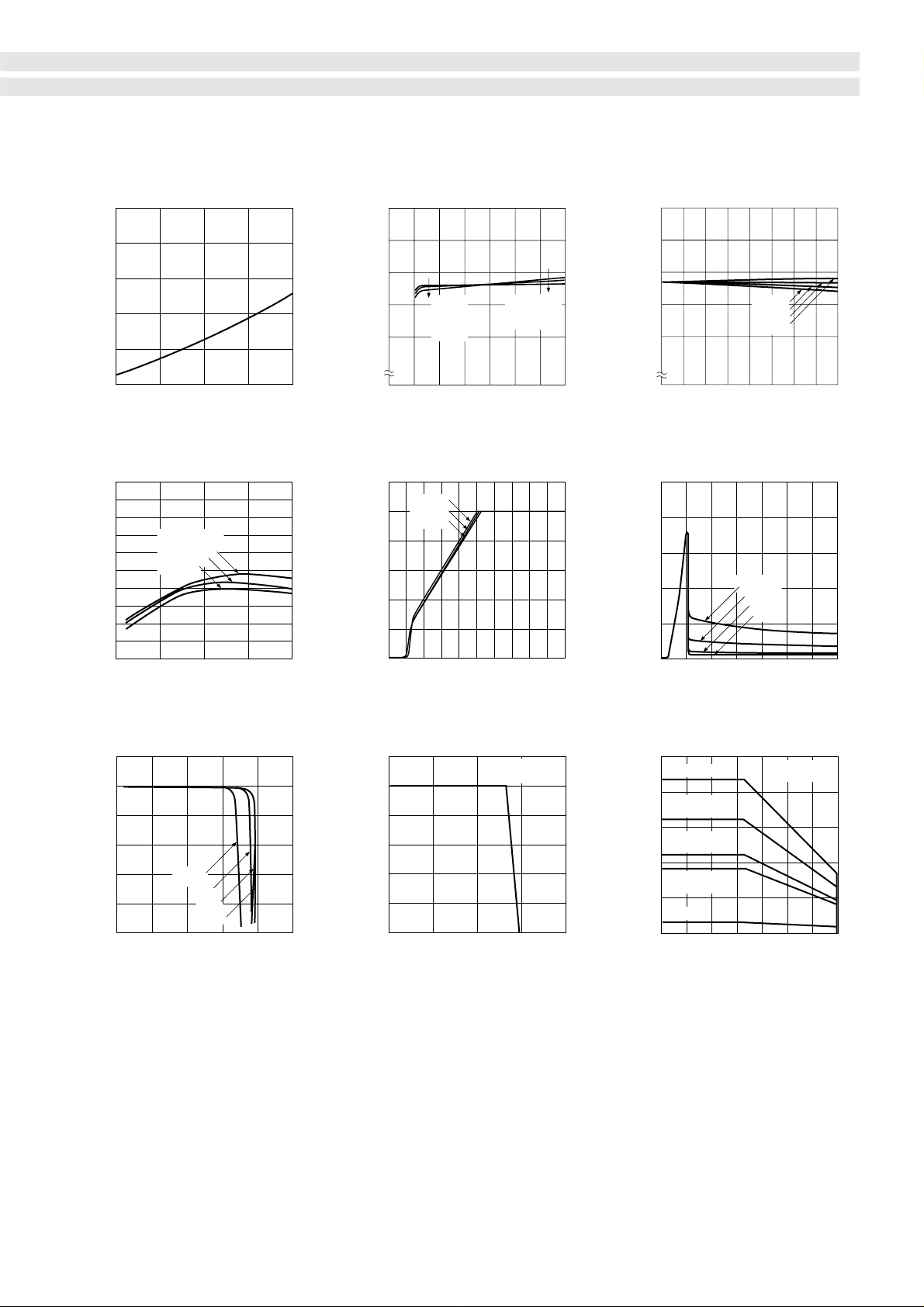
8

Io vs V
■
0.5
0.4
Characteristics
DIF
Line Regulation
■
5.1
Load Regulation
■
5.1
0.3
0.2
0.1
Dropout voltage VDIF (V)
0
0 0.2 0.4 0.6 0.8
Output current IO (A)
Output Voltage Temperature Characteristics
■
5.1
VIN / IO:
30V / 0A
O (V)
5.0
Output voltage V
4.9
–50 0 50 100 150
14V / 0.5A
6V / 0.8A
Ambient temperature Ta (ºC)
5.0
IO=0A
4.9
Output voltage VO (V)
0
0
5 10152025 3530
Input voltage VIN (V)
Rise Characteristics
■
6
IO=0A
=0.5A
5
=0.8A
4
O (V)
3
2
1
Output voltage V
0
246 108
0
Input voltage V
=0.2A
=0.5A
=0.8A
5.0
O (V)
IO=0.5, 0.8A
=0.2A
=0A
4.9
Output voltage V
0
0
Circuit Current
■
0.2 0.4 0.6 0.8
VIN=
=
=
=
Output current I
250
200
150
IO=
100
50
Ground current lg (mA)
0
0
5 1015 2025 3530
IN (V) Input voltage VIN (V)
0.8A
=
0.5A
=
=
0.2A
0A
35V
25V
14V
6V
O (A)
Overcurrent Protection Characteristics
■
6
5
4
O (V)
3
2
Output voltage V
1
0
0
VIN=6V
14V
35V
25V
0.5 1.0 1.5 2.0 2.5
Output current I
O (A)
Ta—PD Characteristics
Thermal Protection Characteristics
■
6
5
VIN=6V
I
=5mA
O
■
4
O (V)
3
2
Output voltage V
1
0
120 140 160 180 200
Ambient temperature Ta (ºC)
Power Dissipation PD (W)
Note on Thermal Protection Characteristics:
The thermal protection circuit is intended for protection
against heat during instantaneous short-circuiting. Its
operation, including reliability, is not guaranteed for
short-circuiting over an extended period of time.
25
With infinite heatsink
20
200 • 200 • 2mm
(2.3ºC/W)
15
100 • 100 • 2mm
(5.2ºC/W)
With silicone grease
Heatsink: aluminum
10
75 • 75 • 2mm
(7.6ºC/W)
5
Without heatsink
0
–40 0 40 80 100
Operating temperature Ta (ºC)
9
 Loading...