Dropper Type Regulator with Output On/Off Control SI-3001S
Features
Output current of 1.0A
●
5-terminal type <output on/off control, variable output voltage (rise only)>
●
Voltage accuracy of ±2%
●
Low dropout voltage 1V at I
●
Built-in overcurrent, overvoltage and thermal protection circuits
●
Withstands external electromagnetic noises
●
TO-220 equivalent full-mold package
●
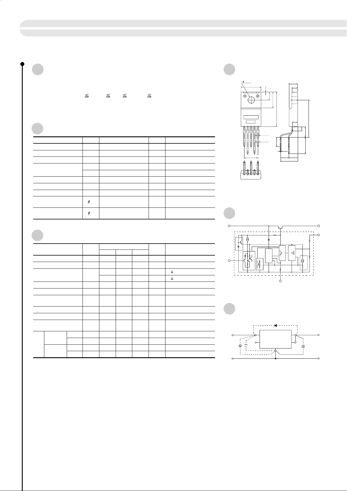
Absolute Maximum Ratings
Parameter Symbol Unit ConditionsRatings
DC Input Voltage
Output Control Terminal Voltage
Output Current
Power Dissipation
Junction Temperature
Operating Temperature
Storage Temperature
Junction to Case Thermal
Resistance
Junction to Ambient-Air Thermal
Resistance
V
V
P
P
T
Tstg
IN
C
I
O
D1
D2
Tj
OP
j-c
j-a
Electrical Characteristics
Parameter Symbol
V
Input Voltage
Output Voltage
Dropout Voltage
Line Regulation
Load Regulation
Output Voltage Temperature
Coefficient
Ripple Rejection
Quiescent Circuit Current
Overcurrent Protection Starting
Current
Control Voltage
Control Current
Vc Terminal
Output ON
Output OFF
Output ON
Output OFF
Notes:
*1. Since P
(max)=(V
D
IN–VO
conditions. Refer to the Ta-P
*2. Refer to the dropout voltage.
S1 rating shall be the point at which the output voltage V
*3. I
*4. The output control terminal Vc is pulled up inside the IC. Each input level can be directly driven with
LS-TTL ICs. Thus, LS-TTL direct driving is also possible.
IN
V
O
V
DIF
∆V
O LINE
∆V
O
LOAD
R
REJ
Iq
I
S1
V
C, IH
V
C, IL
I
C, IH
I
C, IL
)•IO=18( W), V
curve to compute the corresponding values.
D
1.0A, 0.5V at I
O
35
V
1.0
18
1.5
– 40 to +125
– 40 to +100
– 40 to +125
5.5
66.7
IN
1
*
O
0.4A
V
V
A
With infinite heatsink
W
Stand-alone without heatsink
W
ºC
ºC
ºC
ºC/W
Stand-alone without heatsink
ºC/W
(Ta=25ºC, VIN=14V unless otherwise specified)
Ratings
min typ max
2
6
*
4.90 5.00 5.10 V
±0.5
54
3
3
*
1.2 A
4
*
2.0 V
(max)and IO(max)may be limited depending on operating
IN
Unit Conditions
30 *1V
VIN=12 to 16V, IO=0.4A
0.5
1.0
30 mV
100 mV
10 mA
V
V
mV/ºC∆VO/∆T
dB
I
O
I
1.0A
O
IO=0.4A, VIN=6 to 16V
=0 to 0.4A
I
O
=5mA, Ta = –10 to +100ºC
I
O
f=100 to 120Hz
=0A
I
O
0.4A
0.8 V
=2.7V
20
–0.3µAmA
(VIN = 14V, Io = 0.4A) drops to –5%.
O
V
V
C
=0.4V
C
(Ta=25ºC)
0.2
±
4.0
0.2
±
7.9
0.3
±
(4.6)
1. GND
2. V
3. V
4. V
5. V
16.9
0.45
3.9
C (on/off)
o
osense
IN
(unit: mm)
0.2
±
4.2
0.2
±
2.8
0.1
±
2.6
+
0.2
–
0.1
±
0.7
(4.3)
0.7
±
8.2
0.6
(2.0)
±
5.0
(8.0)
a: Type No.
b: Lot No.
External Dimensions
±
0.2
3.2
±
0.2
10.0
a
b
P1.7
12345
0.5
±
0.15
0.95
+
0.2
–
0.1
0.85
±
±
0.7
0.7
•4 =6.8
(Forming No. 1101)
Equivalent Circuit Diagram
Tr
5
V
IN
a
2
Vc
(on/off)
a : Pre-regulator
b : Output ON/OFF control
c : Thermal protection
d : Over-input and overcurrent protection
b
c
1
GND
e
R
2
1
MIC
f
g
e : Drive circuit
f : Error amplifier
g : Reference voltage
R
1
d
Standard Circuit Diagram
D
1
53
SI-3001S
OPEN
+
DC input
C
V
IN
Co : Output capacitor (47 to 100µF, 50V)
C
, C2 : Anti-oscillation capacitors (C1: approx. 47µF, C2: approx.
1
0.33µF). These are required for inductive input lines or
long wiring. Tantalum capacitors are recommended for C
and Co, especially at low temperatures.
: Protection diode. Required as protection against reverse
D
1
biasing between input and output.
(Recommended diode: Sanken EU2Z.)
24
C
2
1
1
+
C
(17.9)
O
R
3
R
4
DC output
3
V
O
4
V
sense
O
V
O
1
6

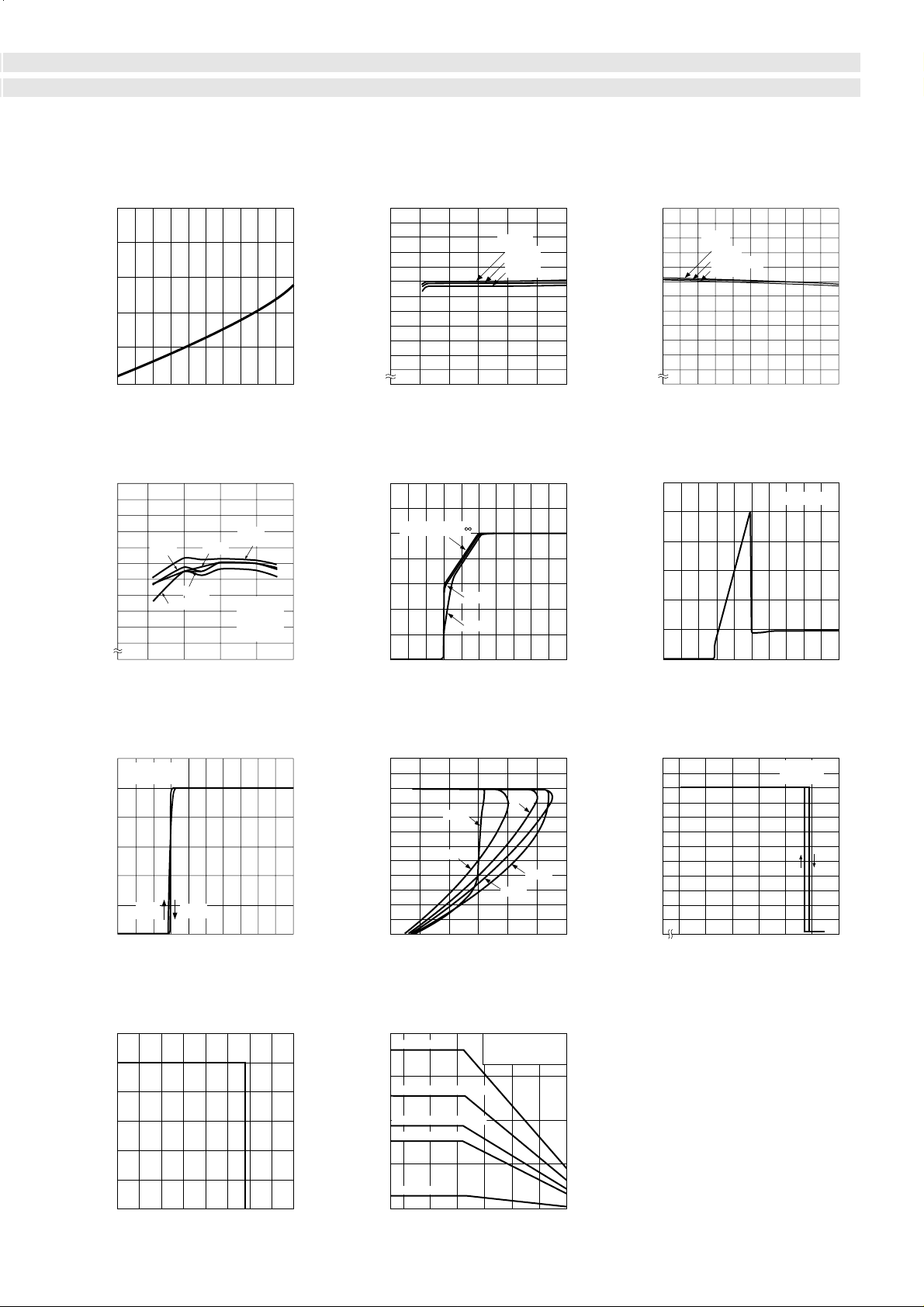
Io vs V
■
DIF
0.5
0.4
0.3
0.2
Characteristicsc
Line Regulation
■
5.1
5.0
I
O =
0 (A)
0.4 (A)
1.0 (A)
Load Regulation
■
5.1
5.0
O (V)
=
V
IN
30 (V )
12 to 16 (V )
5.5 (V )
0.1
Dropout voltage VDIF (V)
0
0
Output Voltage Temperature Characteristics
■
0.5 1.0
Output current IO (A)
5.1
V
IN =
O (V)Output voltage VO (V)Output voltage VO (V)
5.0
16(V)
12(V)
14(V)
5.5(V)
Output voltage V
4.9
0
ON/OFF Control Characteristics
■
6
I=0 (A)
o
V
5
0
Ambient temperature Ta (ºC)
=
14 (V)
IN
30(V)
VIN—IOUT condition
1.05.5
(V) (A)
/
(V)
(A)
0.412
/
(V)
(A)
0.414
/
0.416
(V)
(A)
/
030
(V)
(A)
/
100--50 50 150
4
3
2
1
0
0
Output ON/OFF control voltage VC (V)
OFF
ON
123
45
Output voltage VO (V)
4.9
0051015202530
Input voltage VIN (V)
Rise Characteristics
■
7
6
Load resistance
5
4
O (V)
3
(Ω)
2
Output voltage V
1
12
5
Ω)
(
00246810
Input voltage V
Overcurrent Protection Characteristics
■
IN (V) Input voltage VIN (V)
6
5
4
O (V)
3
2
Output voltage V
1
30
(V)
5.5
(V)
10
(V)
20
14
(V)
000.5 1.0 1.5 2.0
Output current I
O (A)
(V)
2.5 3.0
Output voltage V
4.9
0
0
Circuit Current
■
0.5
Output current I
O (A)
15
10
5
Ground current lg (mA)
0
246810
0
Thermal Protection Characteristics
■
6
5
4
O (V)
3
2
Output voltage V
1
00125
130 135 140 145 150 155
Ambient temperature Ta (ºC)
I=0(A)
o
I=0
(A)
o
=
V
6
IN
1.0
(V)
Overvoltage Protection Characteristics
■
6
5
4
3
2
1
0
10
Input voltage V
3020 40 50
IN (V)
Ta—PD Characteristics
■
20
With infinite heatsink
15
200•200•2mm (2.3ºC/W)
100•100•2mm (5.2ºC/W)
10
75•75•2mm (7.6ºC/W)
5
Power Dissipation PD (W)
Without heatsink
0
0–20--30 20 6040 80 100
Operating temperature Ta (ºC)
Use G746 silicone grease
(Shin-Etsu Chemical) and
aluminum heatsink.
Note on Thermal Protection Characteristics:
The thermal protection circuit is intended for protection
against heat during instantaneous short-circuiting. Its
operation, including reliability, is not guaranteed for
short-circuiting over an extended period of time.
7
 Loading...