Sanken Electric Co SDH04 Datasheet

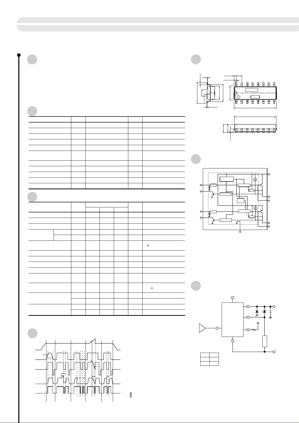
Surface-mount Dual Circuit High-side Power Switch Array SDH04
Features
● Built-in diagnostic function to detect short and open circuiting of loads and
output status signals
● Low saturation PNP transistor use
● Allows direct driving using LS-TTL and C-MOS logic levels
● Built-in overcurrent and thermal protection circuits
● Built-in protection against reverse connection of power supply
● Tj = 150ºC guaranteed
● Surface-mount full-mold package
Absolute Maximum Ratings
Parameter Symbol Unit ConditionsRatings
Power supply voltage
Drive terminal applied voltage
Input terminal voltage
DIAG output applied voltage
DIAG output source current I
Voltage across power supply
and drive terminal
Output current I
Power dissipation
Junction temperature
Operating temperature
Storage temperature
V
V
T
Tstg
V
V
V
DIAG
DIAG
P
B
D
IN
B–D
O
D
Tj
OP
Electrical Characteristics
Parameter Symbol
V
Operating power supply voltage
Quiescent circuit current
Threshold input voltage
Input current
Hi output
Lo output
Saturation voltage of output
transistor
Output terminal sink current VO = 0V, V
Saturation voltage of DIAG output
Leak current of DIAG output V
Open load detection resistor
Overcurrent protection starting
current
Thermal protection starting
temperature
Output transfer time
DIAG output transfer time
Note: * The rule of protection against reverse connection of power supply is VB = –13V, one minute
(all terminals except, V
Bopr
Iq
th
IN
I
IN
I
IN
CE (sat)
O (off)
DL
DGH
Ropen
S
T
TSD
T
ON
T
OFF
T
PLH
T
PHL
and GND, are open).
B
–13 to +40
B
–0.3 to +7.0
–0.3 to +7.0
V
–0.4
B
2.6
–40 to +150
–40 to +100
–40 to +150
(V
=14V, Ta=25ºC unless otherwise specified)
Bopr
Ratings
min typ max
6.0
16
5 12
0.8
3.0 VV
1.0
0
1
100
30
1.6
150
8 30
15
30
30
10
15
30
V
V–0.3 to V
V
V
mA 3
V
A1.5
Without heatsink, all circuits operating
W
ºC
ºC
ºC
Unit Conditions
V
L
o output
mA
V
mA
= 5 V
IN
V
= 0 V
µA
IN
VV
I
1.0A, V
O
VV
I
= 3mA0.3
DIAG
= 5 V100 µAI
DIAG
kΩ
AI
V
= V
O
Bopr
ºC
V
6V
Bopr
µS
I
= 1 A
O
µS
I
= 1 A
O
µS
I
= 1 A
O
I
= 1 A
µS
O
Bopr
IN
–1.9V
(Ta=25ºC)
= 6 to 16V0.5
= 0 V2.0 mAI
Diagnostic Function
V
B
GND
3.0V
0.8V
V
IN
GND
V
OUT
GND
I
O
SHORT
Is
OVER
VOLTAGE
OPENOPEN
TSD
External Dimensions
±0.15
2.54
+0.15
–0.05
0.89
+0.15
–0.05
0.75
16
±0.2
±0.5
6.3
8.0
6.8max
Pin 1 8
±0.2
3.6
4.0max
±0.2
1.4
0.25
±0.3
1.0
±0.3
±0.2
9.8
3.0
0 to 0.15
0.3
(unit: mm)
±0.25
a
b
20.0max
19.56
SMD-16A
±0.2
a: Type No.
b: Lot No.
Equivalent Circuit Diagram
The MIC is bound by the dotted lines.
2
IN1
3
DIAG1
7
IN2
6
DIAG2
[Abbreviations]
Drive: Drive circuit
CONT: ON/OFF circuit
Pre.Reg: Pre-regulator
*1. The base terminal (D terminal) is connected to the output
transistor base. It is also connected to the control monolithic
IC. Do not, therefore, apply an external voltage in operation.
*2. SDH04 have two or three terminals of the same function (
Out1, Out2
shorted at a pattern near the product.
Pre. Reg.
CONT.
11kΩ typ.
CONT.
11kΩ typ.
DIAG DET.
DIAG DET.
Drive
T.S.D
Drive
4,5,13
2
*
GND
DIAG.DET.: Diagnostic circuit
O.C.P.: Overcurrent protection
T.S.D.: Thermal protection
, GND). The terminals of the same function must be
O.C.P
O.C.P
9,12,16
1,15
14
8,10
11
Standard Circuit Diagram
P
Z
D
1
Out
SDH04
IN
Truth table
VINV
O
HH
LL
Note 1: A pull-down resistor (11 kΩ typ.) is connected to the IN terminal.
V
turns "L" when a high impedance is connected to the IN terminal in
OUT
series.
DIAG
5.1kΩ
V
CC
Load
V
B
Out1
D1
Out2
D2
VB,
GND
9
2
*
2
*
1
*
2
*
1
*
V
B
30
GND
V
DIAG
Normal Shorted load Open load Overvoltage Overheat
ERROR SIGNAL for CPU

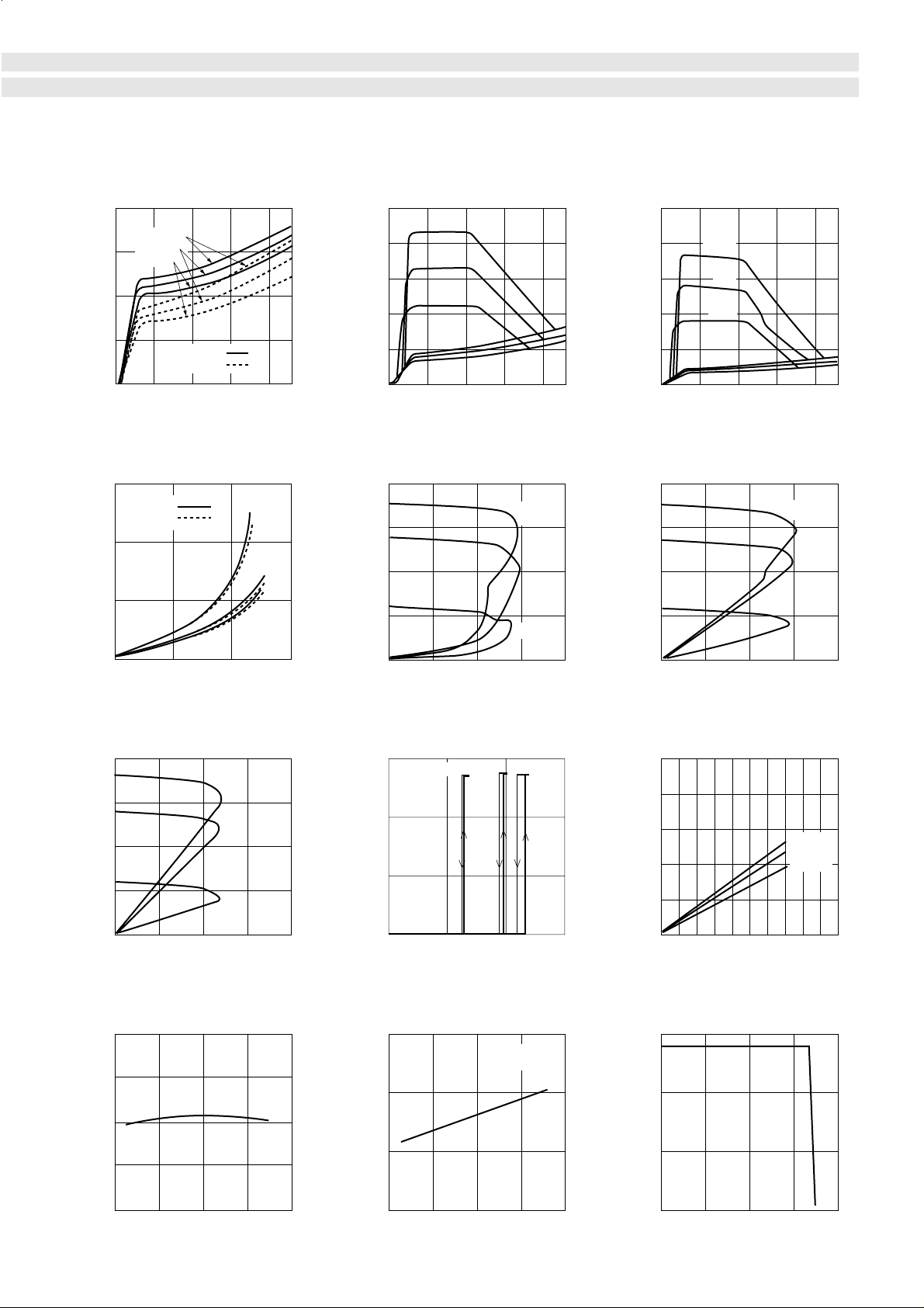
Quiescent Circuit Current (dual circuit)
■
20
Ta
= –40ºC
25ºC
125ºC
(mA)
10
Iq
VO shorted
open
V
O
0
0102030
VB (V)
Circuit Current (single circuit)
IN
4640
50
40
30
(mA)
B
I
20
10
0
0102030
Ta
–40ºC
125ºC
V
IN
=
25ºC
= 0V
V
■
= 0V
V
= 5V
IN
4640
VB (V)
Circuit Current (dual circuit)
■
100
Ta
=
80
60
(mA)
B
I
40
20
0
0102030
–40ºC
125ºC
V
IN
25ºC
= 0V
VB (V)
V
= 5V
IN
4640
Saturation Voltage of Output Transistor
■
1.5
VB= 16V
= 6 V
V
B
1.0
(V)
(sat)
CE
V
0.5
0
012
Ta=
125ºC
25ºC
–40ºC
3
IO (A)
Overcurrent Protection Characteristics (Ta=125ºC)
■
20
V
=
B
18V
14V
6V
(V)
O
V
15
10
5
Overcurrent Protection Characteristics (Ta=–40ºC)
■
20
V
=
B
15
(V)
10
O
V
5
0
012
18V
14V
6V
43
IO (A)
Threshold Characteristics of Input Voltage
■
(V)
V
15
10
O
5
Ta
= 125ºC
25ºC
V
= 14V IO = 1A
B
–40ºC
Overcurrent Protection Characteristics (Ta=25ºC)
■
20
V
=
B
15
(V)
10
O
V
5
0
012
18V
14V
6V
43
IO (A)
Input Terminal Source Current
■
1.0
0.8
0.6
(mA)
IN
I
0.4
0.2
Ta
25ºC
–40ºC
V
= 14V
B
= 125ºC
0
012
IO (A)
Input Terminal Sink Current
■
1.0
(µA)
0.5
INL
I
0
–50 0 50 100
Ta (ºC)
= 14V VIN= 0 V
V
B
150
43
0
012
3
VIN (V)
Saturation Voltage of DIAG Output
■
0.3
V
= 14V
B
= 3mA
I
DIAG
0.2
(V)
DL
V
0.1
0
–50 0 50 100
150
Ta (ºC)
0
02468
VIN (V)
Thermal Protection Characteristics
■
15
10
(V)
O
V
5
0
500 100 150
V
= 14V IO = 10mA
B
Ta (ºC)
10
200
31
 Loading...