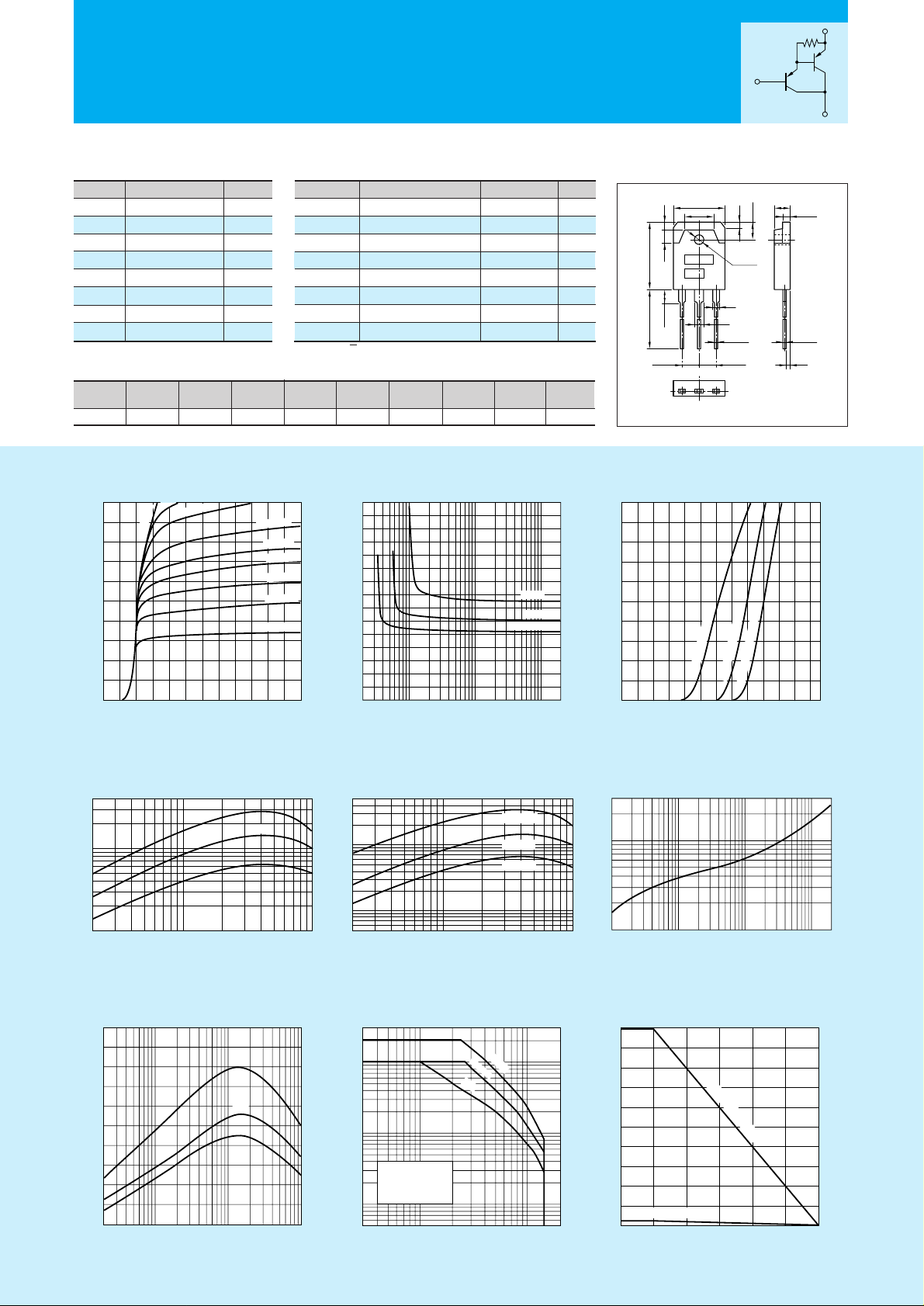
Sanken Electric Co 2SB1560 Datasheet

47
∗hFE Rank O(5000to12000), P(6500to20000), Y(15000to30000)
Darlington 2SB1560
IC–VCE Characteristics
(Typical)
hFE–IC Characteristics
(Typical)
hFE–IC
Temperature Characteristics (Typical)
IC–VBE Temperature Characteristics
(Typical)
VCE(sat)–IB Characteristics
(Typical)
Pc–Ta Derating
0
0
–2
–4
–6
–10
–8
–2 –4 –6
Collector-Emitter Voltage V
CE(V)
Collector Current IC(A)
–10mA
–2.5mA
–2.0mA
–1.5mA
–1.0mA
–1.2mA
–0.8mA
–0.6mA
I
B
=–0.4mA
0
–3
–2
–1
–0.2
–1–0.5 –10–5 –200–100–50
Base Current IB(mA)
Collector-Emitter Saturation Voltage VCE(sat)(V)
–7A
–10A
IC =–5A
0
–10
–8
–6
–2
–4
0 –2.5–2–1
Base-Emittor Voltage VBE(V)
Collector Current IC(A)
(VCE=–4V)
125˚C (Case Temp)
25˚C (Case Temp)
–30˚C (Case Temp)
1,000
10,000
40,000
5,000
–0.2 –0.5 –1 –5 –10
Collector Current I
C(A)
DC Current Gain hFE
(VCE=–4V)
Typ
(VCE=–4V)
–0.2 –1–0.5 –5 –10
500
1000
5000
10000
50000
Collector Current IC(A)
DC Current Gain hFE
125˚C
25˚C
–30˚C
0.1
1
3
0.5
1 5 10 50 100 500 1000 2000
Time t(ms)
Transient Thermal Resistance θj-a(˚C/W)
0.02 0.10.05 0.5 1 5 10
0
40
60
20
100
80
Cut-off Frequency fT(MHZ)
(VCE=–12V)
Emitter Current IE(A)
Typ
10ms
–10 –50–5–3 –100 –200
–0.05
–0.1
–1
–0.5
–10
–30
–5
Collector-Emitter Voltage V
CE(V)
Collector Current IC(A)
DC
100ms
Without Heatsink
Natural Cooling
100
50
3.5
0
0 25 50 75 100 125 150
Ambient Temperature Ta(˚C)
Maximum Power Dissipation PC(W)
With Infinite heatsink
Without Heatsink
Safe Operating Area (Single Pulse)
θj-a
–
t Characteristics
f
T
–
IE Characteristics
(Typical)
Silicon PNP Epitaxial Planar Transistor (Complement to type 2SD2390)
Application : Audio, Series Regulator and General Purpose
Symbol
V
CBO
VCEO
VEBO
IC
IB
PC
Tj
T
stg
2SB1560
–160
–150
–5
–10
–1
100(Tc=25°C)
150
–55 to +150
Unit
V
V
V
A
A
W
°C
°C
■
Absolute maximum ratings
■
Electrical Characteristics
Symbol
I
CBO
IEBO
V(BR)CEO
hFE
VCE(sat)
VBE(sat)
fr
C
OB
2SB1560
–100
max
–100max
–150min
5000min∗
–2.5
max
–3.0max
50typ
230typ
Unit
µ
A
µ
A
V
V
V
MHz
pF
Conditions
V
CB=–160V
V
EB=–5V
I
C=–30mA
V
CE=–4V, IC=–7A
I
C=–7A, IB=–7mA
I
C=–7A, IB=–7mA
V
CE=–12V, IE=2A
V
CB=–10V, f=1MHz
(Ta=25°C)
(Ta=25°C)
■Typical Switching Characteristics (Common Emitter)
V
CC
(V)
–70
R
L
(Ω)
10
I
C
(A)
–7
V
BB2
(V)
5
I
B2
(mA)
7
t
on
(µs)
0.8typ
t
stg
(µs)
3.0typ
t
f
(µs)
1.2typ
I
B1
(mA)
–7
VBB1
(V)
–10
External Dimensions MT-100(TO3P)
15.6
±0.4
9.6
19.9
±0.3
4.0 2.0
5.0
±0.2
1.8
ø3.2
±0.1
2
3
1.05
+0.2
-0.1
20.0min
4.0max
BE
5.45
±0.1
5.45
±0.1
C
4.8
±0.2
0.65
+0.2
-0.1
1.4
2.0
±0.1
a
b
Weight : Approx 6.0g
a. Type No.
b. Lot No.
E
Equivalent circuit
(70Ω)
B
C
 Loading...