

Page 1

SmartMedia™ 32 MByte
Product Manual
®
CORPORATE HEADQUARTERS
140 Caspian Court
Sunnyvale, CA 94089
408-542-0500
FAX: 408-542-0503
URL: http://www.sandisk.com
Page 2

SanDisk® Corporation general policy does not recommend the use of its products in life support applications where in a failure or
malfunction of the product may directly threaten life or injury. Per SanDisk Terms and Conditions of Sale, the user of SanDisk
products in life support applications assumes all risk of such use and indemnifies SanDisk against all damages.
The information in this manual is subject to change without notice.
SanDisk Corporation shall not be liable for technical or editorial errors or omissions contained herein; nor for incidental or
consequential damages resulting from the furnishing, performance, or use of this material.
All parts of the SanDisk documentation are protected by copyright law and all rights are reserved. This documentation may not,
in whole or in part, be copied, photocopied, reproduced, translated, or reduced to any electronic medium or machine readable form
without prior consent, in writing, from SanDisk Corporation.
SanDisk and the SanDisk logo are registered trademarks of SanDisk Corporation. SmartMedia is a trademark of Toshiba
Corporation.
Product names mentioned herein are for identification purposes only and may be trademarks and/or registered trademarks of
their respective companies.
© 2001 SanDisk Corporation. All rights reserved.
SanDisk products are covered or licensed under one or more of the following U.S. Patent Nos. 5,070,032; 5,095,344; 5,168,465;
5,172,338; 5,198,380; 5,200,959; 5,268,318; 5,268,870; 5,272,669; 5,418,752; 5,602,987. Other U.S. and foreign patents
awarded and pending.
Lit. No. 80-36-00169 Rev. 1.1 6/01 Printed in U.S.A.
Revision History
• Revision 1—initial release.
• Revision 1.1—corrected typo on memory cell array; changed from 128K to 64K, page 5.
2
SmartMedia 32 MByte Product Manual Rev. 1.1 © 2001 SANDISK CORPORATION
Page 3

SmartMedia 32 MByte Product Manual
Table of Contents
1.0 Description..............................................................................................................................5
1.1 Features...................................................................................................................................................5
2.0 Timing Diagrams ..................................................................................................................12
3.0 Pin Functions ........................................................................................................................20
3.1 Pin Descriptions...................................................................................................................................21
3.2 Schematic Cell Layout and Address Assignment...........................................................................22
3.3 Operation Mode: Logic and Command Tables...............................................................................23
4.0 Device Operation ..................................................................................................................25
4.1 Read Mode (1)......................................................................................................................................25
4.2 Read Mode (2)......................................................................................................................................26
4.3 Read Mode (3)......................................................................................................................................27
4.4 Sequential Read (1) (2) (3) ..................................................................................................................28
4.5 Status Read...........................................................................................................................................28
4.6 Auto Page Program.............................................................................................................................30
4.7 Auto Block Erase .................................................................................................................................30
4.8 Reset ......................................................................................................................................................31
4.9 ID Read .................................................................................................................................................32
5.0 Application Notes and Comments ........................................................................................33
5.1 Prohibition of Unspecified Commands............................................................................................33
5.2 Pointer Control for 00H, 01H and 50H.............................................................................................33
5.3 Acceptable Commands After Serial Input Command 80H...........................................................34
5.4 Status Read During a Read Operation .............................................................................................35
5.5 Auto-Programming Failure ...............................................................................................................35
R/B
5.6
5.7 Status After Power-on ........................................................................................................................36
5.8 Power-on/off Sequence......................................................................................................................36
5.9 Note Regarding the
5.10 When Four Address Cycles are Input ..............................................................................................38
5.11 Several Programming Cycles on the Same Page (Partial Page Program)....................................39
5.12 Note Regarding the
5.13 Invalid Blocks (Bad Blocks)................................................................................................................40
5.14 Failure Phenomena for Program and Erase Operations................................................................41
5.15 Bad Block Test Flow............................................................................................................................ 42
: Termination for the Ready/Busy Pin (
WP
Signal.......................................................................................................37
Signal.........................................................................................................39
RE
R/B
)........................................................................36
6.0 Handling Precautions............................................................................................................43
7.0 Package Dimensions .............................................................................................................44
7.1 SmartMedia Card Dimensions..........................................................................................................44
SmartMedia 32 MByte Product Manual Rev.1.1 © 2001 SANDISK CORPORATION 3
Page 4

SmartMedia 32 MByte Product Manual
Table of Contents (continued)
Ordering Information and Technical Support................................................................................45
Ordering Information.....................................................................................................................47
SmartMedia Card...........................................................................................................................................47
Technical Support Services............................................................................................................48
Direct SanDisk Technical Support...............................................................................................................48
SanDisk Worldwide Web Site...................................................................................................................... 48
SanDisk Worldwide Sales Offices.................................................................................................51
Limited Warranty...........................................................................................................................53
4
SmartMedia 32 MByte Product Manual Rev. 1.1 © 2001 SANDISK CORPORATION
Page 5

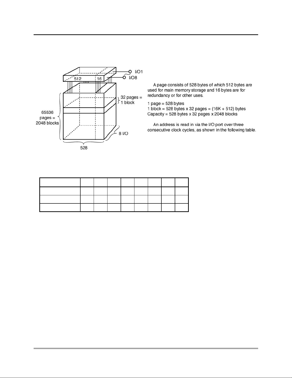
1.0 Description
SmartMedia 32 MByte Product Manual
The SanDisk SmartMedia Card (SDSM-32-101-01) is a 3.3-V 256-Mbit (276,824,064) NAND Electrically
Erasable and Programmable Read-Only Memory (NAND E
2
PROM) device, organized as 528 bytes X 32
pages X 2048 blocks. This device has a 528-byte static register which allows program and read data to be
transferred between the register and the memory cell array in 528-byte increments. The Erase operation is
implemented in a single block unit (16 Kbytes + 512 bytes: 528 bytes X 32 pages).
The SanDisk SmartMedia Card is a serial-type memory device which uses the I/O pins for both address
and data input and output as well as for command inputs. The Erase and Program operations are
automatically executed making the device ideal for applications such as solid-state file storage, voice
recording, image storage for digital cameras and other devices which require high-density non-volatile
memory data storage. The data stored in the SmartMedia Card needs to comply with the data format
standardized by the SSFDC Forum in order to maintain compatibility with other SmartMedia
TM
systems.
1.1 Features
• Organization
- Memory cell array 528 × 64K × 8
- Data Register 528 × 8
- Page size 528 bytes
- Block size (16K + 512) bytes
•Modes
- Read, Reset, Auto Page Program
- Auto Block Erase, Status Read
• Mode control
- Serial Input/Output
- Command control
• Complies with the SmartMedia Electrical Specification and Data Format Specification issued by
SSFDC Forum (SmartMedia Card).
• Power Supply— V
• Access time
- Cell array to register 10 µs max
- Serial Read Cycle 50 ns min
• Operating current
- Read (50 ns cycle) 10 mA typ.
- Program (avg.) 10 mA typ.
- Erase (avg.) 10 mA typ.
- Standby 100 µA max
•Package
- SDSM-32-101-01: SmartMedia Card (Weight: 1.8 g. typical)
= 3.3 V ± 0.3 V
CC
SmartMedia 32 MByte Product Manual Rev.1.1 © 2001 SANDISK CORPORATION 5
Page 6

SmartMedia 32 MByte Product Manual
SDSM-32-101-01
123456
CLE ALE WE WP I/O2I/O1 I/O3 I/O4V
ss
22 21 20 19 18 17 16 15 14 13 12
CE RE R/B OP LVD I/O8 I/O7 I/O6 I/O5 V
V
CC
7891011
VssV
ss
I/O1 to 8
CC
CE
WE
RE
CLE
ALE
WP
R/B
OP
LVD
V
CC
V
SS
PIN NAMES
I/O Port
Chip Enable
Write Enable
Read Enable
Command Latch Enable
Address Latch Enable
Write Protect
Ready/Busy
Option Pin (GND Input)
Low Voltage Detect
Power Supply
Ground
Figure 1-1 SDSM-32-101-01 SmartMedia Card Pin Assignments (Top View)
Figure 1-2 Block Diagram
6
SmartMedia 32 MByte Product Manual Rev. 1.1 © 2001 SANDISK CORPORATION
Page 7
SmartMedia 32 MByte Product Manual
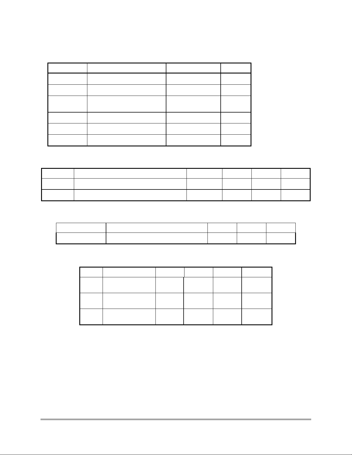
Table 1-1 Absolute Maximum Ratings
Symbol Rating Value Unit
V
CC
V
V
I/O
T
SOLDER
T
STG
T
OPR
Power Supply Voltage
IN
Input Voltage
Input /Output Voltage
−0.6 to 4.6
−0.6 to 4.6
0.6 V to V
(≤4.6 V)
+ 0.3 V
CC
Soldering Temperature (10s) - °C
Storage Temperature
−20 to 65
Operating Temperature 0 to 55 °C
V
V
V
°C
Table 1-2 Capacitance *(Ta = 25°C, f = 1 MHz)
Symbol Parameter Condition Min. Max. Unit
Input
Output
VIN = 0 V
= 0 V
V
OUT
C
C
OUT
IN
* This parameter is periodically sampled and is not tested for every device.
(1)
Table 1-3 Valid Blocks
Symbol Parameter MIN MAX Unit
N
VB
(1) The SmartMedia Card occasionally contains unusable blocks. Refer to section 5.13.
Number of Valid Blocks 2008 2048 Blocks
10 pF
10 pF
Table 1-4 Recommended DC Operating Conditions
Symbol Parameter Min. Typ. Max. Unit
V
CC
V
IH
V
IL
Power Supply
Voltage
High Level Input
Voltage
Low Level Input
Voltage
* −2V (pulse width ≤ 20 ns)
SmartMedia 32 MByte Product Manual Rev.1.1 © 2001 SANDISK CORPORATION 7
3.0 3.3 3.6 V
2.0
−0.3*
V
+ 0.3
CC
0.8 V
V
Page 8
SmartMedia 32 MByte Product Manual
Table 1-5 DC Characteristics
(Ta = 0° to 55° C, V
Symbol Parameter Condition Min. Typ. Max. Unit
= 3.3V ± 0.3V)
CC
I
I
I
I
I
I
I
I
IOL (
I
IL
I
LO
CCO1
CCO3
CCO4
CCO5
CCO7
CCO8
CCS1
CCS2
V
OH
V
OL
R/B
Input Leakage Current
Output Leakage Current
Operating Current
(Serial Read)
Operating Current
(Command Input)
Operating Current
(Data Input)
Operating Current
(Address Input)
Programming Current
Erasing Current
Standby Current
Standby Current
High Level Output Voltage
Low Level Output Voltage
)
Output current of
R/B
pin
= 0V to V
V
IN
V
= 0.4V to V
OUT
CE
= VIL, I
t
cycle
t
cycle
t
cycle
t
cycle
CE
CE
= VCC − 0.2V
IOH = −400 µA
IOL = 2.1 mA
V
OL
CC
CC
= 0 mA,
OUT
= 50 ns
= 50 ns
= 50 ns
= 50 ns
= V
IH
= 0.4V
±10 µA
±10 µA
10 30 mA
10 30 mA
10 30 mA
10 30 mA
10 30 mA
10 30 mA
2.4
8
1mA
100
0.4 V
µA
V
mA
8
SmartMedia 32 MByte Product Manual Rev. 1.1 © 2001 SANDISK CORPORATION
Page 9

SmartMedia 32 MByte Product Manual
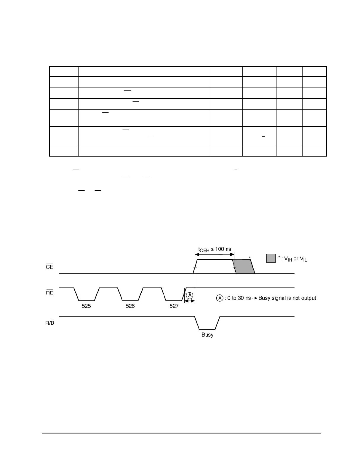
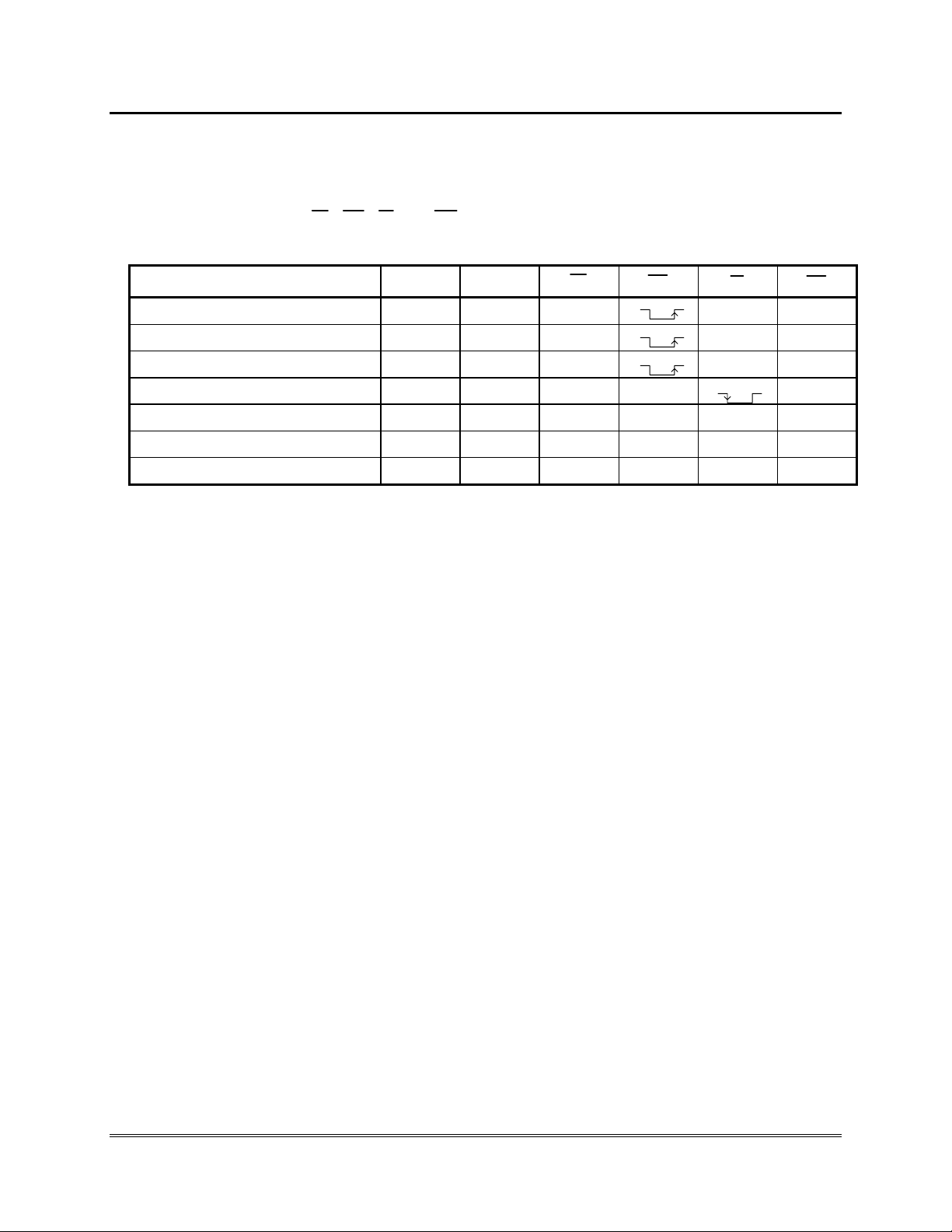
Table 1-6 AC Characteristics and Recommended Operating Conditions
(Ta = 0° to 55° C, V
Symbol Parameter Min. Max. Unit Notes
= 3.3V ± 0.3V)
CC
t
CLS
t
CLH
t
CS
t
CH
t
WP
t
ALS
t
ALH
t
DS
t
DH
t
WC
t
WH
t
WW
t
RR
t
RP
t
RC
t
REA
t
CEH
t
REAID
t
OH
t
RHZ
t
CHZ
t
REH
t
t
RSTO
t
CSTO
t
RHW
t
WHC
t
WHR
t
AR1
t
CR
CLE Setup Time 0
CLE Hold Time 10
Setup Time
CE
Hold Time
CE
0
10
Write Pulse Width 25
ALE Setup Time 0
ALE Hold Time 10
Data Setup Time 20
Data Hold Time 10
Write Cycle Time 50
High Hold Time
WE
High to WE Low
WP
Ready to RE Falling Edge
15
100
20
Read Pulse Width 35
Read Cycle Time 50
Access Time (Serial Data Access)
RE
High Time for Last Address in Serial Read Cycle
CE
Access Time (ID Read)
RE
100
Data Output Hold Time 10
High to Output High Impedance
RE
High to Output High Impedance
CE
High Hold Time
RE
IR
Output High impedance to RE Rising Edge
Access Time (Status Read)
RE
Access Time (Status Read)
CE
High to WE Low
RE
High to CE Low
WE
WE
High to RE Low
ALE Low to RE Low (ID Read)
Low to RE Low (ID Read)
CE
15
0
0
30
30
100
100
35 ns
35 ns
30 ns
20 ns
35 ns
45 ns
ns
ns
ns
ns
ns
ns
ns
ns
ns
ns
ns
ns
ns
ns
ns
ns (3)
ns
ns
ns
ns
ns
ns
ns
ns
SmartMedia 32 MByte Product Manual Rev.1.1 © 2001 SANDISK CORPORATION 9
Page 10
SmartMedia 32 MByte Product Manual
Table 1-6 AC Characteristics and Recommended Operating Conditions (continued)
Symbol Parameter Min. Max. Unit Notes
Memory Cell Array to Starting Address
ALE Low to RE Low (Read Cycle)
RE
(When interrupted by
Device Reset Time (Read/Program/Erase)
t
t
t
t
t
t
R
WB
AR2
RB
CRY
RST
Notes: (1) Transition time (t
High to Ready time depends on the pull-up resistor tied to the
(2)
CE
(3) If the delay between
will stop.
If the
to CE delay is less than 30 ns, the device will not re-enter Busy state.
RE
AC Test Conditions:
Input level: 2.4V/0.4V
Input Comparison Level: 1.5V/1.5V
Output Data Comparison Level: 1.5V/1.5V
Output Load: 1 TTL + C
High to Busy
WE
Last Clock Rising Edge to Busy
(in Sequential Read)
High to Ready
CE
in Read Mode)
CE
)
= 5 ns.
T
and CE is less than 200 ns and t
RE
(100 pF)
L
50
pin. (Refer to section 5.6.)
R/B
is greater than or equal to 100 ns, reading
CEH
10
200 ns
200 ns
600 +
t
(
)
R/B
r
6/10/500
µs
ns
ns (2)
µs
10
Figure 1-3
SmartMedia 32 MByte Product Manual Rev. 1.1 © 2001 SANDISK CORPORATION
Page 11
SmartMedia 32 MByte Product Manual
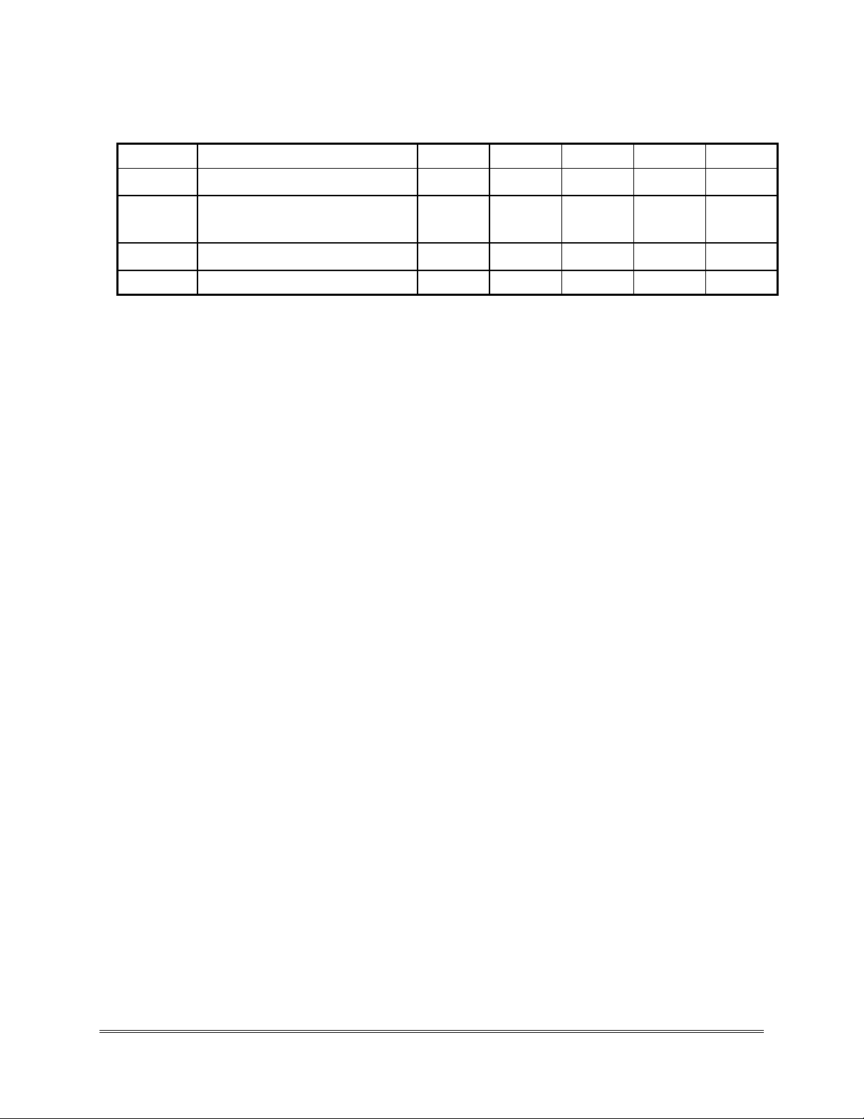
Table 1-7 Programming and Erasing Characteristics
(Ta = 0° to 55° C, V
Symbol Parameter Min. Typ. Max. Unit Notes
= 3.3V ± 0.3V)
CC
t
PROG
N
t
BERASE
P/E Number of Program/Erase Cycles 300,000 (2)
Notes: (1) Refer to section 5.11.
(2) Refer to section 5.14.
Average Programming Time 200 1000
Number of Programming Cycles on
Same Page
Block Erasing Time 3 20 ms
µs
(1)
10
SmartMedia 32 MByte Product Manual Rev.1.1 © 2001 SANDISK CORPORATION 11
Page 12
SmartMedia 32 MByte Product Manual
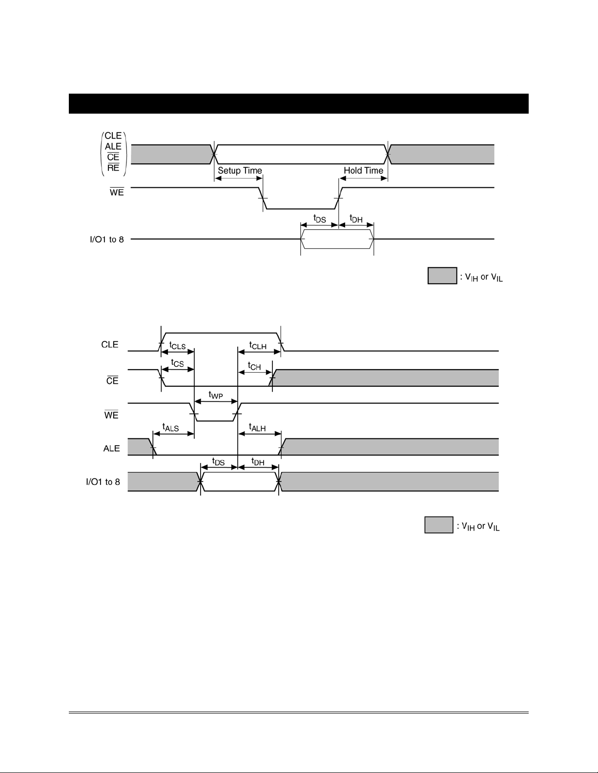
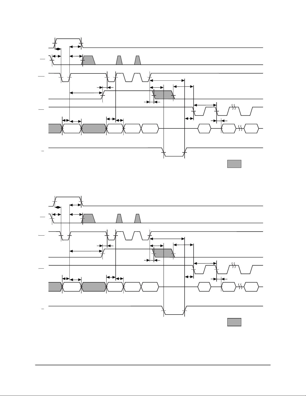
2.0 Timing Diagrams
Figure 2-1 Latch Timing Diagram for Command/Address/Data
12
Figure 2-2 Command Input Cycle Timing Diagram
SmartMedia 32 MByte Product Manual Rev. 1.1 © 2001 SANDISK CORPORATION
Page 13
SmartMedia 32 MByte Product Manual
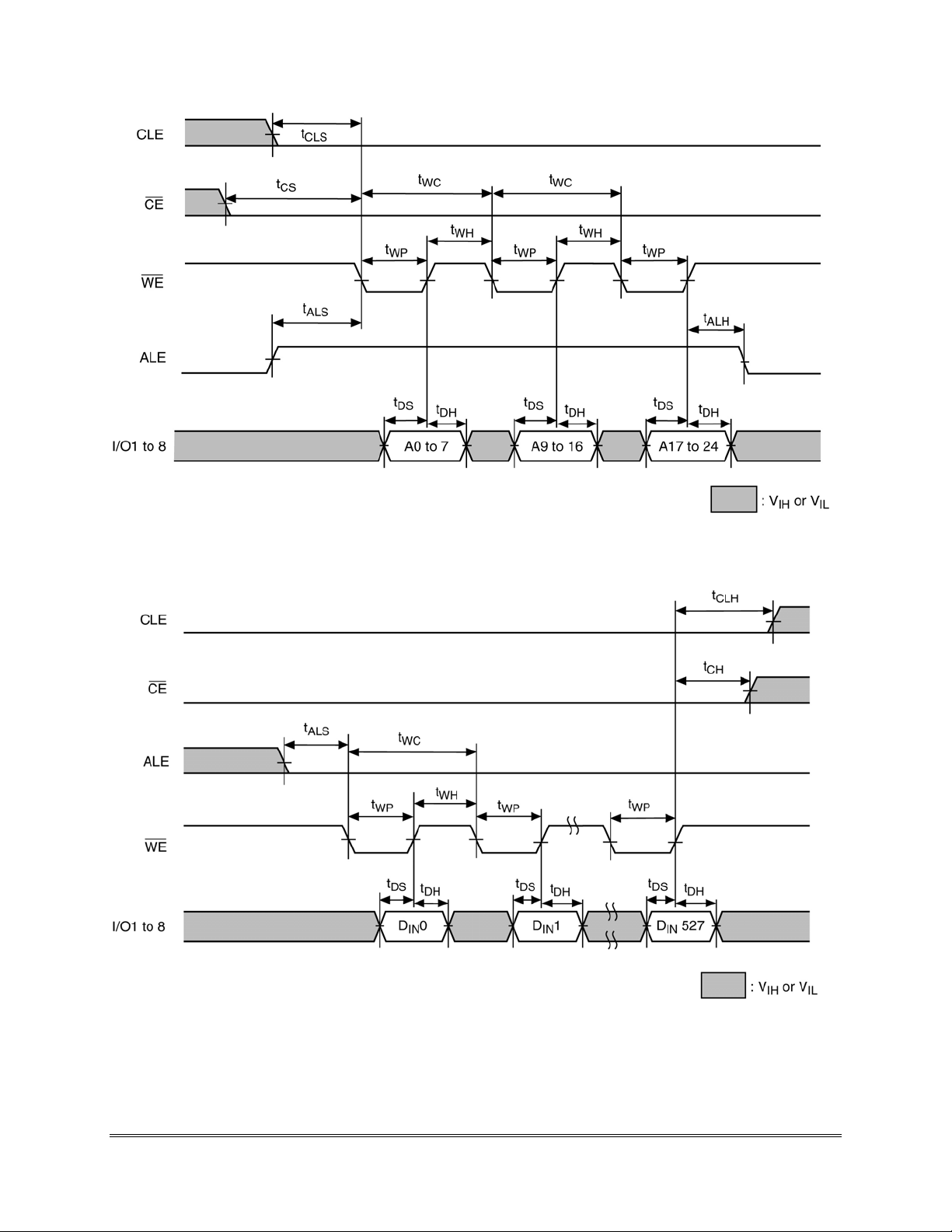
Figure 2-3 Address Input Cycle Timing Diagram
Figure 2-4 Data Input Cycle Timing Diagram
SmartMedia 32 MByte Product Manual Rev.1.1 © 2001 SANDISK CORPORATION 13
Page 14
SmartMedia 32 MByte Product Manual
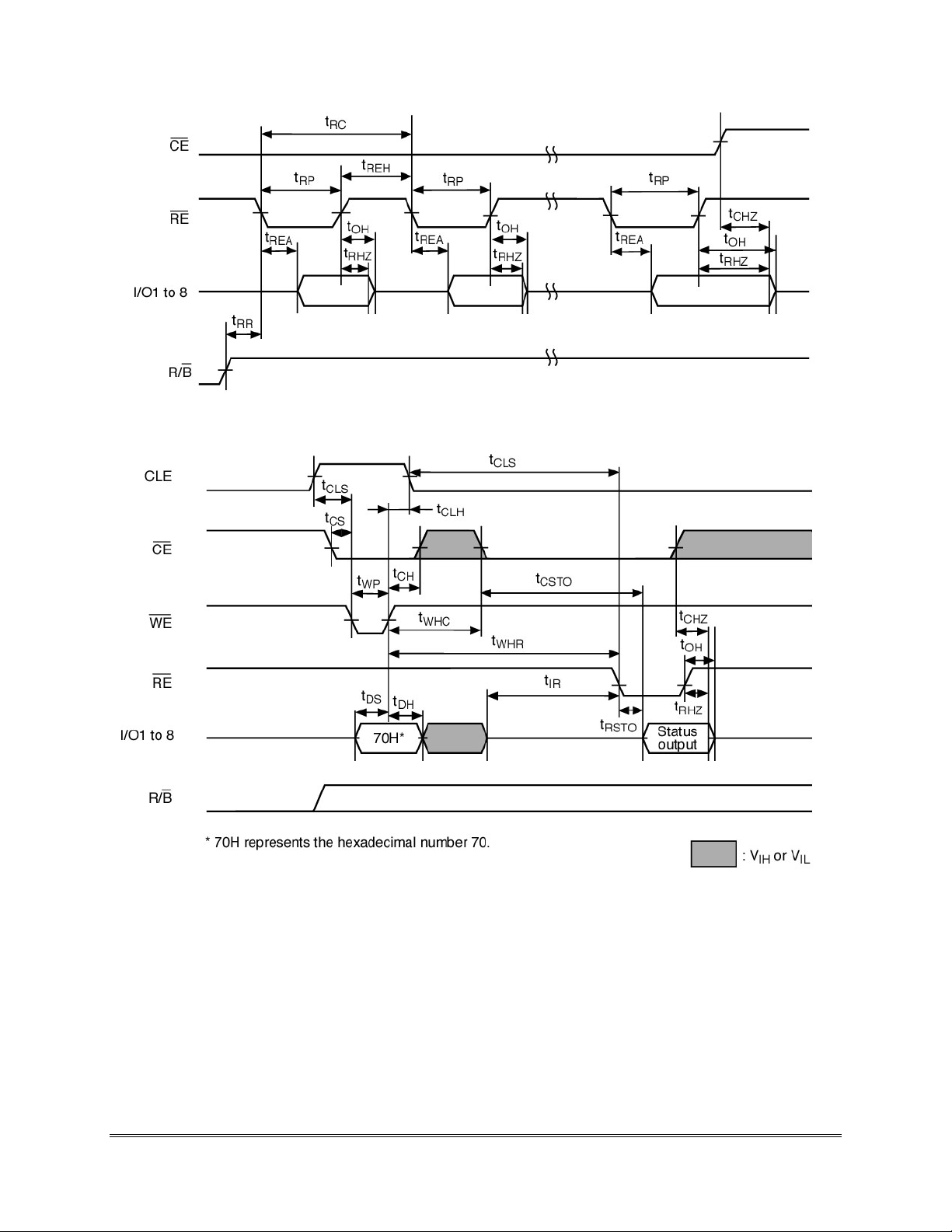
Figure 2-5 Serial Read Cycle Timing Diagram
14
Figure 2-6 Status Read Cycle Timing Diagram
SmartMedia 32 MByte Product Manual Rev. 1.1 © 2001 SANDISK CORPORATION
Page 15
SmartMedia 32 MByte Product Manual
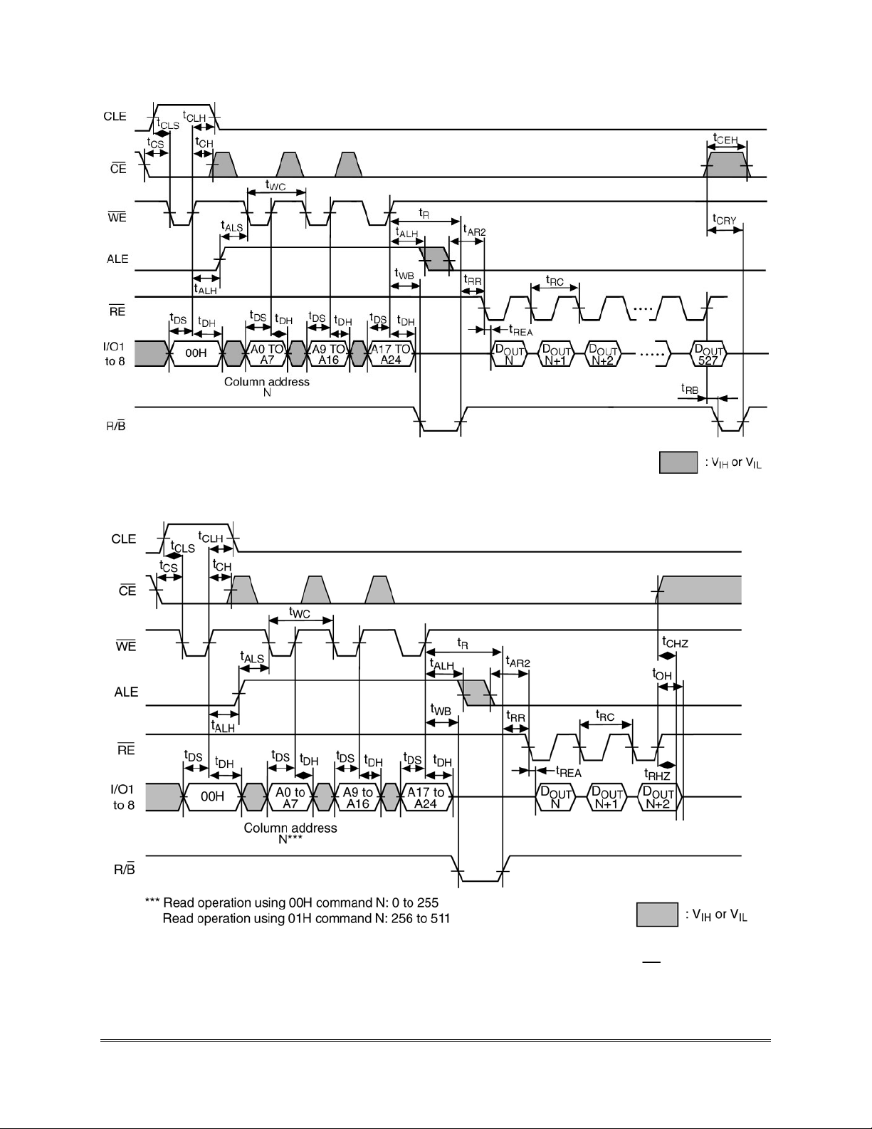
Figure 2-7 Read Cycle (1) Timing Diagram
Figure 2-8 Read Cycle (1) Timing Diagram When Interrupted by
SmartMedia 32 MByte Product Manual Rev.1.1 © 2001 SANDISK CORPORATION 15
CE
Page 16
SmartMedia 32 MByte Product Manual
t
CLE
CE
WE
ALE
t
CS
t
CLS
CLH
t
CH
t
ALH
t
ALS
t
ALH
t
WB
t
R
t
AR 2
t
RC
RE
I/O1
to 8
R/B
CLE
CE
WE
ALE
t
DS
t
DH
01H
t
DS
t
DH
A0 to
A7
Column address
N
A9 to
A16
A17 to
A24
t
D
REA
OUT
t
RR
D
OUT
256 + N 256 + N + 1 527
: V
D
OUT
IH
or V
IL
Figure 2-9 Read Cycle (2) Timing Diagram
t
CLH
t
CLS
t
CS
t
CH
t
R
t
AR 2
t
RC
t
ALH
t
ALS
t
ALH
t
WB
RE
I/O1
to 8
R/B
16
t
DS
t
DH
50H
t
DS
t
DH
A0 to
A7
Column address
N
A9 to
A16
A17 to
A24
t
D
REA
OUT
t
RR
D
OUT
512 + N 512 + N + 1 527
: V
D
OUT
IH
or V
IL
Figure 2-10 Read Cycle (3) Timing Diagram
SmartMedia 32 MByte Product Manual Rev. 1.1 © 2001 SANDISK CORPORATION
Page 17
SmartMedia 32 MByte Product Manual
Figure 2-11 Sequential Read (1) Timing Diagram
Figure 2-12 Sequential Read (2) Timing Diagram
SmartMedia 32 MByte Product Manual Rev.1.1 © 2001 SANDISK CORPORATION 17
Page 18

SmartMedia 32 MByte Product Manual
Figure 2-13 Sequential Read (3) Timing Diagram
18
Figure 2-14 Auto Program Operation Timing Diagram
SmartMedia 32 MByte Product Manual Rev. 1.1 © 2001 SANDISK CORPORATION
Page 19

SmartMedia 32 MByte Product Manual
Figure 2-15 Auto Block Erase Timing Diagram
Figure 2-16 ID Read Operation Timing Diagram
SmartMedia 32 MByte Product Manual Rev.1.1 © 2001 SANDISK CORPORATION 19
Page 20

SmartMedia 32 MByte Product Manual
3.0 Pin Functions
The device is a serial access memory which utilizes time-sharing input of address information. The device
pinouts are configured as shown in Figure 3-1.
SDSM-32-101-01
123456
CLE ALE WE WP I/O2I/O1 I/O3 I/O4V
ss
22 21 20 19 18 17 16 15 14 13 12
CE RE R/B OP LVD I/O8 I/O7 I/O6 I/O5 V
V
CC
7891011
VssV
Figure 3-1 SmartMedia Card Pinout
ss
I/O1 to 8
CC
CE
WE
RE
CLE
ALE
WP
R/B
OP
LVD
V
CC
V
SS
PIN NAMES
I/O Port
Chip Enable
Write Enable
Read Enable
Command Latch Enable
Address Latch Enable
Write Protect
Ready/Busy
Option Pin (GND Input)
Low Voltage Detect
Power Supply
Ground
20
SmartMedia 32 MByte Product Manual Rev. 1.1 © 2001 SANDISK CORPORATION
Page 21

SmartMedia 32 MByte Product Manual
3.1 Pin Descriptions
Command Latch Enable: CLE
The CLE input signal is used to control loading of the operation mode command into the internal
command register. The command is latched into the command register from the I/O port on the rising
edge of the
Address Latch Enable: ALE
The ALE signal is used to control loading of either address information or input data into the internal
address/data register. Address information is latched on the rising edge of
Low, input data is latched.
signal while CLE is High.
WE
if ALE is High. If ALE is
WE
Chip Enable:
The device goes into a low-power Standby Mode when CE goes High during a Read operation. The
signal is ignored when the device is in the Busy state (
operation, and will not enter Standby Mode even if the
CE
= L), such as during a Program or Erase
R/B
CE
input goes High. The
CE
signal must stay
CE
Low during the Read Mode Busy state to ensure that memory array data is correctly transferred to the
data register.
Write Enable:
WE
The
Read Enable:
The RE signal controls serial data output. Data output will be valid when RE goes low after t
WE
signal is used to control the acquisition of data from the I/O port.
RE
REA
. The
internal column address counter is also incremented (Address = Address + l) on this falling edge.
I/O Port: I/OI to 8
The I/O1 to 8 pins are used as ports for transferring address, command and input/output data to and
from the device.
Write Protect:
WP
The WP signal is used to protect the device from accidental programming or erasing. The internal
voltage regulator is reset when
WP
is Low. This signal is usually used for protecting the data during the
power-on/off sequence when input signals are invalid.
Ready/Busy:
R/B
The
state (
R/B
R/B
output signal is used to indicate the operating condition of the device. The
R/B
signal is in Busy
= L) during the Program, Erase and Read operations and will return to Ready state (
R/B
= H)
after completion of the operation. The output buffer for this signal is an open drain.
Option Pin: OP
This pin has to be connected to GND.
Low Voltage Detect: LVD (SmartMedia Card only)
The LVD signal is used to detect the power supply voltage level.
SmartMedia 32 MByte Product Manual Rev.1.1 © 2001 SANDISK CORPORATION 21
Page 22
SmartMedia 32 MByte Product Manual
3.2 Schematic Cell Layout and Address Assignment
The Program operation works on page units while the Erase operation works on block units.
Figure 3-2 Schematic Cell Layout
Table 3-1 Addressing
I/O2 I/O3 I/O4 I/O5 I/O6 I/O7 I/O8
I/O1
First cycle A0 A1 A2 A3 A4 A5 A6 A7 A9 to A24: Page address
Second cycle A9 A10 A11 A12 A13 A14 A15 A16 (A14 to A24: Block address
Third cycle A17 A18 A19 A20 A21 A22 A23 A24 A9 to A13: NAND address in block)
* : A8 is automatically set to Low or High by a 00H command or a 01H command.
A0 to A7: Column address
22
SmartMedia 32 MByte Product Manual Rev. 1.1 © 2001 SANDISK CORPORATION
Page 23
SmartMedia 32 MByte Product Manual
3.3 Operation Mode: Logic and Command Tables
The operation modes such as Program, Erase, Read and Reset are controlled by the eleven different
command operations shown in Table 3-3. Address input, command input and data input/output are
controlled by the CLE, ALE,
Table 3-2 Logic Table
CE
,
,
WE
RE
and
WP
signals, as shown in Table 3-2.
CLE ALE
Command Input H L L H
Data Input L L L H
Address input L H L H
Serial Data Output L L L H
During Programming (Busy)
During Erasing (Busy)
Program, Erase Inhibit
H: VIH, L: VIL, *: VIH or V
IL
*****
*****
*****
CE
WE
RE
WP
*
*
*
*
H
H
L
SmartMedia 32 MByte Product Manual Rev.1.1 © 2001 SANDISK CORPORATION 23
Page 24
SmartMedia 32 MByte Product Manual
Table 3-3 Command Table (HEX)
First Cycle
Second
Cycle
Acceptable while Busy
Serial Data Input 80
Read Mode (1) 00
Read Mode (2) 01
Read Mode (3) 50
Reset FF
Auto Program 10
Auto Block Erase 60 D0
Status Read 70
ID Read 90
√
√
Table 3-4 Read Mode Operation States
CLE ALE
Output select
Output Deselect
Standby
H: VIH, L: VIL, *: VIH or V
24
IL
L L L H L Data output Active
L L L H H High impedance Active
LLHH
SmartMedia 32 MByte Product Manual Rev. 1.1 © 2001 SANDISK CORPORATION
CE
WE RE
I/O1 to I/O8 Power
*
High impedance Standby
Page 25
SmartMedia 32 MByte Product Manual
4.0 Device Operation
4.1 Read Mode (1)
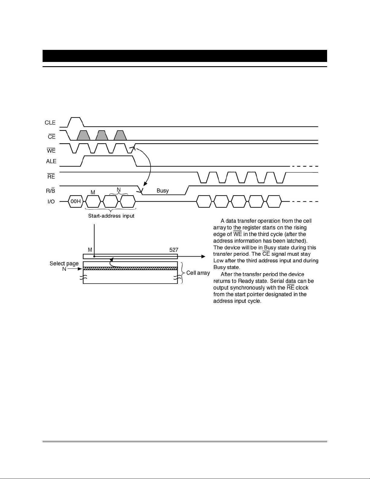
Read Mode (l) is set when an 00H command is issued to the Command register. Refer to Figure 4-1 below
for timing details and the block diagram.
Figure 4-1 Read Mode (1) Operation
SmartMedia 32 MByte Product Manual Rev.1.1 © 2001 SANDISK CORPORATION 25
Page 26

SmartMedia 32 MByte Product Manual
4.2 Read Mode (2)
Figure 4-2 Read Mode (2) Operation
26
SmartMedia 32 MByte Product Manual Rev. 1.1 © 2001 SANDISK CORPORATION
Page 27

SmartMedia 32 MByte Product Manual
4.3 Read Mode (3)
Read Mode (3) has the same timing as Read Modes (1) and (2) but is used to access information in the
extra 16-byte redundancy area of the page. Therefore, the start pointer is set to a value between byte 512
and byte 527.
Figure 4-3 Read Mode (3) Operation
SmartMedia 32 MByte Product Manual Rev.1.1 © 2001 SANDISK CORPORATION 27
Page 28

SmartMedia 32 MByte Product Manual
4.4 Sequential Read (1) (2) (3)
This mode, Sequential Read (1) (2) (3), allows the sequential reading of pages without additional address
input.
Figure 4-4 Sequential Read (1) (2) (3) Operation
Sequential Read modes (1) and (2) output the contents of addresses 0 to 527 as shown above, while
Sequential Read mode (3) outputs the contents of the redundant address locations only. When the pointer
reaches the last address, the device continues to output the data from column address 0 (Read Modes (1)
and (2)) or column address 512 (Read Mode (3)) of the next page on the next
RE
clock signal.
4.5 Status Read
The device automatically implements the execution and verification of the Program and Erase operations.
The Status Read function is used to monitor the Ready/Busy status of the device, determine the result
(pass /fail) of a Program or Erase operation, and determine whether the device is in Suspend or Protect
mode. The device status is output via the I/O port on the
resulting information is outlined in Table 4-1.
Table 4-1 Status Output Table
Status Output
I/O1 Pass/Fail Pass: 0 Fail: 1
I/O2 Not Used 0
I/O3 Not Used 0
I/O4 Not Used 0
I/O5 Not Used 0
clock after a 70H command input. The
RE
The Pass/Fail status on I/O1 is only
valid when the device is in the Ready
state.
28
I/O6 Not Used 0
I/O7 Ready/Busy Ready: 1 Busy: 0
I/O8
Write Protect
Protect: 0 Not Protected: 1
SmartMedia 32 MByte Product Manual Rev. 1.1 © 2001 SANDISK CORPORATION
Page 29

SmartMedia 32 MByte Product Manual
An application example with multiple devices is shown in Figure 4-5.
Figure 4-5 Application Example with Multiple Devices
Figure 4-6 Status Read Timing Application Example
System Design Note: If the
pin signals from multiple devices are wired together as shown in the
R/B
Figure 4-5, the Status Read function can be used to determine the status of each individual device.
SmartMedia 32 MByte Product Manual Rev.1.1 © 2001 SANDISK CORPORATION 29
Page 30

SmartMedia 32 MByte Product Manual
4.6 Auto Page Program
The SmartMedia Card carries out an Automatic Page Program operation when it receives a 10H Program
command after the address and data have been input. The sequence of command, address and data input
is shown below.
Figure 4-7 Auto Page Program Operation
4.7 Auto Block Erase
The Auto Block Erase operation starts on the rising edge of
which follows the Erase Setup command 60H. This two-cycle process for Erase operations acts as an extra
layer of protection from accidental erasure of data due to external noise. The device automatically
executes the Erase and Verify operations.
Figure 4-8 Auto Block Erase
WE
after the Erase Start command D0H
30
SmartMedia 32 MByte Product Manual Rev. 1.1 © 2001 SANDISK CORPORATION
Page 31

SmartMedia 32 MByte Product Manual
4.8 Reset
The Reset mode stops all operations. For example, in the case of a Program or Erase operation the
internally generated voltage is discharged to 0 volts and the device enters Wait state. The address and
data registers are set as follows after a Reset:
• Address register: All “0”
• Data register: All “1”
• Operation Mode: Wait state
Figure 4-9 through 4-13 show the response to an FFH Reset command input during the various device
operations.
Figure 4-9 When a Reset Command (FFH) is Input During Programming
Figure 4-10 When a Reset Command (FFH) is Input During Erasing
Figure 4-11 When a Reset Command (FFH) is Input During a Read Operation
Figure 4-12 When a Status Read Command (70H) is Input After a Reset
SmartMedia 32 MByte Product Manual Rev.1.1 © 2001 SANDISK CORPORATION 31
Page 32

SmartMedia 32 MByte Product Manual
Figure 4-13 When Two or More Reset Commands are Input in Succession
4.9 ID Read
The SmartMedia Card contain ID codes which identify the device type and the manufacturer. The ID
codes can be read out under the following timing conditions:
Figure 4-14 ID Read Timing
Table 4-2 Code Table
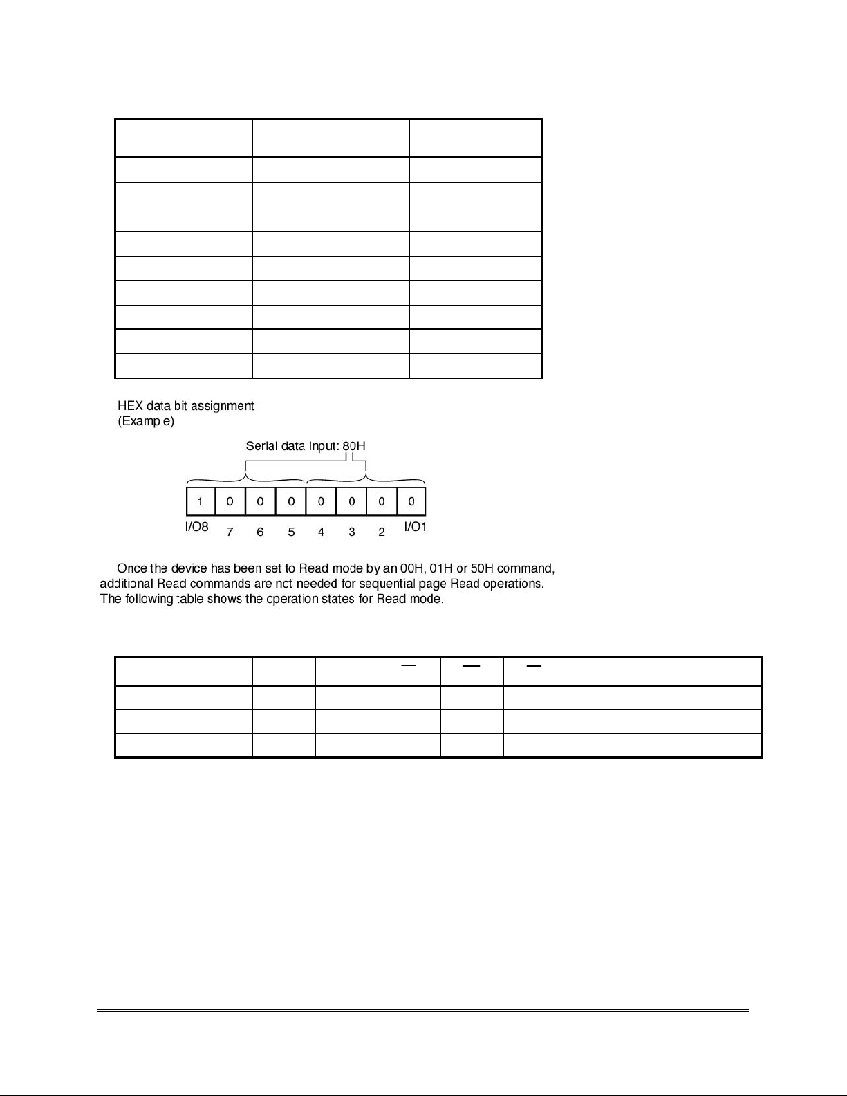
I/O8 I/O7 I/O6 I/O5 I/O4 I/O3 I/O2 I/O1 Hex Data
Maker code 10011000 98H
Device code 01110101 75H
32
SmartMedia 32 MByte Product Manual Rev. 1.1 © 2001 SANDISK CORPORATION
Page 33

SmartMedia 32 MByte Product Manual
5.0 Application Notes and Comments
5.1 Prohibition of Unspecified Commands
The operation commands are listed in Table 3-3. Input of a command other than those specified in Table
3-3 is prohibited. Stored data may be corrupted if an unknown command is entered during the command
cycle.
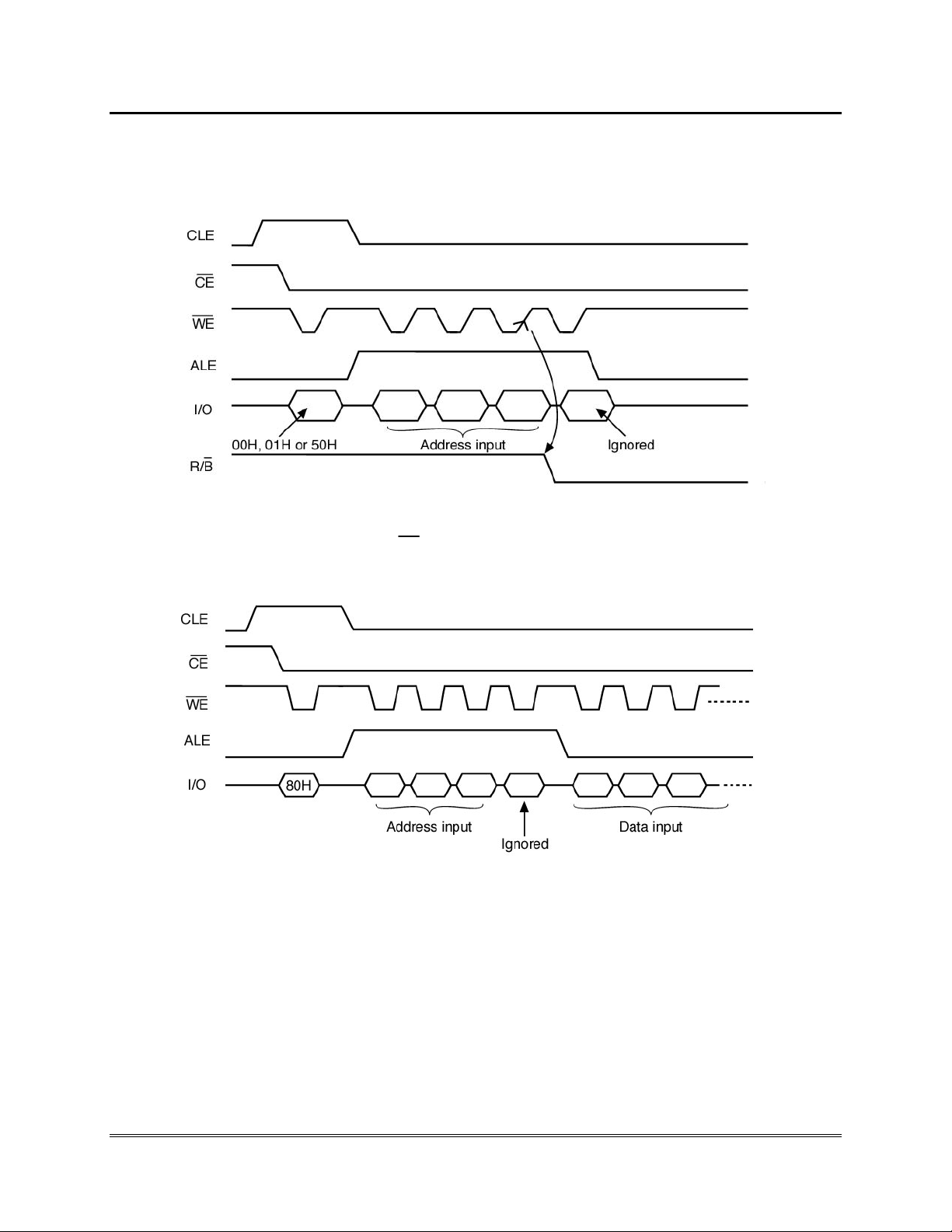
5.2 Pointer Control for 00H, 01H and 50H
The device has three Read modes which set the destination of the pointer. Table 5-1 shows the destination
of the pointer, and Figure 5-1 is a block diagram of their operations.
Table 5-1 Pointer Destination
Read Mode Command Pointer
(1) 00H 0 to 255
(2) 01H 256 to 511
(3) 50H 512 to 527
Figure 5-1 Pointer Control
The pointer is set to region A by the 00H command, to region B by the 01H command and to region C by
the 50H command. For example, the 00H command must be input to set the pointer back to region A
when the pointer is pointing to region C.
SmartMedia 32 MByte Product Manual Rev.1.1 © 2001 SANDISK CORPORATION 33
Page 34

SmartMedia 32 MByte Product Manual
Figure 5-2 Example of How to Set Pointer
5.3 Acceptable Commands After Serial Input Command 80H
Once the Serial Input command 80H has been input, do not input any command other than the Program
Execution command 10H or the Reset command FFH.
Figure 5-3 Serial Input Command
34
SmartMedia 32 MByte Product Manual Rev. 1.1 © 2001 SANDISK CORPORATION
Page 35

SmartMedia 32 MByte Product Manual
5.4 Status Read During a Read Operation
Figure 5-4 Status Read During a Read Operation
The device status can be read out by inputting the Status Read command 70H in Read mode. Once the
device has been set to Status Read mode by a 70H command, the device will not return to Read mode.
Therefore, a Status Read during a Read operation is prohibited.
However, when the Read command 00H is input during [A], Status mode is reset and the device returns
to Read mode. In this case, data output starts automatically from address N and address input is
unnecessary.
5.5 Auto-Programming Failure
Figure 5-5 Auto-programming Failure
SmartMedia 32 MByte Product Manual Rev.1.1 © 2001 SANDISK CORPORATION 35
Page 36
SmartMedia 32 MByte Product Manual
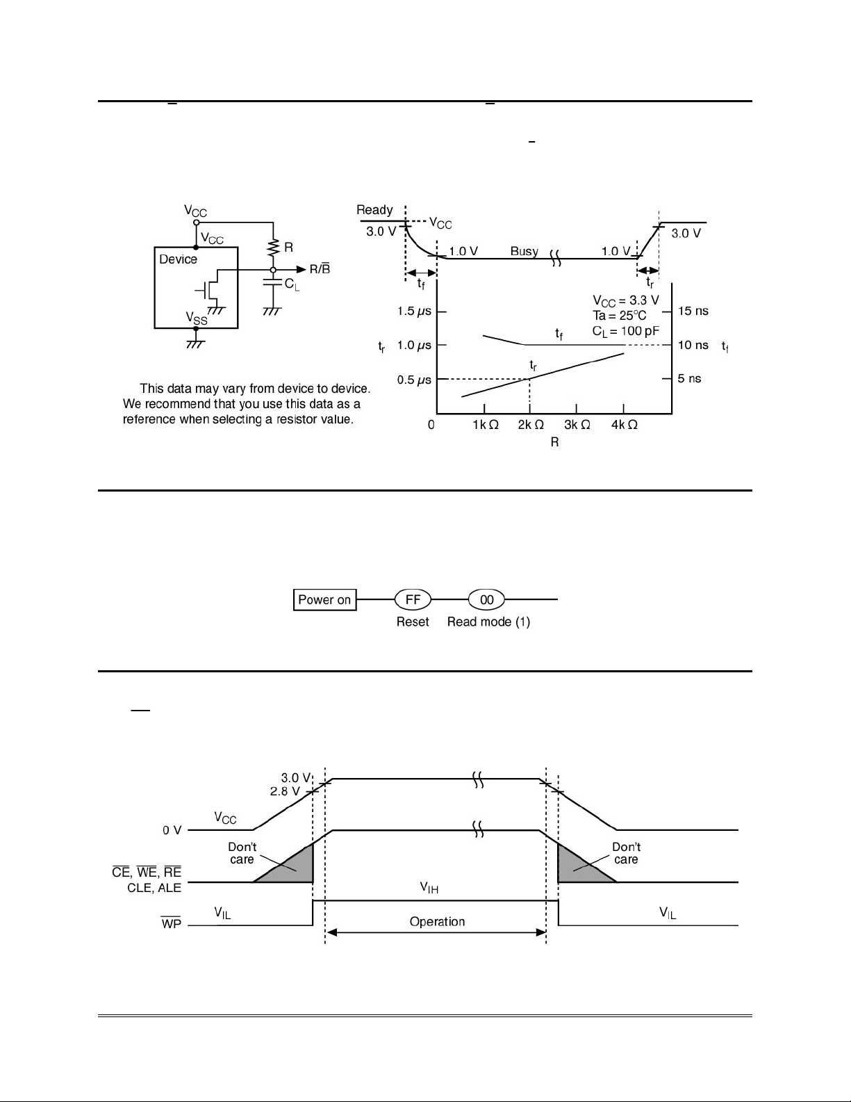
5.6
A pull-up resistor needs to be used for termination because the
circuit.
R/B
: Termination for the Ready/Busy Pin (
Figure 5-6 Termination of the Ready/Busy Pin
R/B
)
5.7 Status After Power-on
buffer consists of an open drain
R/B
Although the device is set to Read mode after power-on, the following sequence is necessary because
some input signals may not be stable at power-on.
Figure 5-7 Status After Power-on
5.8 Power-on/off Sequence
WP
The
sequence is necessary:
signal is useful for protecting against data corruption at power-on/off. The following timing
36
Figure 5-8 Power-on/off Sequence
SmartMedia 32 MByte Product Manual Rev. 1.1 © 2001 SANDISK CORPORATION
Page 37

SmartMedia 32 MByte Product Manual
5.9 Note Regarding the
The Erase and Program operations are automatically reset when
enabled and disabled as shown in the following figures:
WP
Signal
Figure 5-9 Enable Programming
WP
goes Low. The operations are
Figure 5-10 Disable Programming
Figure 5-11 Enable Erasing
Figure 5-12 Disable Erasing
SmartMedia 32 MByte Product Manual Rev.1.1 © 2001 SANDISK CORPORATION 37
Page 38
SmartMedia 32 MByte Product Manual
5.10 When Four Address Cycles are Input
Although the SmartMedia Card may read in a fourth address, it is ignored inside the device.
Figure 5-13 Read Operation
The internal Read Operation starts when
Figure 5-14 Program Operation
goes High in the address cycle.
WE
38
SmartMedia 32 MByte Product Manual Rev. 1.1 © 2001 SANDISK CORPORATION
Page 39

SmartMedia 32 MByte Product Manual
5.11 Several Programming Cycles on the Same Page (Partial Page Program)
A page can be divided into up to 10 segments. Each segment can be programmed individually as follows:
Note: The input data for unprogrammed or previously programmed page segments must be “1” (i.e. the inputs for
all page bytes outside the segment which is to be programmed should be set to all “1”).
Figure 5-15 Partial Page Program
5.12 Note Regarding the
The internal column address counter is incremented synchronously with the RE clock in Read Mode.
Therefore, once the device has been set to Read Mode by an 00H, 01H or 50H command, the internal
column address counter is incremented by the
clock input pulses start before the address input, and the pointer reaches the last column address, an
RE
internal read operation (array to register) will occur and the device will enter Busy state. (Refer to the
figure below.) Hence, the
Figure 5-16 Internal Read Operation (Array to Register)
RE
Signal
RE
clock independently of the address input timing. If the
RE
clock input must start after the address input.
SmartMedia 32 MByte Product Manual Rev.1.1 © 2001 SANDISK CORPORATION 39
Page 40

SmartMedia 32 MByte Product Manual
k
k
5.13 Invalid Blocks (Bad Blocks)
The SmartMedia Card occasionally contains unusable blocks. Therefore, the following issues must be
recognized:
• Check to see whether the device has any bad blocks after installation into the system. Do not try
to access bad blocks. A bad block does not affect the performance of good blocks because it is
isolated from the bit line by the Select gate. The number of valid blocks is as follows:
Table 5-2 Number of Valid Blocks
Minimum Maximum Unit
Valid (Good)
Blocks
Figure 5-19 shows the flow for bad block testing.
2008 2048 Block
Figure 5-17 Bad Blocks in Array
Bad Bloc
Bad Bloc
40
SmartMedia 32 MByte Product Manual Rev. 1.1 © 2001 SANDISK CORPORATION
Page 41

SmartMedia 32 MByte Product Manual
5.14 Failure Phenomena for Program and Erase Operations
The device may fail during a Program or Erase operation. The following possible failure modes should be
considered when implementing a highly reliable system.
Table 5-3 Failure Modes
Failure Mode Detection and Counter Measure Sequence
Block Erase Failure
Page Programming Failure
Single
Bit*
Programming Failure
“1 to 0”
Status Read after Erase → Block Replacement
Status Read after Program → Block Replacement
(1) Block Verify after Program → Retry
(2) ECC
* : (1) or (2)
• ECC: Error Correction Code—Hamming code , etc. Example: 1-bit correction and 2-bit
detection.
• Block Replacement
Figure 5-18 Program Fail Block Replacement
• Erase Block Replacement—When an error occurs in an Erase operation, prevent future accesses to
this bad block (again by creating a table within the system or by using another appropriate
scheme).
SmartMedia 32 MByte Product Manual Rev.1.1 © 2001 SANDISK CORPORATION 41
Page 42

SmartMedia 32 MByte Product Manual
5.15 Bad Block Test Flow
Test Start
Block No. = 1
Blank Check
Fail
Bad Block
B No. = B No. + 1
B No. > 2048
Yes
Block No. = 1
32-Page
C-Patt Prog
Pass
Read (00H)
Pass
Block Erase
Pass
32-Page
C-Patt Prog
Pass
Read (00H)
Pass
Block Erase
Pass
No
Fail
Fail
Fail
Fail
Fail
Fail
C : Checkerboard pattern
C : Inverted checkerboard pattern
Blank check : 1 Block Read (FFH)
B No. = B No. + 1
Bad
Block
B No. = 2048
No
Yes
42
B No. = 2048
Yes
Test End
No
Figure 5-19 Bad Block Test Flow
SmartMedia 32 MByte Product Manual Rev. 1.1 © 2001 SANDISK CORPORATION
Page 43

SmartMedia 32 MByte Product Manual
6.0 Handling Precautions
The following precautions should be observed when handling the SanDisk SmartMedia Card:
(1) Avoid using the SmartMedia Card when the battery is low.
(2) When writing to the card, wait for the operation to complete before removing the card.
(3) The card is designed to fit easily into the system one way only. Do not force it into the slot.
(4) Do not bend the card.
(5) Do not subject the card to sudden impact.
(6) Avoid touching the connectors so as to avoid damage from static electricity. This card should be kept
in the antistatic film case when not in use.
SmartMedia 32 MByte Product Manual Rev.1.1 © 2001 SANDISK CORPORATION 43
Page 44

SmartMedia 32 MByte Product Manual
7.0 Package Dimensions
7.1 SmartMedia Card Dimensions
The SanDisk SmartMedia Card dimensions are shown below in Figure 7-1.
44
Figure 7-1 SmartMedia Card Dimensions
SmartMedia 32 MByte Product Manual Rev. 1.1 © 2001 SANDISK CORPORATION
Page 45

Ordering Information
and
Technical Support
SmartMedia 32 MByte Product Manual Rev.1.1 © 2001 SANDISK CORPORATION 45
Page 46

This page has been left blank intentionally.
46
SmartMedia 32 MByte Product Manual Rev. 1.1 © 2001 SANDISK CORPORATION
Page 47

Ordering Information and Technical Support
Ordering Information
To order SanDisk products directly from SanDisk, call 408-542-0595.
SmartMedia Card
Model SDSM-32-101-01 32.0 MB
SmartMedia 32 MByte Product Manual Rev.1.1 © 2001 SANDISK CORPORATION 47
Page 48

Ordering Information and Technical Support
Technical Support Services
Direct SanDisk Technical Support
Call SanDisk Applications Engineering at 408-542-0405 for technical support.
SanDisk Worldwide Web Site
Internet users can obtain technical support and product information along with SanDisk news and much
more from the SanDisk Worldwide Web Site, 24 hours a day, seven days a week. The SanDisk Worldwide
Web Site is frequently updated. Visit this site often to obtain the most up-to-date information on SanDisk
products and applications. The SanDisk Web Site URL is http://www.sandisk.com.
48
SmartMedia 32 MByte Product Manual Rev. 1.1 © 2001 SANDISK CORPORATION
Page 49

SanDisk Sales Offices
SmartMedia 32 MByte Product Manual Rev.1.1 © 2001 SANDISK CORPORATION 49
Page 50

This page has been left blank intentionally.
50
SmartMedia 32 MByte Product Manual Rev. 1.1 © 2001 SANDISK CORPORATION
Page 51

SanDisk Worldwide Sales Offices
SanDisk Worldwide Sales Offices
Americas
SanDisk Corporate Headquarters
140 Caspian Court
Sunnyvale, CA 94089-9820
408-542-0500
FAX 408-542-0503
http://www.sandisk.com
Sales Offices
Western Region USA
408-542-0730
FAX 408-542-0403
Eastern Region USA & Canada
603-882-0888
FAX 603-882-2201
Central & Southern Region USA
614-760-3700
FAX 614-760-3701
Latin & South America
407-667-4880
FAX 407-667-4834
Europe
SanDisk GmbH
Karlsruher Str. 2C
D-30519 Hannover, Germany
49-511-8759185
FAX 49-511-8759187
SanDisk Northern Europe
Videroegaten 3 B
S-16440 Kista
Sweden
46-(0)8-75084-63
FAX 46-(0)8-75084-26
SanDisk Central Europe
Rudolf-Diesel-Str. 3
40822 Mettmann
Germany
49-(0)2104-953433
FAX 49-(0)2104-953434
Japan
SanDisk K.K.
8F Nisso Bldg. 15
2-17-19 Shin-Yokohama, Kohoku-ku
Yokohama 222-0033, Japan
81-45-474-0181
FAX 81-45-474-0371
Asia/Pacific Rim
89 Queensway, Lippo Center
Tower II, Suite 4104
Admiralty, Hong Kong
852-2712-0501
FAX 852-2712-9385
To order SanDisk products directly from SanDisk,
call 408-542-0595.
SmartMedia 32 MByte Product Manual Rev. 1.1 © 2001 SANDISK CORPORATION
51
Page 52

This page has been left blank intentionally.
52
SmartMedia 32 MByte Product Manual Rev. 1.1 © 2001 SANDISK CORPORATION
Page 53

Limited Warranty
Limited Warranty
I. WARRANTY STATEMENT
SanDisk warrants its products to be free of any defects in materials or workmanship that would prevent them from
functioning properly for one year from the date of purchase. This express warranty is extended by SanDisk
Corporation.
II. GENERAL PROVISIONS
This warranty sets forth the full extent of SanDisk’s responsibilities regarding the SanDisk SmartMedia Card. In
satisfaction of its obligations hereunder, SanDisk, at its sole option, will either repair, replace or refund the purchase
price of the product.
NOTWITHSTANDING ANYTHING ELSE IN THIS LIMITED WARRANTY OR OTHERWISE, THE EXPRESS
WARRANTIES AND OBLIGATIONS OF SELLER AS SET FORTH IN THIS LIMITED WARRANTY, ARE IN LIEU
OF, AND BUYER EXPRESSLY WAIVES ALL OTHER OBLIGATIONS, GUARANTIES AND WARRANTIES OF ANY
KIND, WHETHER EXPRESS OR IMPLIED, INCLUDING WITHOUT LIMITATION, ANY IMPLIED WARRANTY
OF MERCHANTABILITY OR FITNESS FOR A PARTICULAR PURPOSE OR INFRINGEMENT, TOGETHER WITH
ANY LIABILITY OF SELLER UNDER ANY CONTRACT, NEGLIGENCE, STRICT LIABILITY OR OTHER LEGAL
OR EQUITABLE THEORY FOR LOSS OF USE, REVENUE, OR PROFIT OR OTHER INCIDENTAL OR
CONSEQUENTIAL DAMAGES, INCLUDING WITHOUT LIMITATION PHYSICAL INJURY OR DEATH,
PROPERTY DAMAGE, LOST DATA, OR COSTS OF PROCUREMENT OF SUBSTITUTE GOODS, TECHNOLOGY
OR SERVICES. IN NO EVENT SHALL THE SELLER BE LIABLE FOR DAMAGES IN EXCESS OF THE PURCHASE
PRICE OF THE PRODUCT, ARISING OUT OF THE USE OR INABILITY TO USE SUCH PRODUCT, TO THE FULL
EXTENT SUCH MAY BE DISCLAIMED BY LAW.
SanDisk’s products are not warranted to operate without failure. Accordingly, in any use of products in life support
systems or other applications where failure could cause injury or loss of life, the products should only be
incorporated in systems designed with appropriate redundancy, fault tolerant or back-up features.
III. WHAT THIS WARRANTY COVERS
For products found to be defective within one year of purchase, SanDisk will have the option of repairing or
replacing the defective product, if the following conditions are met:
A. The defective product is returned to SanDisk for failure analysis as soon as possible after the failure occurs.
B. An incident card filled out by the user, explaining the conditions of usage and the nature of the failure,
accompanies each returned defective product.
C. No evidence is found of abuse or operation of products not in accordance with the published specifications,
or of exceeding storage or maximum ratings or operating conditions.
All failing products returned to SanDisk under the provisions of this limited warranty shall be tested to the product’s
functional and performance specifications. Upon confirmation of failure, each product will be analyzed, by whatever
means necessary, to determine the root cause of failure. If the root cause of failure is found to be not covered by the
above provisions, then the product will be returned to the customer with a report indicating why the failure was not
covered under the warranty.
This warranty does not cover defects, malfunctions, performance failures or damages to the unit resulting from use in
other than its normal and customary manner, misuse, accident or neglect; or improper alterations or repairs.
SanDisk reserves the right to repair or replace, at its discretion, any product returned by its customers, even if such
product is not covered under warranty, but is under no obligation to do so.
SanDisk may, at its discretion, ship repaired or rebuilt products identified in the same way as new products,
provided such cards meet or exceed the same published specifications as new products. Concurrently, SanDisk also
reserves the right to market any products, whether new, repaired, or rebuilt, under different specifications and
product designations if such products do not meet the original product’s specifications.
SmartMedia 32 MByte Product Manual Rev. 1.1 © 2001 SANDISK CORPORATION
53
Page 54

Limited Warranty
IV. RECEIVING WARRANTY SERVICE
According to SanDisk’s warranty procedure, defective product should be returned only with prior authorization
from SanDisk Corporation. Please contact SanDisk’s Customer Service department at 408-542-0595 with the following
information: product model number and description, nature of defect, conditions of use, proof of purchase and
purchase date. If approved, SanDisk will issue a Return Material Authorization or Product Repair Authorization
number. Ship the defective product to:
SanDisk Corporation
Attn: RMA Returns
(Reference RMA or PRA #)
140 Caspian Court
Sunnyvale, CA 94089
V. STATE LAW RIGHTS
SOME STATES DO NOT ALLOW THE EXCLUSION OR LIMITATION OF INCIDENTAL OR CONSEQUENTIAL
DAMAGES, OR LIMITATION ON HOW LONG AN IMPLIED WARRANTY LASTS, SO THE ABOVE
LIMITATIONS OR EXCLUSIONS MAY NOT APPLY TO YOU. This warranty gives you specific rights and you may
also have other rights that vary from state to state.
54
SmartMedia 32 MByte Product Manual Rev. 1.1 © 2001 SANDISK CORPORATION
 Loading...