

Page 1

®
C
ORPORATE HEADQUARTERS
140 Caspian Court
Sunnyvale, CA 94089-1000
408-542-0500
FAX: 408-542-0503
URL: http://www.sandisk.com
Page 2

SanDisk® Corporation general policy does not recommend the use of its products in life support applications where in a failure
or malfunction of the product may directly threaten life or injury. Per SanDisk Terms and Conditions of Sale, the user of SanDisk
products in life support applications assumes all risk of such use and indemnifies SanDisk against all damages.
The information in this manual is subject to change without notice.
SanDisk Corporation shall not be li able for technical or editorial errors or omiss ions contained herein; nor for inc idental or
consequential damages resulting from the furnishing, performance, or use of this material.
All parts of the SanDisk M ultiMediaCard documentation are protected by copyright law and all rights are reserved. This
documentation may not, in whole or in part, be copied, photocopied, reproduced, translated, or reduced to any electronic
medium or machine-readable form without prior consent, in writing, from SanDisk Corporation.
SanDisk and the SanDisk logo are regi stered tradem arks of SanDisk Corporation.
Product names mentioned herein are for identification purposes onl y and may be trademarks and/or registered t rademarks of
their respective companies.
© 2002 SanDisk Corporation. All rights reserved.
SanDisk products are covered or licensed under one or more of the followi ng U.S . Pat ent Nos. 5,070,032; 5, 095,344; 5,168,465;
5,172,338; 5,198,380; 5,200,959; 5,268,318; 5, 268, 870; 5,272,669; 5,418,752; 5, 602,987. Other U.S. and foreign patents
awarded and pending.
Lit. No. 80-13-00089 Rev. 5.1 8/2002 Printed in U.S.A.
Revision His tory
• Revisions dated before 1/98—Initial release and general changes.
• Revision dated 1/98—General editorial changes, manual reorganized, technical changes to reflect support of MultiMediaCard
Specification version 1.3, new timing diagrams added. Pin 6 definition changed in SPI mode from SPI select to VSS2 (supply
voltage ground).
• Revision dated 4/98—Changes reflect support of MultiMediaC ard S pe cificatio n ve rsio n 1.4, update d timing for Multiple W rite
with no Busy, updated SPI command class definition, added Erro r Protection section, changed operating temperature
specification to -25° to 85°C.
• Revision dated 4/28/98—Updated C_SIZE and C_SIZE_MULT field definitions.
• Revision 1 dated 4/99—Added 32 MB MultiMediaCard, general technical and editorial changes, added power up section.
• Revision 2 dated 4/2000—Changed mechanical specification drawing, clarified s ystem performance specifications, editorial
changes.
• Revision 3 dated 7/2001—Manual reformatted, new capacities and specifications added. Changes reflect support of
MultiMediaCard Specification, version 2.11.
•
Revision 4 dated 11/2001—Manual reformatted, minor editorial changes.
Specification, version 2.2.
•
Revision 5 dated 6/2002—Minor editorial and technical changes.
•
Revision 5.1 dated 7/2002—Minor editorial and technical changes.
Changes reflect support of MultiMediaCard
ii MultiMediaCard Product Manual, Rev. 5.1 © 2002 SANDISK CORPORATION
Page 3

Table of Contents
1. Introduction to the MultiMediaCard.............................................................................................................1-1
1.1. Scope........................................................................................................................................... 1-2
1.2. Product Models............................................................................................................................ 1-2
1.3. System Features...........................................................................................................................1-2
1.4. MultiMediaCard Standard ...........................................................................................................1-3
1.5. Functional Description.................................................................................................... .............1-3
1.5.1. Flash Technology Independence.........................................................................................1-4
1.5.2. Defect and Error Management ...........................................................................................1-4
1.5.3. Endurance..........................................................................................................................1-4
1.5.4. Automatic Sleep Mode.................................................................................................... ...1-5
1.5.5. Hot Insertion......................................................................................................................1-5
1.5.6. MultiMediaCard Mode.......................................................................................................1-5
1.5.6.1. MultiMediaCard Standard Compliance..............................................................1-5
1.5.6.2. Negotiating Operation Conditions.....................................................................1-5
1.5.7. Card Acquisition and Identification....................................................................................1-5
1.5.7.1. Card Status........................................................................................................ 1-6
1.5.7.2. Memory Array Partitioning................................................................................1-6
1.5.7.3. Read and Write Operations................................................................................1-8
1.5.7.4. Data Protection in the Flash Card ......................................................................1-9
1.5.7.5. Erase................................................................................................................. 1-9
1.5.7.6. Write Protection ................................................................................................1-9
1.5.7.7. Copy Bit............................................................................................................1-9
1.5.7.8. The CSD Register..............................................................................................1-9
1.5.8. SPI Mode...........................................................................................................................1-10
1.5.8.1. Negotiating Operating Conditions .....................................................................1-10
1.5.8.2. Card Acquisition and Identification...................................................................1-10
1.5.8.3. Card Status........................................................................................................ 1-10
1.5.8.4. Memory Array Partitioning................................................................................1-10
1.5.8.5. Read and Write Operations................................................................................1-11
1.5.8.6. Data Transfer Rate............................................................................................1-11
1.5.8.7. Data Protection in the MultiMediaCard.............................................................1-11
1.5.8.8. Erase................................................................................................................. 1-11
1.5.8.9. Write Protection ................................................................................................1-11
2. Product Specifications ..................................................................................................................................2-1
2.1. System Environmental Specifications...........................................................................................2-1
2.2. Typical System Power Requirements............................................................................................2-1
2.3. System Performance.....................................................................................................................2-2
2.4. System Reliability and Maintenance............................................................................................. 2-2
2.5. Physical Specifications................................................................................................................. 2-2
3. MultiMediaCard Interface Description .........................................................................................................3-1
3.1. Physical Description ....................................................................................................................3-1
3.1.1. Pin Assignments in MultiMediaCard Mode........................................................................3-1
3.1.2. Pin Assignments in SPI Mode ............................................................................................3-1
3.2. MultiMediaCard Bus Topology.................................................................................................... 3-2
3.2.1. Power Protection................................................................................................................ 3-3
3.3. SPI Bus Topology........................................................................................................................3-3
3.3.1. Power Protection................................................................................................................ 3-4
3.4. Electrical Interface.......................................................................................................................3-4
3.4.1. Power-up............................................................................................................................3-4
3.4.2. Bus Operating Conditions..................................................................................................3-6
i MultiMediaCard Product Manual, Rev. 5.1 © 2002 SANDISK CORPORATION
Page 4

Table of Contents
3.4.3. Bus Signal Levels...............................................................................................................3-7
3.4.4. Open-Drain Mode Bus Signal Level...................................................................................3-7
3.4.5. Push-pull Mode Bus Signal Level.......................................................................................3-7
3.4.6. Bus Timing........................................................................................................................3-8
3.5. MultiMediaCard Registers...........................................................................................................3-9
3.5.1. Operating Conditions Register (OCR)................................................................................3-9
3.5.2. Card Identification (CID) Register .....................................................................................3-10
3.5.3. Card Specific Data (CSD) Register.....................................................................................3-11
3.5.4. Status Register ...................................................................................................................3-17
3.5.5. Relative Card Address (RCA) Register...............................................................................3-19
3.5.6. MultiMediaCard Registers in SPI Mode.............................................................................3-19
3.6. File System Format......................................................................................................................3-19
4. MultiMediaCard Protocol Description..........................................................................................................4-1
4.1. Card Identification Mode.............................................................................................................4-2
4.1.1. Reset..................................................................................................................................4-2
4.1.2. Operating Voltage Range Validation..................................................................................4-3
4.1.3. Card Identification Process.................................................................................................4-3
4.2. Data Transfer Mode .....................................................................................................................4-4
4.2.1. Data Read Format..............................................................................................................4-5
4.2.2. Data Write Format............................................................................................................. 4-6
4.2.3. CSD Programming.............................................................................................................4-7
4.2.4. Erase..................................................................................................................................4-7
4.2.5. Write Protect Management.................................................................................................4-7
4.2.6. Card Lock/Unlock Operation..............................................................................................4-8
4.2.6.1. Setting the Password..........................................................................................4-9
4.2.6.2. Reset the Password ............................................................................................ 4-9
4.2.6.3. Locking a Card..................................................................................................4-9
4.2.6.4. Unlocking the Card ........................................................................................... 4-10
4.2.6.5. Forcing Erase....................................................................................................4-10
4.3. Clock Control..............................................................................................................................4-11
4.4. Cyclic Redundancy Codes (CRC).................................................................................................4-11
4.5. Error Conditions..........................................................................................................................4-13
4.5.1. CRC and Illegal Command................................................................................................4-13
4.5.2. Read, Write and Erase Time-out Conditions.......................................................................4-13
4.6. Commands...................................................................................................................................4-14
4.6.1. Command Types................................................................................................................4-14
4.6.2. Command Format .............................................................................................................. 4-14
4.6.3. Command Classes..............................................................................................................4-14
4.6.4. Detailed Command Description..........................................................................................4-15
4.7. Card State Transition Tables........................................................................................................4-18
4.8. Responses....................................................................................................................................4-20
4.8.1. Data Response....................................................................................................................4-21
4.9. Timings.......................................................................................................................................4-21
4.9.1. Command and Response....................................................................................................4-22
4.9.2. Data Read..........................................................................................................................4-23
4.9.3. Data Write.........................................................................................................................4-23
4.9.4. Timing Values...................................................................................................................4-25
ii MultiMediaCard Product Manual, Rev. 5.1 © 2002 SANDISK CORPORATION
Page 5

Table of Contents
5. SPI Mode .....................................................................................................................................................5-1
5.1. SPI Interface Concept..................................................................................................................5-1
5.2. SPI Bus Topology........................................................................................................................5-1
5.3. MultiMediaCard Registers in SPI Mode.......................................................................................5-3
5.4. SPI Bus Protocol..........................................................................................................................5-3
5.4.1. Mode Selection ..................................................................................................................5-3
5.4.2. Bus Transfer Protection......................................................................................................5-4
5.4.3. Data Read..........................................................................................................................5-4
5.4.4. Data Write.........................................................................................................................5-6
5.4.5. Erase and Write Protect Management................................................................................. 5-7
5.4.6. Read CID/CSD Registers ...................................................................................................5-7
5.4.7. Reset Sequence...................................................................................................................5-8
5.4.8. Clock Control.....................................................................................................................5-8
5.4.9. Error Conditions................................................................................................................5-8
5.4.9.1. CRC and Illegal Command................................................................................5-9
5.4.9.2. Read, Write and Erase Time-out Conditions......................................................5-9
5.4.9.3. Read Ahead in Multiple Block Read Operation..................................................5-9
5.4.10. Memory Array Partitioning..............................................................................................5-9
5.4.11. Card Lock/Unlock Operation............................................................................................5-10
5.5. SPI Mode Transaction Packets.....................................................................................................5-10
5.5.1. Command Format .............................................................................................................. 5-10
5.5.1.1. Command Classes.............................................................................................5-10
5.5.1.2. Detailed Command Description.........................................................................5-11
5.5.2. Responses..........................................................................................................................5-13
5.5.2.1. Format R1.........................................................................................................5-13
5.5.2.2. Format R1b .......................................................................................................5-14
5.5.2.3. Busy ..................................................................................................................5-14
5.5.2.4. Format R2.........................................................................................................5-14
5.5.3. Format R3.......................................................................................................................... 5-15
5.5.3.1. Data Response...................................................................................................5-15
5.5.4. Data Tokens....................................................................................................................... 5-16
5.5.5. Data Error Token............................................................................................................... 5-16
5.5.6. Clearing Status Bits ...........................................................................................................5-17
5.6. Card Registers ............................................................................................................................. 5-18
5.7. SPI Bus Timing Diagrams ...........................................................................................................5-18
5.7.1. Command/Response...........................................................................................................5-18
5.7.1.1. Host Command to Card Response—Card is Ready.............................................5-18
5.7.1.2. Host Command to Card Response—Card is Busy ..............................................5-19
5.7.1.3. Card Response to Host Command ......................................................................5-19
5.7.2. Data Read..........................................................................................................................5-19
5.7.2.1. Single Block Read.............................................................................................5-19
5.7.2.2. Multiple Block Read- Stop Transmission is Sent Between Blocks......................5-19
5.7.2.3. Multiple Block Read-Stop Transmission is Sent Within a Block........................5-20
5.7.2.4. Reading the CSD Register ................................................................................. 5-20
5.7.3. Data Write.........................................................................................................................5-20
5.7.3.1. Single Block Write............................................................................................5-20
5.7.3.2. Multiple Block Write.........................................................................................5-21
5.7.4. Timing Values...................................................................................................................5-21
5.8. SPI Electrical Interface................................................................................................................5-22
5.9. SPI Bus Operating Conditions ..................................................................................................... 5-22
5.10. Bus Timing................................................................................................................................5-22
MultiMediaCard Product Manual, Rev. 5.1 © 2002 SANDISK CORPORATION iii
Page 6

Table of Contents
Appendix A. Ordering Information ..................................................................................................................A-1
Appendix B. Technical Support Services..........................................................................................................B-1
Appendix C. SanDisk Worldwide Sales Offices................................................................................................ C-1
Appendix D. Limited Warranty........................................................................................................................ D-1
iv MultiMediaCard Product Manual, Rev. 5.1 © 2002 SANDISK CORPORATION
Page 7
1. Introduction to the MultiMediaCard
The SanDisk MultiMediaCard is a very small, removable flash storage device, designed specifically for storage
applications that put a premium on small form factor, low power and low cost. Flash is the ideal storage medium for
port able, ba ttery-powered devices. It feat ures low power consumption and is non-volatile, requiring no power to
maintain the stored data. It also has a wide operating range for temperature, shock and vibration.
The MultiMediaCard is well suited to mee t the n e ed s of small, low po w er, electr onic de vi c e s. With a form fa ctor of
32mm by 24mm and 1.4mm thick, MultiMedi a C ard s are exp ecte d to be used in a wide va riety of port abl e devices
like mobile phones , pag ers and voice recorders. T his ultr a-small form factor is part of a new, emergi ng, prop osed
open standard.
To support this wide range of applications, the MultiMediaCard protocol, a high performance seven pin serial
interface, is designed for maximum scalability and configurability. All device and interface configuration data (such
as maximum frequency, card identification, etc.) are stored on the card.
The MultiMediaCard interface allows for easy integration into any design, regardless of microprocessor used. For
compatibility with existing controllers, the MultiMediaCard offers, in addition to the MultiMediaCard interface, an
alternate communication protocol, which is based on the Serial Peripheral Interface (SPI) standard.
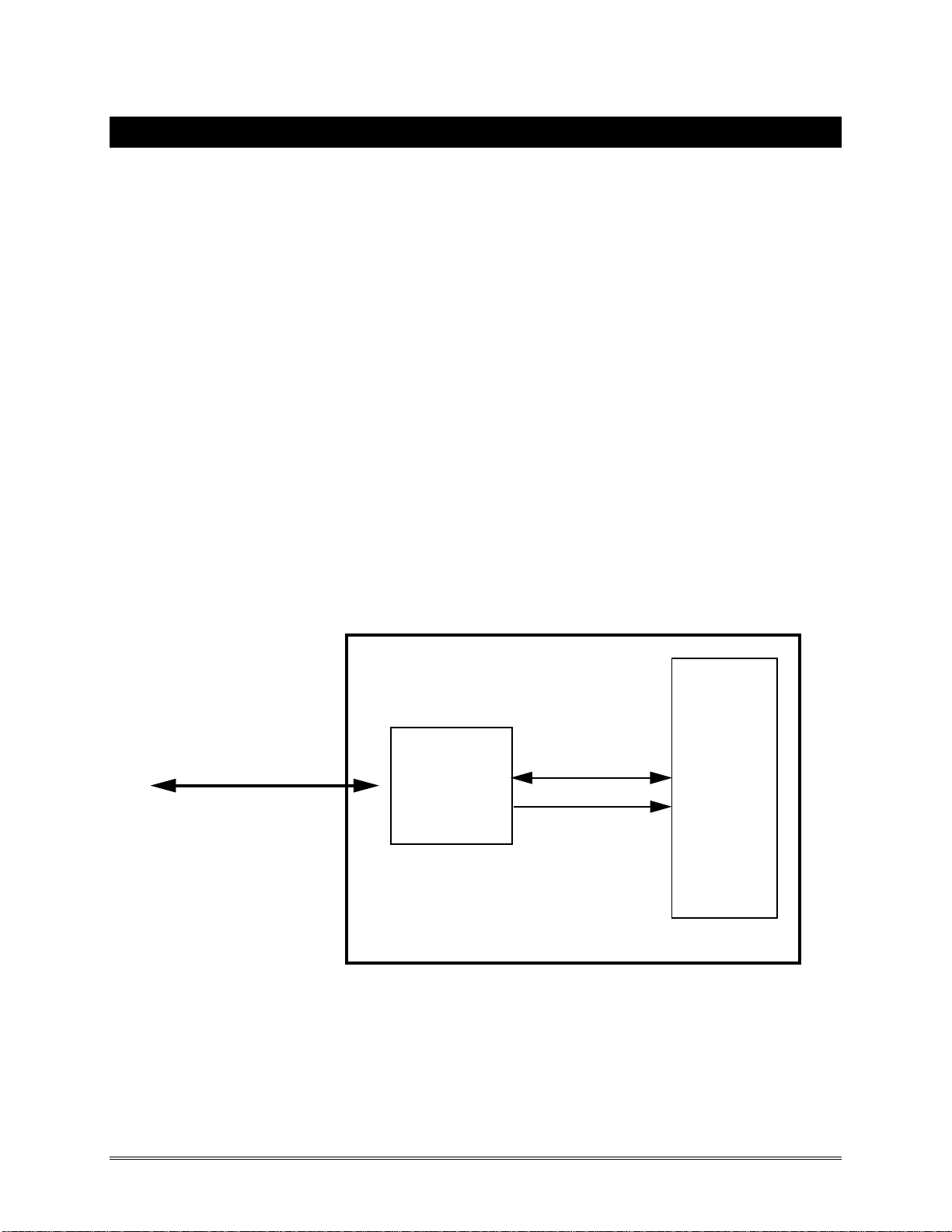
The MultiMediaCard provides up to 128 million bytes of memory using SanDisk Flash memory chips, which were
designed by SanDi sk especi ally for us e in mass s tora g e applic ation s. In addition t o the mass storage specific flash
memory chip, the MultiMediaCard includes an on-card intelligent controller which manages interface protocols and
data storage and retrieval, as well as Error Correction Code (ECC) algorithms, defect handling and diagnostics,
power management and clock control.
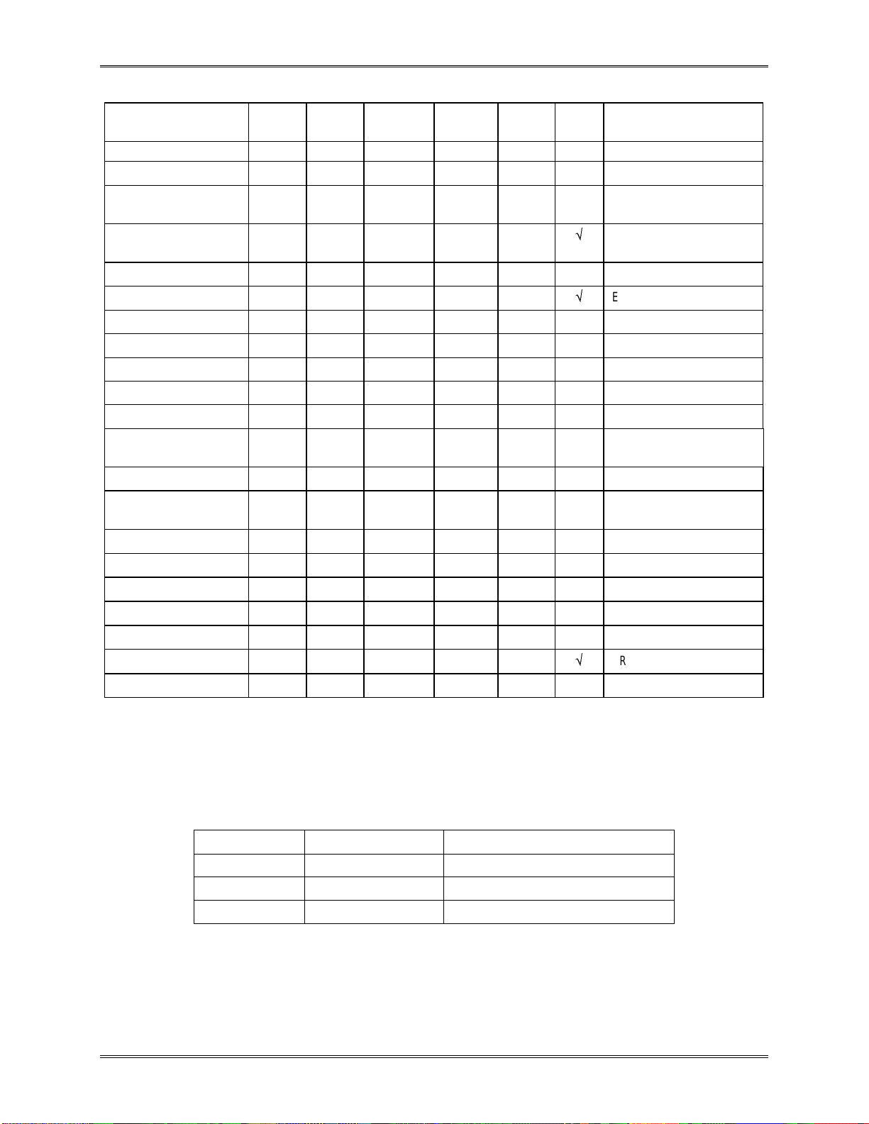
Data
In/Out
Control
Data
Flash
Modules
MultiMediaCard/SPI
SanDisk
Single
Chip
Controller
Interface
SanDisk MultiMediaCard
Figure 1-1. MultiMediaCard Block Diagram
MultiMediaCard Product Manual, Rev. 5.1 © 2002 SANDISK CORPORATION
1-1
Page 8

Introduction to the MultiMe d iaCard
1.1. Scope
This docu ment describ es the key featu re s and specificatio ns of the MultiMediaCard, as well as the information
required to int erface thi s product to a host system.
1.2. Pr oduct Models
The MultiMediaCard is available in the capacities shown in Table 1-1.
Table 1-1. MultiMediaCard Capacities
Model No. Capacities
SDMB-16 16 MB
SDMB-32 32 MB
SDMJ-64 64 MB
SDMJ-128 128 MB
SDMB = Binary NAND technology.
SDMJ = Multi Level Cell (MLC) NAND technology.
1.3. System Features
The MultiMediaCard Association Standard features are as follows:
•
Up to 128 Mbytes of data storage.
•
MultiMediaCard protocol compatible.
•
Supports SPI Mode.
•
Targeted for portable and stationary applications.
•
Voltage range:
−
Communication: 2.0-3.6V
−
Memory Access: 2.7-3.6V
•
Maximum data rate with up to 10 cards.
•
Correction of memory field errors.
•
Built-in write protection features (permanent and temporary).
•
Pre-erase mechani s m.
•
Variable clock rate 0-20 Mhz.
•
Multiple cards stackabl e on a single physical bus.
1-2 MultiMediaCard Product Manual, Rev. 5.1 © 2002 SANDISK CORPORATION
Page 9

Introduction to the MultiMe d iaCard
The perfor mance of the com municat ion channel is described in Table 1-2.
Table 1-2. MultiMediaCard/SPI Comparison
MultiMediaCard SPI
Three-wire serial data bus (Clock, command, data). Three-wire serial data bus (Clock, dataIn, dataOut) + card
specifi c CS signal.
Up to 64k cards addressable by the bus protocol. Card selection via a hardware CS signal.
Easy card identification. Not available.
Error -protected data transfe r. Optional. A non-protected data transfer mode is available.
Sequential and single/multiple block oriented data transfer . Single/Multiple block read/write*.
* Multiple sector Read/Write in SPI mode was approved by the MMCA and is included in MMCA system standard rev 3.1.
1.4. MultiM ediaCar d Standard
MultiMediaCards are fully compatible with the MultiMediaCard standard specification listed below:
The MultiMediaCard System Specification, Version 2.2
This specification may be obtained from:
MultiMediaCard Association
19672 Stevens Creek Blvd., Suite 404
Cupertino, CA 95014-2465
USA
Phone: 408-253-0441
Fax: 408-253-8811
Email: prophet2@mmca.org
http://www.mmca.org
1.5. Functional Description
SanDisk MultiMediaCards contain a high level, intelligent subsystem as shown in t he block diagram, Figure 1-1.
This intelligent (microprocessor) subsy stem prov id es many c ap abilities no t found in other types of memory cards .
These capabilities include:
•
Host independence from details of erasing and programming flash memory.
•
Sophisticated system for managing defects (analogous to systems found in magnetic di sk drives).
•
Sophi st i ca t ed system for err or recovery including a powerful error c orre ction code (ECC).
•
Power management for low power operation.
MultiMediaCard Product Manual, Rev. 5.1 © 2002 SANDISK CORPORATION 1-3
Page 10

Introduction to the MultiMe d iaCard
1.5.1. Flash Technology Independence
The 512 by te s ector size of the M u ltiM e diaCard is the same as that in an IDE magnetic dis k driv e. To write or read a
sector (or multiple sectors), the host computer software simply issues a Read or Write command to the
MultiMediaCard. This command contains the address. The host software then waits for the command to complete.
The host software does not get involve d i n the details of how the flash memory is erased, programmed or read. This
is extremely important as flash devices are expected to get more and more complex in the future. Because the
MultiMediaCard uses an intelligent on -board controller, the host system software will not require changing as new
flash memor y evolves. In other words, systems tha t support the Mu ltiMediaCard today will be able to access future
SanDisk MultiMediaCards built with new flash technology wit ho u t h av ing to update or change host software.
1.5.2. Defect and E rror Management
MultiMed iaC ards contain a sophisticated defect and error management system. T his system is analogous to the
systems found in magnetic disk drives and in many cases offers enhancement s. For instan ce, dis k drives do not
typically perform a read after write to confirm the data is written correctly because of the performance penalty that
would be incurred. MultiMediaCards do a read after write under margin conditions to verify that the data is written
correctly. In the rar e case that a bit is found to be de f ect ive, Mul ti M ediaCard s replace this bad bit with a spare bit
within the sector header. If necessary, MultiMediaCards will even replace the entire sector with a spare sector. This
is c omplete l y trans p a re nt to the ho st and does n ot co n s ume any user dat a sp ac e .
The MultiMediaCard’s soft error rate specification is much better than the magnetic disk drive specification. In the
ext remely rare c ase a read error do es occ ur , Mul tiMediaCard s have innovativ e algo rithms to rec ov e r the data. This is
similar to using retries on a disk drive but is much more sophisticated. The last line of defense is to employ a
powerful ECC to correct the data. If ECC is used to recover data, defective bits are replaced with spare bits to ensure
they do n ot cause any future problems.
These defect and error management systems coupled with the solid-state construction give MultiMediaCards
unparalleled reliability.
1.5.3. Endurance
SanDisk MultiMediaCards have a typical endurance specification for each sector of 100,000 writes (reading a
logical sector is unlimited). This far exceeds what is needed in nearly all applications of MultiMediaC ard s. F or
example, even very heavy use of the MultiMediaCard in cellular phones, personal communicators, pagers and voice
recorders will use only a fraction of the total endurance over the typical device’s lifetime. For instance, it would take
over 34 years to wear out an a rea on the MultiMediaCar d on which a file of any size (from 512 bytes to maximum
capacity) was rewritten 3 times per hour, 8 hours a day, 365 days per year.
With typical applications the endurance limit is not of any practical concern to the vast majority of users.
1-4 MultiMediaCard Product Manual, Rev. 5.1 © 2002 SANDISK CORPORATION
Page 11

Introduction to the MultiMe d iaCard
1.5.4. Automatic Sleep Mode
A unique feature of the SanDisk MultiMediaCard (and other SanDisk products) is automatic entrance and exit from
sleep mode. Upon completion of an operation, the MultiMediaCard will enter the sleep mode to conserve power if
no furth er comman ds are received withi n 5 msec. T he h ost does not have to tak e any action for this to occur. In most
systems, the MultiMediaCard is in sleep mode except when the host is accessing it, thus conserving power.
When the host is ready to acces s the MultiMediaCard and it is in sleep mode, any command issued to the
MultiMediaCard will cause it to exit sleep and respond.
1.5.5. Hot Insertion
Support for hot insertion will be required on the host, but will be supported through the connector. Connector
manufacturers will provide connectors that have power pins long enough to be powered before contact is made with
the other pins. Please see connector data sheets for m or e details. This approach is similar to that used in PCMCIA to
allow for hot insertion. This applies to both MultiMediaCard and SPI modes.
1.5.6. Mu ltiM ediaCard M ode
The following sections provide valuable information on the MultiMediaCard mode.
1.5.6.1. M ultiMediaCard S t andard Compliance
The MultiMediaCard is fully compliant with MultiMediaCard Standard Specification, version 2.2. Th e structure of
the Card Specific Data (CSD) register is compliant with CSD structure version 2.2.
1.5.6.2. Negotiating Operation Conditions
The MultiMediaCard supports the operation condition verification sequence defined in the MultiMediaCard
standard specifications. Should the MultiMediaCard host define an operating voltage range, which is not supported
by the MultiMediaCard it will put itself in an inactive state and ignore any bus communication. The only way to get
the card out of the inactive state is by powering it down and up again.
In addition, the host can explicitly send the card to the inactive state by using the GO_INACTIVE_STATE
command.
1.5.7. Card Acqu isition and Identi fication
The MultiMediaCard bus is a single master (MultiMediaCard host) and multi-slaves (cards) bus. The host can query
the bus and find out how many cards of which type are currently connected. The MultiMediaCard’s CID register is
pre-programmed with a unique card identification number that is used during the acquisition and identification
procedure.
MultiMediaCard Product Manual, Rev. 5.1 © 2002 SANDISK CORPORATION 1-5
Page 12

Introduction to the MultiMe d iaCard
In addition, the MultiMediaCard host can read the card’s CID register using the READ_CID MultiMediaCard
command. The CI D r egister is progra mmed durin g the MultiMediaCard testing and formatting procedure, o n the
manufacturing floor. The MultiMediaCard host can only read this register and not write to it.
1.5.7.1. Card St at us
MultiMed iaC ard statu s is stored in a 32-bit status register which is sent as the data field in the card response to host
commands. The Status register provides information about the card’s current state and completion codes for the last
host command.
The card status can be explicitly read (polled) with the SEND_STATUS command.
1.5.7.2. Memory Array Partitioning
Although the MultiMediaCard memory space is byte addressable with addresses ranging from 0 to the last byte, it is
not a simple byte array but divided into several structures.
Memory bytes are grouped into 512 byte blocks called sectors. Every block can be read, written and erased
individually.
Sectors are grouped into erase groups of 16 or 32 sectors depending on card size. Any combination of sectors within
one group, or any combination of erase group s can be er ased in a sing le erase command. A write comma nd
implicitly erases the memory before writing new data into it. An explicit erase command can be used for pre-erasing
memory, which will speed up the next write operation.
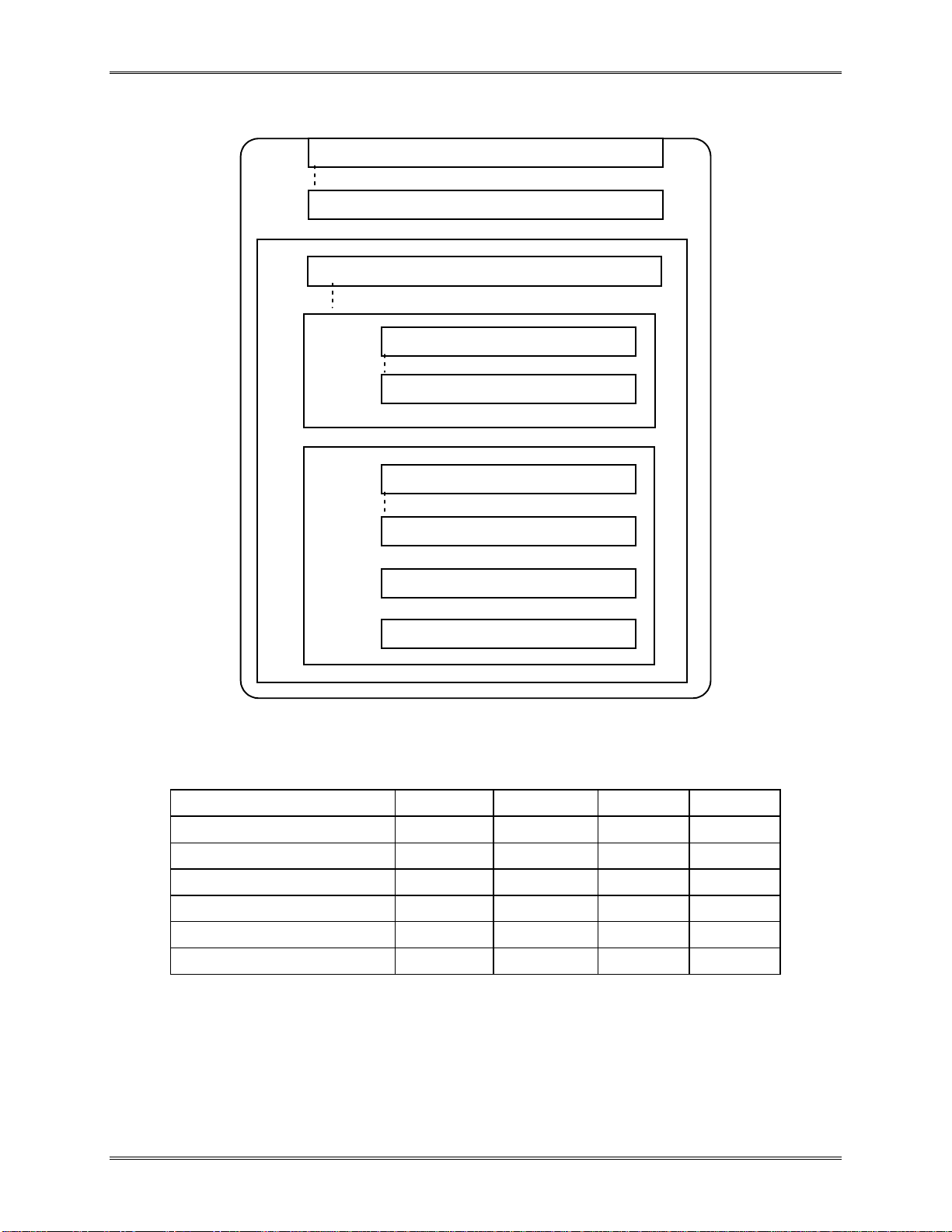
Erase groups are gr ou p ed into Wri te Prot ect Grou p s (WPG ) of 32 erase group s . Th e write/erase acces s to each WPG
can be limited individually. A diagram of the memory structure hierarchy is shown in Figure 1-2.
The number of various memory structures, for the different MultiMediaCards are summarized in Table 1-3. The last
(h ighest in address) WPG will be smaller and contain less than 32 erase groups.
1-6 MultiMediaCard Product Manual, Rev. 5.1 © 2002 SANDISK CORPORATION
Page 13
Introduction to the MultiMe d iaCard
WP Group N
WP Group 1
Erase Group m
Sec t or n
Erase Group 1
Write Protect Group 0
Erase Group 0
Sector 1: Bytes 512 - 1,023
Sec t or 0
Sec t or n
Sec t or 2
Sector 0: Bytes 0 - 511
Figure 1-2. Memory Array Partitioning
Table 1-3. Memory Array Structures Summary
Structure SDMB-16 SDMB-32 SDMJ-64 SDMJ-128
Bytes 16 MB 32 MB 64 MB 128 MB
Sector 31,360 62,720 125,440 250,880
Erase Group Size [sectors] 32 32 32 32
Number of Erase Groups 980 1,960 3,920 7,840
Write Protect Group Size [erase groups] 32 32 32 32
Number of Write Protec t Groups 31 62 123 245
NOTE: All measurements are in units per card.
MultiMediaCard Product Manual, Rev. 5.1 © 2002 SANDISK CORPORATION 1-7
Page 14
Introduction to the MultiMe d iaCard
1.5.7.3. Re ad and Write Operations
The MultiMediaCard supports two read/write modes as shown in Figure 1-3.
Single Block Mode Misalignment Error
Memory
Sectors
Memory
Sectors
Start
Address
(Read)
Memory
Sectors
Memory
Sectors
Start
Address
(Write)
Memory
Sectors
Memory
Sectors
Start
Address
(Read/Write)
Memory
Sectors
Multiple Block Mode
Memory
Sectors
Memory
Sectors
Address
Start
Memory
Sectors
Memory
Sectors
Memory
Sectors
Stop StopStart
Memory
Sectors
ReadWrite
Figure 1-3. Data Transfer Formats
Single Block Mode
In this mode, the host reads or writes one data block in a pre-specified length. The data block transmission is
protected with 16-bit CRC, which is generated by the sending unit a nd checked by the receiving unit.
Memory
Sectors
The block length for read operations is limited by the device sector size (512 bytes) , but can be as small as a single
byte. Misalignment is not allowed. Every data block must be contained in a single physical sector.
The block length for write operations must be identical to the sector size and the start address aligned to a sector
boundary.
Multiple Block Mode
This mode is similar to the single block mode, but the host can read/write multiple data blocks (all have the same
length), which will be stored or retrieved from contiguous memo ry add resses s tarting at the address specified in the
command.
The operation is terminated with a stop transmission c ommand. Misalignment and bloc k length restrictions apply to
multiple blocks as well, and are identical to the single bloc k read/write operations.
1-8 MultiMediaCard Product Manual, Rev. 5.1 © 2002 SANDISK CORPORATION
Page 15

Introduction to the MultiMe d iaCard
1.5.7.4. Data Protection i n the Flash Card
Every sector is protected with an Error Correction Code ( ECC). The ECC i s generated (in the memory card) wh en
the sectors are written and validated when the data is read. If defects are found, the data is corrected prior to
transmission to the host.
1.5.7.5. Erase
The sma llest era sable unit in the MultiMed iaCard is a sector. In order to speed up the erase procedure, multiple
sectors ca n be erased a t the same time. The era se o peration is divided into two stages:
Tagging—Selecting the Sectors for Erasing. To facilitate selection, a first command with the starting address is
followed by a second command with th e final address, and all sectors within this range will be selected for erase.
Erasing—Startin g th e Erase Process. The sectors are grouped into erase groups of 16 or 32 sectors. Tagging can
address se ctors or e ra se groups. Ei t her an arbitrary set of sectors withi n a single eras e gro u p , or an arbitrary selection
of erase groups may be erased at one time, but not both together. That is, the unit of measure for determining an
erase is either a sector or an erase group. If sectors are tagged, then all selected sectors must lie within the same
erase group. Tagging and erasing sectors must follow a strict command sequence.
1.5.7.6. Write Protecti on
Two card level write protection options are available: permanent and temporary. Both can be set using the
PROGRAM_CSD command (s ee sect ion 4.2.3). T he permanen t write pr ot ect bit, once set , cannot be cl eared . This
feature is implemented in the MultiMediaCard controller firmware and not with a physical OTP cell.
1.5.7.7. Cop y Bit
The content of a MultiMediaCard can be marked as an original or a copy using the copy bit in the CSD register.
Once t he Copy bit is set (marked as a copy) it cannot be cl eared. The Copy bit of the MultiMedia Car d is
programmed (during test and formatting on the manufacturing floor) as a copy. The MultiMediaCard can be
purchased with the copy bit set (copy) or cleared, indicating the card is a master. This feature is implemented in the
MultiMediaCard controller firmware and not with a physical OTP cell.
1.5.7.8. Th e CSD Reg ister
All the configuration information of the MultiMediaCard is stored in the CSD register. The MSB bytes of the
register contain manufacturer data. The two least significant bytes contain the host controlled data: the card Copy
and write protection, the user file format indication, and the user ECC register.
The host can read the CSD register and alter the host-controlled data bytes using the SEND_CSD and
PROGRAM_CSD commands (see section 4.2.3).
MultiMediaCard Product Manual, Rev. 5.1 © 2002 SANDISK CORPORATION 1-9
Page 16

Introduction to the MultiMe d iaCard
1.5.8. SPI Mode
The SPI mode is a secondary communication protocol for MultiMediaCards. This mode is a subset of the
MultiMediaCard protocol, designed to communicate with an SPI channel, common ly found in Motorola’s (and
lately a few other vendors’) microcontrollers.
1.5.8.1. Negotiating Operating Conditions
The operating condition negotiation function of the MultiMediaCard bus is not supported in SPI mode . The host
must work within th e valid voltage range (2.7 to 3.6) volts of the card.
1.5.8.2. Card Acq uisition and Ident ification
The card acquisition and identification function of the MultiMediaCard bus is not supported in SPI mode. The host
must k now th e num ber of car ds currently connected on the bus. Speci fi c card selection is done via the CS si g nal.
1.5.8.3. Card St at us
In SPI m ode only 16 bits (containing the err ors relevant to S P I mode) can be read out of t he MultiMediaCard status
register.
1.5.8.4. Memory Array Partitioning
Memory partitioning in SPI mode is equivalent to MultiMediaCard mode. All read and write commands are byte
addressable.
1-10 MultiMediaCard Product Manual, Rev. 5.1 © 2002 SANDISK CORPORATION
Page 17

Introduction to the MultiMe d iaCard
1.5.8.5. Re ad and Write Operations
The SPI mode, as defined in the MMCA Standard, version 2.2, supports only single block read/write. Additionally,
the SanDisk MultiMediaCard supports a multiple block read/write that was approved by the MMCA and will be
included in a future MultiMediaCard System Specification.
1.5.8.6. Data Transfer Rate
Same as for the MultiMediaCard mode when the card is operating in single block read/write mode.
1.5.8.7. Data Protection in the M ultiMediaCard
Same as for the MultiMediaCard mode.
1.5.8.8. Erase
Same as in MultiMediaCard mode.
1.5.8.9. Write Protectio n
Same as in MultiMediaCard mode.
MultiMediaCard Product Manual, Rev. 5.1 © 2002 SANDISK CORPORATION 1-11
Page 18

Introduction to the MultiMe d iaCard
This page intentionally lef t bl ank .
1-12 MultiMediaCard Product Manual, Rev. 5.1 © 2002 SANDISK CORPORATION
Page 19

2. Product Specifications
For all the followi n g sp ecifications, values are defined at ambient temperature and nominal supply voltage unless
otherwise st ated.
2.1. System Envir onm ental Specifications
Table 2-1. System Environment Specifications
Temperature Operating:
Non-Operating:
Humidity Operating:
Non-Operating:
ESD Protection Contact Pads:
Non Contact Pad Area:
Acoustic Noise: 0 dB
Vibration Operating:
Non-Operating:
Shock Operating:
Non-Operating:
Altitude (relative to sea level) Operating:
Non-Operating:
-25° C to 85° C
-40° C to 85° C
8% to 95%, non-condensing
8% to 95%, non-condensing
± 4kV, Human body model according to ANSI
EOS/ESD-S5.1-1998
± 8kV (coupling plane discharge)
± 15kV (air discharge)
Huma n body model per IEC61000-4-2
15 G peak to peak max.
15 G peak to peak max.
1,000 G max.
1,000 G max.
80,000 feet max.
80,000 feet max.
2.2. Typical System P ower R equir ements
Table 2-2. System Power Requirements
Operation @3.6V @2.7V
Read 25 20
Write 35 25
Sleep 50µA (typical)
150µA (m ax)
MultiMediaCard Product Manual, Rev. 5.1 © 2002 SANDISK CORPORATION
40µA (typical)
120µA (m ax)
2-1
Page 20

Product Specifications
2.3. System Perfor m ance
Table 2-3. System Performance
Typical Maximum
Block Read Ac cess Ti m e
Binary Produc ts
MLC Products
Block Write Access Time
Binary Produc ts
MLC Products
CMD1 to Ready (after power up) 50msec 500msec
Sleep to Ready 1msec 2msec
NOTES: All values quoted are under the following conditions:
1) Voltage range: 2.7 V to 3.6 V.
2) Temperature range: -25° C to 85° C.
3) Are independent of the MultiMediaCard clock frequency.
1.5msec
10msec
24msec
40msec
15msec
100msec
240msec
400msec
2.4. System Reliability and Maintenance
Table 2-4. System Reliability and Maintenance
MTBF > 1,000,000 hours
Preventive Maintenance None
Data Reliab ility < 1 non-recoverab le error in 1014 bits read
Endurance 100,000 write/erase cycles (typical)
2.5. Physical Specifications
Table 2-5 lists the physical specifications and Figure 2-1 shows MultiMediaCard physical dimensions.
Table 2-5. Physical Specifications
Weight 1.5 g. maximum
Length 32mm ± 0.1mm
Width 24mm ± 0.08mm
Thickness 1.4mm ± 0.1mm
2-2 MultiMediaCard Product Manual, Rev. 5.1 © 2002 SANDISK CORPORATION
Page 21
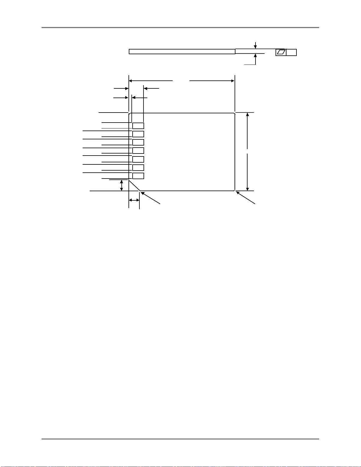
Product Specifications
0.2
1.4 ± 0.1
32.0 ± 0.1
4.5 min.
1.2 max.
0.00
3.10 max.
5.60 max.
8.10 max.
10.60 max.
13.10 max.
15.60 max.
18.10 max.
4.65 min.
7.15 min.
9.65 min.
12.15 min.
14.65 min.
17.15 min.
19.65 min.
24.00 ± 0.08
4.0 ± 0.1
4.0 ± 0.1
2 x R0.5 ± 0.1
All dimensions are in millimeters.
Figure 2-1. MultiMediaCard Dimensions
3 x R1.0 ± 0.1
MultiMediaCard Product Manual, Rev. 5.1 © 2002 SANDISK CORPORATION 2-3
Page 22

Product Specifications
This page intentionally l e f t bl ank .
2-4 MultiMediaCard Product Manual, Rev. 5.1 © 2002 SANDISK CORPORATION
Page 23
3. MultiM ediaC ard Interface Description
3.1. Physical Description
The MultiMediaCard has seven exposed cont acts on one s ide (see Figure 2-1). T he host is connected to the
MultiMediaCard using a seven- p i n connect or .
3.1.1. Pin Assignments in MultiMediaCard Mode
Table 3-1. MultiMediaCard Pad Definition
Pin # Name Type* MultiMediaCard Description
1 RSV NC Not Connected or Always ‘1’
2 CMD I/O/PP/OD Command/Response
3 VSS1 S Supply voltage ground
4 VDD S Supply voltage
5 CLK I Clock
6 VSS2 S Supply voltage ground
7 DAT[0] I/O/PP Data 0
* S=power supply; I=input; O=output; PP=push-pull; OD=open-drain; NC=not connected.
3.1.2. Pin Assignments in SPI Mode
Table 3-2 . SPI Pad Definition
Pin # Name Type* SPI Description
1 CS I Chip Select (Active low)
2 DataIn I Host to Card Commands and Data
3 VSS1 S Supply Voltage Ground
4 VDD S Supply Voltage
5 CLK I Clock
6 VSS2 S Supply Voltage Ground
7 DataOut O Card to Ho st Data and Status
* S=power supply; I=input; O=output.
MultiMediaCard Product Manual, Rev. 5.1 © 2002 SANDISK CORPORATION
3-1
Page 24
MultiMediaCard Interface Description
3.2. Multi M ediaC ar d Bus Topology
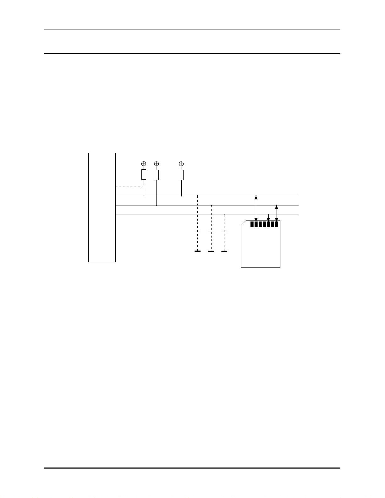
The MultiMediaCard bus has three communication lines and four supply lines (see Figure 3-1):
•
CMD—Command is a bi-directional signal. Host and card drivers are operating in two modes, open
drain and push pull.
•
DAT—Data is a bi-directional signal. Host and card drivers are operating in push pull mode.
•
CLK—Clock is a host to card signal. CLK operates in push pull mode.
•
VDD—VDD is the power supply line for all cards.
•
VSS[1:2]—VSS are two ground lines.
MultiMediaCard
Host
R
OD
= max (C , C , C )
C
BUS
R
1
DAT
2
R
CMD
C1C2C
3
CMD
DAT
CLK
3
1 2 3 4 5 6 7
MultiMediaCard
Figure 3-1. Bus Circuitry Diagram
The R
and R
is switched on and off by the host synchronously to the open-drain and push-pull mode transitions. R
OD
are pull-up resistors protec ting the CMD and the DAT line against bus f lo ating w hen no card is inse rted o r
CMD
when all card drivers are in a hi-impedance mode.
A consta nt cu rr ent sou rce can repla ce the R
rising and falling edges). If the host does not allow the switchable R
in order to achieve better performance (constant slopes for the signal
OD
implementation, a fix R
OD
can be used.
CMD
Consequently the maximum operating frequency in the open drain mode has to be reduced in this case.
DAT
Hot Insertion/Removal
Hot insertion a nd removal are allowed. The SanDisk MultiMediaCard will not be damaged b y inserting or removing
it into the MultiMediaCard bus even when the power is up:
•
The inserted card will be properly reset also when CLK carries a clock frequency fPP.
•
Data transfer failures induced by removal/insertion should be detected by the bus master using the
CRC codes that suffix every bus transaction.
3-2 MultiMediaCard Product Manual, Rev. 5.1 © 2002 SANDISK CORPORATION
Page 25

MultiMediaCard Interface Description
3.2.1. Power Pro tection
Cards can be inserted/removed into/from the bus without damage. If one of the supply pins (V
DD or VSS)
is not
connected properly, then the current is drawn through a data line to supply t he c ar d .
If th e hot in sertion feature is implemented in the host, then the host has to withstand a shortcut between V
DD
and V
SS
without damage.
3.3. SP I Bus Topology
The MultiMediaCard SPI interface is compatible with SPI hosts available on the market. As with any other SPI
device, the MultiMediaCard SPI channel consists of the following four signals:
•
CS—Host to card Chip Select signal.
•
CLK—Host to card clock signal.
•
DataIn—Host to card data signal.
•
DataOut—Card to host data signal.
Another SPI co mmo n characteristic, which is implemente d in the MultiMediaCard as well, is byte transfers. All d ata
tokens are multiples of 8-bit bytes and are always byte-aligned to the CS signal. The SPI standard defines the
physical link only and not the complete data transfer protocol. The MultiMediaCard uses a subset of the
MultiMediaCard protocol and com ma nd set.
The MultiMediaCard identification and addressing algorithms are replaced by a hardware Chip Select (CS) signal.
There are no broadca s t comma nds. A car d ( slave) is selected for every co mmand, by a sserting (active low) the CS
signal (see Figure 3-2).
The CS signal must be continuously active for the duration of the SPI transaction (command, response and data).
The only exc epti on is card pro gr amming time. At this time, the host can de-assert the CS signal without affecting the
programming process.
The bi-directional CMD and DAT lines are replaced by unidirectional dataIn and dataOut signals. This prevents
command execution while data is being read or written and, therefore, eliminates sequential and multi block
read/ write ope ra tions. On ly single block read/ wri te is suppor t ed by the S PI channel.
MultiMediaCard Product Manual, Rev. 5.1 © 2002 SANDISK CORPORATION 3-3
Page 26
MultiMediaCard Interface Description
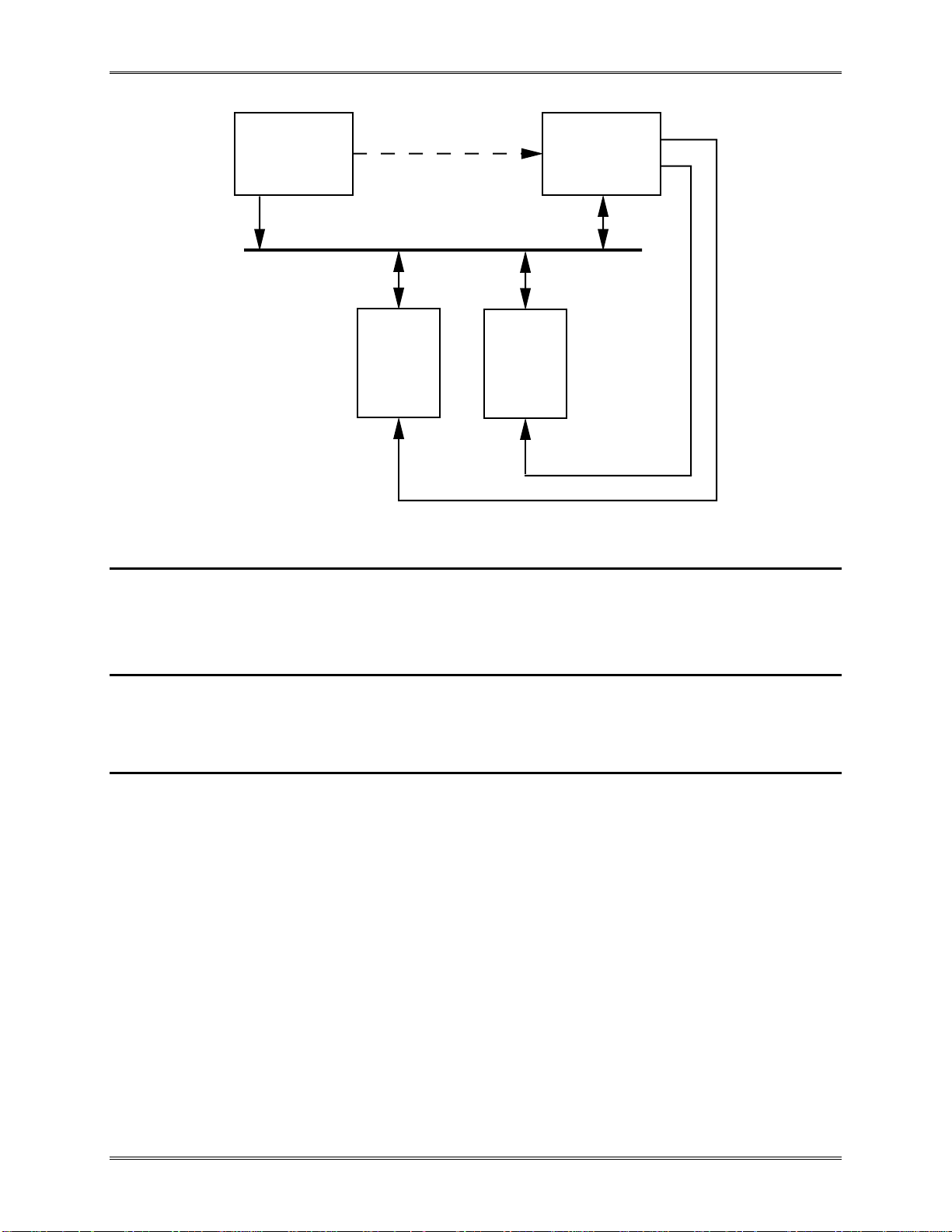
Power
Supply
3.3.1. Power Pro tection
SPI Bus (CLK, DataIN, DataOut)
SPI
Card
SPI
Card
Figure 3-2. MultiMediaCard Bus System
SPI Bus
Master
CS
CS
Same as for MultiMediaCard mode.
3.4. Electrical Interface
The following sections provide valuable information on the electrical interface.
3.4.1. Power- up
The power up of the MultiMediaCard bus is handled locally in each MultiMediaCard and in the bus master.
Figure 3-3 shows a power-up diagram.
3-4 MultiMediaCard Product Manual, Rev. 5.1 © 2002 SANDISK CORPORATION
Page 27
MultiMediaCard Interface Description
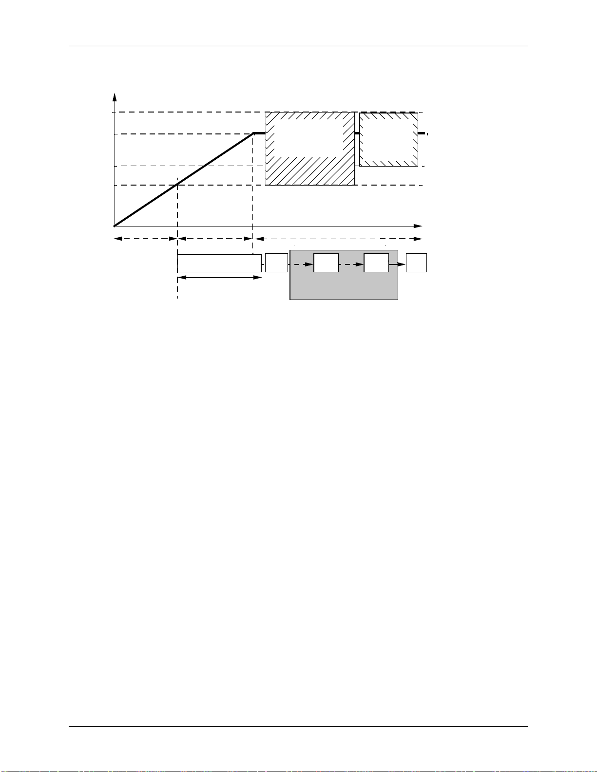
Logic working level
Supply voltage
Supply ramp u p time
Bus master sup ply voltage
CMD1
VDD max
Power up time
Initialization delay:
The maximum of
CMD2
N
CC
N
CC
N
CC
1 msec, 7 4 clock cycles
and suppl y ramp up time
Initialization sequenc e
CMD1
CMD1
VDD min
time
First CMD1 to card is ready.
Card logic working
voltage range
Optional repetitions of CMD1
until no cards are responding
with busy bit set.
Memory field
working
voltage
range.
Figure 3-3. Power-up Diagram
After power-up, including hot insertion (inserting a card when the bus is operating), the MultiMediaCard enters the
Idle State. During this state, the MultiMediaCard ignores all bus transactions until CMD1 is received.
CMD1 is a special synchronization command used to negotiate the operation voltage range and to poll the cards
until they are out of their power-up sequence. Besides the operation voltage profile of the cards, the response to
CMD1 contains a busy fl ag, indicating that the card is still w ork ing on it s pow er -up p ro cedu re and is not ready for
identific atio n. This bit informs the host that at least one card is not ready. The host has to wait (and continue to poll
the cards) until this bit is cleared. The MultiMediaCard shall complete its initialization procedure within 500msec.
Getting individual cards, as well as the whole MultiMediaCard system, out of Idle State is up to the responsibility of
the bus master. Since the power-up time and the supply ramp up time depend on application parameters such as the
maximum number of MultiMediaCards, the bus length and the power supply unit, the host must ensure that the
power is built up to the operating level (the same level which will be specified in CMD1) before CMD1 is
transmitted.
After power-up, the host starts the clock and sends the initializing sequence on the CMD line. This sequence is a
contiguous stream of logical ones. The sequence length is the maximum of 1msec, 74 clocks or the supply ramp up
time. The additional ten clocks (beyond the 64 clocks after which the card should be r eady for communication) are
provided to eliminate power-up synchronization problems.
MultiMediaCard Product Manual, Rev. 5.1 © 2002 SANDISK CORPORATION 3-5
Page 28
MultiMediaCard Interface Description
3.4.2. Bus Operating Conditions
SPI Mode bus operating conditions are identical t o MultiMediaCard Mode bu s op erating condition s. The CS (chip
select) signal timing is identical to the input signal timing (see Figure 3-5).
Table 3-3 . Bus Operating Conditions
General
Parameter Symbol Min. Max. Unit Remark
Peak voltage on all lines -0.5 3.6 V
All Inputs
Input Leakage Current -10 10
All Outputs
Output Leakage Current -10 10
µA
µA
Power supply voltage
Parameter Symbol Min. Max. Unit Remark
Supply voltage VDD 2.0 3.6 V
Supply vol tage differenti als (V
The current consumption of any card during the power-up procedure must not exceed 10 mA.
, V
) -0.5 0.5 V
SS1
SS2
Capacitance
Parameter Symbol Min. Max. Unit Remark
V
capacitance C (V
DD
3.0
DD)
µF
Bus Signal Line Load
The total capacitance CL of each line of the MultiMediaCard bus is the sum of the bus master capacitance CHOST,
the bu s ca p acitance C BUS its elf, and t he cap acitance C C ARD of each card connected t o t his line:
CL = CHOST + CBUS + N
CCARD
Where N is th e num ber of connected ca rds. Given the requi rement that th e sum of the host and bus ca p acitances not
exceed 30 pF for up to 10 cards, and 40 pF for up to 30 cards, the values in Table 3-4 must not be exceeded.
Table 3-4 . Host and Bus Capacitie s
Parameter Symbol Min. Max. Unit Remark
Pull-up resistance RCMD
RDAT
Bus signal line capacitance CL 250 pF
Bus signal line capacitance CL 100 pF
Single card capacitance CCARD 7 pF
Maximum signal line inductance 16 nH
50 100
kΩ
To prevent bus floating
fPP # 5 MHz, 30 cards
fPP # 20 MHz, 10 cards
fPP # 20 MHz
3-6 MultiMediaCard Product Manual, Rev. 5.1 © 2002 SANDISK CORPORATION
Page 29
MultiMediaCard Interface Description
A
A
3.4.3. Bus Signal Levels
Since the bus can be supplied with a variable supply voltage, all signa l levels are related to the supply voltage (see
Figure 3-4).
V
V
DD
Input
High
Level
Input
Low
Level
V
V
OH
IH
Undefined
V
IL
V
OL
AAAAAAA
AAAAAAA
V
SS
t
Output
High
Level
Output
Low
Level
Figure 3-4. Bus Signal Levels
3.4.4. Open - D rain Mo de Bus Signal Level
Table 3-5. Open Drain Mode Bus Signal Level
Parameter Symbol Min. Max. Unit Conditions
Output HIGH voltage VOH
Output LOW voltage VOL 0.3 V IOL = 2 mA
V
-0.2
DD
V
IOH = -100 µA
The inp ut levels are identic al with the push-pull mode bus signal levels.
3.4.5. Push-pull Mode Bus Sign al Level
To meet the requ ireme nts of the JEDEC specification JESD8-1A, the card input and output voltages shall be within
the specified r a nges in T a ble 3- 6 for a ny VDD of the allowed voltage ran ge.
Table 3-6. Push-Pull Mode Bus Signal Level
Parameter Symbol Min. Max. Unit Conditions
Output HIGH voltage VOH
Output LOW voltage VOL
Input HIGH voltage VIH
Input LOW voltage VIL VSS-0.3
0.75∗VDD
0.625∗VDD
V
0.125∗VDD
VDD + 0.3 V
0.25∗VDD
IOH=-100 µA
(min.)
@V
DD
V
IOL=100 µA
@V
(min.)
DD
V
MultiMediaCard Product Manual, Rev. 5.1 © 2002 SANDISK CORPORATION 3-7
Page 30
MultiMediaCard Interface Description
3.4.6. Bus Timing
SanDisk’s MultiMediaCa rds clock data in on the rising edge and out on the falling edge.
T
PP
t
THL
t
WL
t
TLH
t
ISU
Clock
Input
Output
t
WH
t
IH
V
IH
V
IL
V
IH
V
IL
V
OH
NOTE: Data in the shaded areas is not valid.
Figure 3-5. Timing Diagram Data Input/Output Referenced to Clock
Parameter Symbol Min. Max. Unit Remark
Clock CLK (All values are referred to min. (VIH) and max. (VIL)
Clock Frequenc y Data Transfer Mode (PP) fPP 0 20 MHz
Clock Frequenc y Identif i cation Mode (OD) fOD 0 400 kHz
Clock Low Time tWL 10 ns
Clock High Time tWH 10 ns
Clock Rise Time t
Clock Fall Time t
Clock Low Time tWL 50 ns
Clock High Time tWH 50 ns
Clock Rise Time t
Clock Fall Time t
t
OH
Table 3-7. Bus Timing
10 ns
TLH
10 ns
THL
50 ns
TLH
50 ns
THL
t
OSU
V
OL
C
L
(10 cards)
C
L
(30 cards)
C
L
(10 cards)
C
L
(10 cards)
C
L
(10 cards)
C
L
(10 cards)
C
L
(30 cards)
C
L
(30 cards)
C
L
(30 cards)
C
L
(30 cards)
• 100 pF
• 250 pF
• 100 pF
• 100 pF
• 100 pF
• 100 pF
• 250 pF
• 250 pF
• 250 pF
• 250 pF
3-8 MultiMediaCard Product Manual, Rev. 5.1 © 2002 SANDISK CORPORATION
Page 31
MultiMediaCard Interface Description
Parameter Symbol Min. Max. Unit Remark
Inputs CMD, DAT (referenced to CLK)
Input set-up ti me t
Input hold time tIH 3 ns
Outputs CMD, DAT (referenced to CLK)
Output set-up ti m e t
Output hold time tOH 5 ns
3 ns
ISU
5 ns
OSU
3.5. MultiM ediaCar d Registers
There is a set of six r egisters w ith in the ca rd interface. The OCR, CID and CSD r egisters carry the card
configuration information. The RCA register holds the card-relative communication address for the current session.
3.5.1. Operating Conditions Register (OCR)
The 3 2-bit O C R register stores the VDD voltage profile of the card. The MultiMediaCard is capable of executing the
voltage recognition procedure (CMD1) with any standard MultiMediaCard host using operating voltages from 2 to
3.6 Volts.
Accessing the data in the memory array, however, requires 2.7 to 3.6 Volts. The OCR shows the voltage range in
which the card data can be accessed. Table 3-8 list s the OCR Regi s ter definitions and Table 3-9 describes t h e
str u ctur e of the OCR r egister.
Table 3-8 . OCR Regi ster Defi ni t i on
OCR Bit VDD Voltage Window
0-7 Reserved
8 2.0-2.1
9 2.1-2.2
10 2.2-2.3
11 2.3-2.4
12 2.4-2.5
13 2.5-2.6
14 2.6-2.7
15 2.7-2.8
16 2.8-2.9
17 2.9-3.0
18 3.0-3.1
19 3.1-3.2
20 3.2-3.3
21 3.3-3.4
22 3.4-3.5
23 3.5-3.6
24-30 Reserved
31 Card power up status bit (busy)
MultiMediaCard Product Manual, Rev. 5.1 © 2002 SANDISK CORPORATION 3-9
Page 32

MultiMediaCard Interface Description
The level coding of the OCR register is as follows:
•
Restricted voltage windows=LOW
•
Card busy=LOW (bit 31)
The least significant 31 bits are constant and will be set as described in Figure 3-6. If bit 32 (the busy bit) is set, it
informs the host that the card power up procedure is finished.
00h
24
FFh
16
80h
8
00h
0
Reserved
Operating
Voltage Range
2.7 – 3.6 volt
Reserved
Busy Bit
Figure 3-6. OCR Structure
3.5.2. Card Ident ification (CID) Register
The CID register is 16 bytes long and contains a unique card identification number as listed in Table 3-9. It is
programmed during card manufacturing and cannot be changed by MultiMediaCard hosts.
Table 3-9. CID Fields
Name Type Width CID—Slice CID—Value Comments
Manufacturer ID (MID) Binary 8 [127:120] 0x02 The manufacturer IDs are controlled and
assigned by the MultiMediaCard
Association.
OEM/Application ID (OID) Binary 16 [119:104] 0x0000 Identifies the card OEM and/or the card
contents. The OID is assigned by the
MMCA. This field may be spec i fically
configured for OEM customers.
Product Name (PNM) String 48 [103:56] See Note 1 6 ASCII characters long
Product Revision (PRV) BCD 8 [55:48] See Note 2 Two binary coded decimal digits
Serial Number (PSN) Binary 32 [47:16] 32 Bits unsigned integer
Manufacturi ng Date Code
(MDT)
CRC7 checksum (CRC) Binary 7 [7:1] See Note 4 Calculated
Not used, always ‘1’ 1 [0:0]
NOTE 1: Model Name
Name in CD Field
SDMB-16 SDM016
SDMB-32 SDM032
SDMJ-64 SDM064
SDMJ-128 SDM128
BCD 8 [15:8] See Note 3 Manufacturing date—mm/yy
(offset from 1997)
3-10 MultiMediaCard Product Manual, Rev. 5.1 © 2002 SANDISK CORPORATION
Page 33

MultiMediaCard Interface Description
NOTE 2: The product revision is composed of two Binary Coded Decimal (BCD) digits, four bits each, representing an “n.m”
revision number. The “n” is the most significant nibble and the “m” is the least significant nibble. Example: The PRV
binary value filed for product revision “6.2” will be: 0110 0010.
NOTE 3: As an examp le, this field value for a March 2001 manufacturing date will be: 0011 0100.
NOTE 4: The CRC Checksum is computed by the following formula:
CRC Calculation: G(x)=x7+3+1
M(x)=(MID-MSB)*x119+...+(CIN-LSB)*x0
CRC[6...0]=Remainder[(M(x)*x7)/G(x)]
3.5.3. Card Specific Data (CSD) Register
The CSD register contains all the configuration information required in order to access the card data.
In the table below, the Cell Type column defines the CSD field as Read only (R), One Time Programmable (R/W)
or erasable (R/W/E). This table shows, for each field, the value in “real world” units and coded according to the
CSD structu re. The Model Dependent colu mn mar ks (with a check ma rk — √) the CSD fields that are model
dependent.
Table 3-10. CSD Register
Field
CSD_STRUCTURE 2 R [127:126] V1.2 1 CSD Structure
SPEC_VERS 4 R [125:122] V2.2 2 MultiMediaCard Specification
- 2 R [121:120] 0 0 Reserved
TAAC
Binary
MLC
NSAC 8 R [111:104] 0 0 Data Read Access-Time-2 in
TRAN_SPEED 8 R [103:96] 20MHz 0x2A Max. Data Transfer Rate
CCC 12 R [95:84] See note1 0x0F5 Card Command Classes
READ_BL_LEN 4 R [83:80] 512 9 Max. Read Data Block Length
READ_BL_PARTIAL 1 R [79:79] Yes 1 Partial Blocks for Read
WRITE_BLK_MISALIGN 1 R [78:78] No 0 Write Block Misalignment
READ_BLK_MISALIGN 1 R [77:77] No 0 Read Block Misalignment
DSR_IMP 1 R [76:76] No 0 DSR Implemented
- 2 R [75:74] 0 0 Reserved
Width
[bits]
8
8
Cell
Type
CSD-slice
R
R
[119:112]
[119:112]
CSD
Value
1.5msec
10msec
CSD
Code
0x0F
0x0F
Model
Dep.
Description
Version
Data Read Access-Time-1
Data Read Access-Time-1
CLK Cycles (NSAC*100)
Allowed
C_SIZE 12 R [73:62]
VDD_R_CURR_MIN 3 R [61:59] 60mA 6 Max. Read Current @VDD Min.
VDD_R_CURR_MAX 3 R [ 58:56] 80mA 6 Max. Read Current @VDD
√
De vi ce Size (C _SIZE)
1) This SanDisk product does not support the following classes: I/O, application specific, stream writ e, and str eam
read.
MultiMediaCard Product Manual, Rev. 5.1 © 2002 SANDISK CORPORATION 3-11
Page 34
MultiMediaCard Interface Description
Field
VDD_W_CURR_MIN 3 R [55:53] 60mA 6 Max. Write Current @ VDD Min.
VDD_W_CURR_MAX 3 R [52: 50] 80mA 6 Max. Write Current @VDD
C_SIZE_MULT 3 R [49:47]
SECTOR_SIZE 5 R [46:42] 1 0 Erase Sector Size
ERASE_GRP_SIZE 5 R [41:37] √ Erase Group Size
WP_GRP_SIZE 5 R [36:32] 32 0x1F Write Protect Group Size
WP_GRP_ENABLE 1 R [31:31] Yes 1 Write Protect Group Enable
DEFAULT_ECC 2 R [30:29] None 0 Manufacturer Default ECC
R2W_FACTOR 3 R [28:26] 1:4 2 Read to Write Speed Factor
WRITE_BL_LEN 4 R [25:22] 512 9 Max. Write Data Block Length
WRITE_BL_PARTIAL 1 R [21:21] No 0 Partial Blocks for Write
- 5 R [20:16] 0 0 Reserved
FILE_FORMAT_GRP 1 R/W [15:15] 0 0 Indicates File Format of
Width
[bits]
Cell
Type
CSD-slice
CSD
Value
CSD
Code
Model
Dep.
√
Device Size Multiplier
Description
Max.
Max.
(C_SIZE_MULT)
Allowed
Selected Group
COPY 1 R/W [14:14] Copy 1 Copy Flag (OTP)
PERM_WRITE_PROTECT 1 R/W [13:13] No 0 Permanent Write Protection
TMP_WRITE_PROTECT 1 R/W/E [12:12] No 0 Temporary Write Protection
FILE_FORMA T 2 R/W [11:10] 0 0 File Format of Card
ECC 2 R/W/E [9:8] None 0 ECC Code
CRC 7 R/W/E [7:1]
- 1 - [0:0] 1 1 Not Used, Always ‘1 ’
√
CRC
The following sections describe the CSD fields and the relevant data types. If not explicitly defined otherwise, all bit
strings are interpreted a s binary code d numbers starting with the left bit first.
CSD_STRUCTURE—Describes the version of t he CSD st ructure.
Table 3-11. CSD Register Structure
CSD_STRUCTURE CSD Structure Version Valid for MultiMediaCard Protocol Version
0 CSD version No. 1.0 MultiMediaCard protocol version 1.0-1.2
1 CSD version No. 1.1 MultiMediaCard protocol version 1.4-2.2
2—3 Reserved Reserved
MMC_PROT—Defines the MultiMe d iaC ard protocol version supported by the c ar d. I t i n cludes the definition of
the command set and the card responses. The card identification procedure is compatible for all protocol versions.
3-12 MultiMediaCard Product Manual, Rev. 5.1 © 2002 SANDISK CORPORATION
Page 35

MultiMediaCard Interface Description
Table 3-12. MultiMediaCard Protocol Version
SPEC_VERS MultiMediaCard Protocol Version
0 M ultiMediaCard prot ocol version 1.0-1.2
1 M ultiMediaCard prot ocol version 1.4
2 M ultiMediaCard prot ocol version 2.0-2.2
3-15 Reserved
TAAC—Defines the asynchronous part (relative to the MultiMediaCard clock (CLK)) of the read access time.
Table 3-1 3 . TAAC Access Time D efinition
TAAC Bit
Position
2:0 time exponent
0=1ns, 1=10ns, 2=100ns, 3=1µms, 4=10µms, 5=100µm s,
6=1ms, 7=10ms
6:3 time mantissa
0=Reserved, 1=1.0, 2=1.2, 3=1.3, 4=1.5, 5=2.0, 6=2. 5, 7=3.0,
8=3.5, 9=4.0, A=4.5, B=5. 0, C=5.5, D=6.0, E=7.0, F=8. 0
7 Reserved
Code
NSAC—Defines the wors t case for t he clock dependent fac tor of the data access time. The unit for NSAC is 100
clock cycles. T herefore, t he ma ximal val ue for t he clock depende nt part of t he read access time is 25.5k clock
cycles.
The total read access time N
as expressed in the Table 5-12 is the sum of TAAC and NSAC. It has to be computed
AC
by the host for the actual c lock rate. The read access time s hould be inte rpreted as a typic al de lay f or the first data bit
of a data block or stream from the end bit on the read commands.
TRAN_SPEED—Table 3-14 defines the maximum data transfer rate TRAN_SPEED.
Table 3-14. Maximum Data Transfer Rate Definition
TRAN_SPEED Bit Code
2:0 transfer rate exponent
0=100kbit/s, 1=1Mbit/ s, 2=10Mbit/s, 3=100Mbit /s, 4...
7=Reserved
6:3 time mantissa
0=Reserved, 1=1.0, 2=1.2, 3=1.3, 4=1.5, 5=2.0, 6=2. 5, 7=3.0,
8=3.5, 9=4.0, A=4.5, B=5. 0, C=5.5, D=6.0, E=7.0, F=8. 0
7 Reserved
CCC—The MultiMediaCard command set is divided into subsets (command classes). The card command class
register CCC defines which command classes are supported by this card. A value of ‘1’ in a CCC bit means that the
corresponding command class is supported. For command class definition refer to Table 5-5.
MultiMediaCard Product Manual, Rev. 5.1 © 2002 SANDISK CORPORATION 3-13
Page 36

MultiMediaCard Interface Description
CCC Bit Supported Card Command Class
Table 3-1 5 . Supporte d Card Command Classes
0 class 0
1 class 1
......
11 class 11
READ_BL_LEN—The data block length is computed as 2
READ_BL_LEN
. The block length m igh t therefo re be in the
range 1, 2, 4. . . 2048 bytes.
Table 3-16. Data Block Length
READ_BL_LEN Block Length
0 20 = 1 Byte
1 21 = 2 Bytes
......
11 211 = 2048 Bytes
12-15 Reserved
READ_BL_PARTIAL—Defines whether partial block sizes can be used in block read commands.
READ_BL_PARTIAL=0 means that only the READ_BL_LEN block size ca n be used for block-oriented data
transfers.
READ_BL_PARTIAL=1 means that smaller blocks can be used as well. The minimum block size will be equal to
minimum addressable unit (one byte)
WRITE_BLK_MISALIGN—Defines if the data block to be written by one command can be spread over more
than one physical block of the memory device. The size of the memory block is defined in WRITE_BL_LEN.
WRITE_BLK_MISALIGN=0 signals that crossing physical block boundaries is invalid.
WRITE_ BLK_ MISALI GN=1 signals that crossing physical blo ck bo u ndaries is allowed.
READ_BLK_MISALIGN—Defines if the data block to be read by one command can be spread over more than
one physical block of the memory device. The size of the memory block is defined in READ_BL_LEN.
READ_BLK_MISALIGN=0 signals that crossing physical block boundaries is invalid.
READ_BLK_MISALIGN=1 signals that crossing physical block boundaries is allowed.
DSR_IMP—Defines if the configur able driver s tage i s integ rated on the ca rd. If set, a dr iver stage regis ter ( D SR)
must be implemented also.
3-14 MultiMediaCard Product Manual, Rev. 5.1 © 2002 SANDISK CORPORATION
Page 37

MultiMediaCard Interface Description
Table 3-1 7 . DSR Implementation Code Table
DSR_IMP DSR Type
0 no DSR implemented
1 DSR implemented
C_SIZE (Device Size)—This pa ram eter is used to comp u te the car d ca pacity. The m emory capacity of th e card i s
computed from the entries C_SIZE, C_SIZE_MULT and READ_BL_LEN as follows:
memory capacity = BLOCKNR * BLOCK_LEN
Where:
BLOCKNR = (C_SIZE+1) * MULT
MULT = 2
BLOCK_LEN = 2
C_SIZE_MULT+2
READ_BL_LEN
(C_SIZE_MULT < 8)
(READ_BL_LEN < 12)
Therefore, the maximum capacity that can be coded is 4096*512*2048 = 4 GBytes. Example: A four MByte card
with BLOCK_LEN = 512 can be coded with C_SIZE_MULT = 0 and C_SIZE = 2047.
VDD_R_CURR_MIN, VDD_W_CURR_MIN—The minimum values for read and write currents on VDD power
supply are coded as in Table 3-18.
Table 3-18. V
VDD_R_CURR_MIN
VDD_W_CURR_MIN
2:0 0=0.5mA; 1=1mA; 2=5mA; 3=10mA; 4=25mA; 5=35mA;
Minimum Current Consumption
DD
Code For Current Consumption @ V
6=60mA; 7=100mA
DD
VDD_R_CURR_MAX, VDD_W_CURR_MAX—The maximum values for read and write currents on VDD
power supply are coded as in Table 3-19.
Table 3-19. V
VDD_R_CURR_MAX
VDD_W_CURR_MAX
2:0 0=1mA; 1=5mA; 2=10mA; 3=25m A ; 4=35mA; 5=45mA;
Maximum Current Consumption
DD
Code For Current Consumption @ V
6=80mA; 7=200mA
DD
C_SIZE_MULT (Device Size Multiplier)—This parameter is used for coding a factor MULT for computing the
total device size (see ‘ C _SIZE’ ). The fact or MULT i s defi ned as 2
Table 3-20. Multiply Factor For The Device Size
C_SIZE_MULT MULT
0 22 = 4
1 23 = 8
2 24 = 16
3 25 = 32
4 26 = 64
5 27 = 128
6 28 = 256
7 29 = 512
MultiMediaCard Product Manual, Rev. 5.1 © 2002 SANDISK CORPORATION 3-15
C_SIZE_MULT+2
.
Page 38

MultiMediaCard Interface Description
SECTOR_SIZE—The si ze of an erasable sector. T he content of this r eg ister is a 5- bi t bin ary coded value, defining
the num ber of writ e blocks (see WRITE_BL_LEN). The actual s ize is comp uted by increasing t his n umber by one.
A value of zero m e an s 1 write block, 31 mean s 3 2 blocks.
ERASE_GRP_SIZE—The size of an erasable group. The contents of this register is a 5-bit binary coded value,
defin ing t he n u mber of sect ors (see SEC TOR_SIZE ). The act ual size is comp u ted by increasin g this number by one.
A value of zero means 1 sector, 31 means 32 sectors.
WP_GRP_SIZE—The size of a write protected group. The contents of this register is a 5-bit binary coded value,
defin ing t he number of Erase Grou p s (see ERASE_G RP_ S I ZE). The a ctual size is comput ed by increasing this
number by one. A value of zero means 1 erase group, 31 means 32 erase groups.
WP_GRP_ENABLE—A value of ‘0’ means no group write protection possible.
DEFAULT_ECC—Set by the card manufactur er. I t defines the ECC code that i s recommended for use. T he field
definition is the same as for the ECC field described later.
R2W_FACTOR—Defines the typical block program time as a multiple of the read access time. Table 3-21 defines
the fi eld form at.
Table 3-21. R2W_FACTOR
R2W_FACTOR Multiples of Read Access Time
0 1
1 2 (write half as fast as read)
2 4
3 8
4 16
5 32
6, 7 Reserved
WRITE_BL_LEN—Block length for write operations. See READ_BL_LEN for field coding.
WRITE_BL_PARTIAL—Defines whether partial block sizes can be used in block write commands.
WRITE_BL_PARTIAL=‘0’ means that only the WRITE_BL_LEN block size can be used for block oriented data
write.
WRITE_BL_PARTIAL=‘1’ means that smaller blocks can be used as well. The minimum block size is one byte.
FILE_FORMAT_GROUP—Indicates the selected group of file formats. This field is read-only for ROM. The
usage of this field is shown in Table 4-18.
COPY—This bit marks the card as an original (‘0’) or non-o riginal (‘1’). O nce se t to non- o riginal, this bit cannot b e
reset to original. The definition of “original” and “non -original” is application dependent and changes no card
characteristics.
PERM_WRITE_PROTECT—Permanently protects the whole card content against overwriting or erasing (all
write and erase commands for this card are permanently disabled). The default value is ‘0’, i.e., not permanently
writ e p rotect ed .
3-16 MultiMediaCard Product Manual, Rev. 5.1 © 2002 SANDISK CORPORATION
Page 39

MultiMediaCard Interface Description
TMP_WRITE_PROTECT—Temporarily protects the whole card content from being overwritten or erased (all
write and erase commands for this card are temporarily disabled). This bit can be set and reset. The default value is
‘0’, i.e., not write protected.
FILE_FORMAT—Indicates the file format on the card. This field is read-only for ROM. The following formats
are defined.
Table 3-22. FILE_FORMAT
FILE_FORMAT_GRP FILE_FORMAT Type
0 0 Hard disk-like file syste m w ith partition table
0 1 DOS FAT (floppy-like) with boot sector only (no partition table)
0 2 Universal File Format
0 3 Others/Unknown
1 0, 1, 2, 3 Reserved
ECC—Defines the ECC code that was used for storing data on the card. This field is u sed by the host (or
application) to decode the user data. T a ble 3-23 defines the field format.
Table 3-23. ECC Type
ECC ECC Type Maximum Number Of Correctable Bits Per Block
0 none (default) none
1 BCH (542,512) 3
2-3 Reserved -
CRC—The CRC field ca rr ies the check sum for t he CSD con tents. T he ch eck s u m has to be recalculated by the host
for any CSD modification. The default corresponds to the initial CSD contents.
3.5.4. Status Register
The MultiMediaCard S tatus register struc ture is defined in the f ollowing table. The Ty p e and Cle ar-Co ndition fields
in the table are coded as follows:
Type:
•
E—Error bit.
•
S—Status bit.
•
R—Detected and set for the actual command response.
•
X—Detected and set during command execution. The host must poll the card by sending status
command in order to read these bits.
Clear Condition:
•
A—Accordin g to the card curr ent stat e.
•
B—Always related t o t he previous command . Recepti on of a valid comman d will clear it (with a delay
of one comman d).
•
C—Clear by read.
MultiMediaCard Product Manual, Rev. 5.1 © 2002 SANDISK CORPORATION 3-17
Page 40

MultiMediaCard Interface Description
Table 3-24. Status Register
Bits Identifier Type Value Description Clear
Condition
31
30
29
28
27
26
25-24
23
22
21-20
19
17
16
15
14
13
12-9
8
7-0
OUT_OF_RANGE E R ‘0’= no error
‘1’= error
ADDRESS_ERROR E R X ‘0’= no error
‘1’= error
BLOCK_LEN_ERROR E R ‘0’= no error
‘1’= error
ERASE_SEQ_ERROR E R ‘0’= no error
‘1’= error
ERASE_PARAM E X ‘0’= no error
‘1’= error
WP_VIOLATION E R X ‘0’= not protected
‘1’= protected
Not applicable. This bit i s always set to ‘0’.
COM_CRC_ERROR E R ‘0’= no error
‘1’= error
ILLEGAL_COMMAND E R ‘0’= no error
‘1’= error
Not applicable. This bit i s always set to ‘0 ’.
ERROR E R X ‘0’= no error
‘1’= error
Not applicable. This bit i s always set to ‘0 ’.
CID/CSD_OVERWRITE E R X ‘0’= no error
‘1’= error
WP_ERASE_SKIP S X ‘0’= not protected
‘1’= protected
Not applicable. This bit i s always set to ‘0 ’.
ERASE_RESET S R ‘0’= cleared
‘1’= set
CURRENT_STATE S X 0 = idle
1 = ready
2 = ident
3 = stby
4 = tran
5 = data
6 = rcv
7 = prg
8 = dis
9-15 = Reserved
READY_FOR_DATA S X ‘0’= not ready
‘1’= ready
Reserved. A l ways set to ‘0’.
The commands argument was out of
C
allowed range for this card.
A misaligned address, which did not
C
match the block length was used in the
command.
The transferred block length is not valid. C
An error in the sequence of erase
C
commands oc curred.
An invalid selection, sectors or groups, for
C
erase.
The command tried to write a write
C
protected block.
The CRC check of the previous command
B
failed.
Command not legal for the current state. B
A general or an unknown error occurred
C
during the operation.
Can be one of the following errors:
C
- The CID register has been already
written and cannot be overwritten.
- The read only section of the CSD
does not match the card content.
- An attempt to reverse the copy (set as
original) or permanent WP (unprotect)
bits was m ade.
Only partial address space was erased
C
due to existing WP blocks.
An erase sequence was cleared before
C
executing because an out of erase
sequence command was received.
The state of the card when the command
B
was received. If the com m and executi on
causes a state change, it will be visible to
the host in the response to the next
command. The four bits are interpreted as
a binary coded number between 0 and
15.
Corresponds to buffer empty signaling on
A
the bus. (RDY/BSY)
3-18 MultiMediaCard Product Manual, Rev. 5.1 © 2002 SANDISK CORPORATION
Page 41

MultiMediaCard Interface Description
3.5.5. Relative Card Address (RCA) Register
The 16-bit RCA register carries the card address assigned by the host during the card identification. This address is
used for the addressed host-card communication after the card identification procedure. The default value of the
RCA register is 0x0001. The value 0x0000 is reserved to set all cards in Sta nd-by State with CMD7.
3.5.6. Mu ltiM ediaCard Regi sters in SP I Mode
In SPI mode, only the M u ltiMediaCard CSD and CID re gisters are accessible. Their forma t is iden tical to the forma t
in the MultiMediaCard mode. However, a few fields are irrelevant in SPI mode.
In SPI mode, the card status register has a different, shorter format as well. Refer to the SPI Protocol section for
more details.
Table 3-25. MultiMediaCard Registers in SPI Mode
Name
CID Yes 16 Card identification data (serial number, manufacturer ID, etc.).
RCA No
DSR No
CSD Yes 16 Card specific data, information about the card operation conditions.
OCR No
Availab le in SPI
Mode
Width
(Bytes)
Description
3.6. File System Format
SanDisk MultiMediaCards are formatted with a “hard disk-like” partitioned DOS FAT file system.
Similar to hard disks in PCs, the first data blo c k o f the memory consists of a partition table. T hus , using t h e same
notation as for hard disks, i.e., partitioning the memory field into logical sectors of 512 bytes each, the first sector is
reserved for this partition table. Table 3-26 shows how the data in this sector is structured.
Table 3-26. Partition Table for Hard Disk-like File System
Byte Position Length (bytes) Entry Description Value/Range
0x0 446 Consistenc y Check Routi n e
0x1be 16 Partition Table Entry (See below.)
0x1ce 16 Partition Table Entry (See below.)
0x1de 16 Partition Table Entry (See below.)
0x1ee 16 Partition Table Entry (See below.)
0x1fe 1 Signature ’0x55’
0x1ff 1 Signature ’0xaa’
Every partition entry consists of the fields listed in Table 3-27.
MultiMediaCard Product Manual, Rev. 5.1 © 2002 SANDISK CORPORATION 3-19
Page 42

MultiMediaCard Interface Description
Byte Position Length (Bytes) Entry Description Value/Range
0x0 1 Boot Descriptor 0x00 (Non-bootable Device),
0x1 3 First Partiti on Sector Address of F irst Sec tor
0x4 1 File System Descriptor 0 = Empty
0x5 3 Last Partition Sector Addres s of Last S ector
Table 3-27. Partition Entry Description
0x80 (Bootable Device)
1 = DOS 12-bit FAT < 16 MB
4 = DOS 16-bit FAT < 32 MB
5 = Extended DOS
6 = DOS 16-bit FAT >= 32 MB
0x10-0xff = Free for other File Systems*
0x8 4 First Sector Position Relative to
Beginning of Device
0xc 4 Number of Sectors in Partition Between one and Maximum Number of
Number of First Sector (Linear Address)
Sectors on Device
The descriptors marked by an asterisk are not use d in DO S sys tems. Every DOS p artition is base d on a 12-bit, 16 -bit
FAT or VFAT respectively. All sector numbers are stored in Little-Endian format (least significant byte first). The
start and end addresses of the partition are given in terms of heads, tracks and sectors, and can therefor e be i gnored
for the MultiMediaCard, since the position of the partition can be determined by the last two entries.
The boot se c tor is des c ri be d in T able 3-28.
Table 3-28. Boot Sector Configuration
Byte Position
0x0 3 Jump Command 0xeb 0xXX 0x90
0x3 8 OEM Name XXX
0xb 2 Bytes/Sector 512
0xd 1 Sectors/Cluster XXX (range: 1—64)
0xe 2 Reserved Sectors (Number of reserved sectors at
Length
(Bytes)
the beginning of the media including the boot
sector.)
Entry Description Value/Range
1
0x10 1 Number of FATs 2
0x11 2 Number of Root Directory Entri es 512
0x13 2 Number of Sectors on Media XXX (Depends on card capacity, if the media
has more than 65535 sectors, this field is zer o
and the ‘number of total sectors’ is set.)
0x15 1 Media Descriptor 0xf8 (Hard Disk)
0x16 2 Sectors/FAT XXX
0x18 2 Sectors/Track 32 (No Meaning)
0x1a 2 Number of Heads 2 (No Meaning)
0x1c 4 Number of Hidden Sectors 0
0x20 4 Number of Total Sectors XXX (Depends on Capacity )
3-20 MultiMediaCard Product Manual, Rev. 5.1 © 2002 SANDISK CORPORATION
Page 43

MultiMediaCard Interface Description
Byte Position
Length
Entry Description Value/Range
(Bytes)
0x24 1 Drive Number 0x80
0x25 1 Reserved 0
0x26 1 Extended Boot Signature 0x29
0x27 4 Volume ID or Serial Number XXX
0x2b 11 Volume Label XXX (ASCII characters padded with blanks if
less than 11 characters.)
0x36 8 File System Type XXX (ASCII characters identifying the fil e
system type FAT 12 or FAT16.)
0x3e 448 Load Program Code XXX
0x1fe 1 Signature 0x55
0x1ff 1 Signature 0xaa
All ‘X’ entries are denoting card dependent or non-fixed values. The number of sectors per track and the number of
heads are meaningless for the MultiMediaCard and can be ignored.
MultiMediaCard Product Manual, Rev. 5.1 © 2002 SANDISK CORPORATION 3-21
Page 44

MultiMediaCard Interface Description
This page intentionally lef t bl ank .
3-22 MultiMediaCard Product Manual, Rev. 5.1 © 2002 SANDISK CORPORATION
Page 45

4. MultiM ediaCar d Protocol Description
All communication between the host and MultiMediaCards is controlled by the host (master). The host sends the
following two types of commands:
•
Broadcast Commands—Broadcast commands are intended for all MultiMediaCards. Some of these
commands requi re a respo nse.
•
Addressed (Po int-to-Point) Commands—Addressed commands are sent to the addressed
MultiMediaCard and cause a response from this card.
A general overview of the command flow is shown in Figure 4-1 for the Card Identificatio n Mode and in Figure 4-2
for the Data Transfer Mode. The commands are listed in the command tables (Tables 4-3 through 4-11). The
dependencies between the current MultiMediaCard state, received command and following state are listed in
Table 4-11. In the following sections, the different card operation modes will be described first. Thereafter, the
restrictions for controlling the clock signal are defined. All MultiMediaCard commands together with the
corresponding responses, state transitions, error conditions and timings are presented in the following sections.
Three operation modes are defined for MultiMediaCards:
•
Card Id entificatio n Mode—The host will be in card identification mode after reset and while it is
look ing f or new cards on the bu s. MultiMediaCards will be in this mo d e after res et until the SET_RCA
command (CMD3) is received.
•
Interrupt Mode—The Interrupt Mode option defined in the MultiMediaCard Standard is not
implemented on the SanDisk MultiMediaCard.
•
Data Transfer Mode—MultiMediaCards will enter data transfer mode once an RCA is assigned to
them. The host will enter data transfer mode after identifying all the MultiMediaCards on the bus.
Table 4 -1 sh ows the dependen cies between bus modes , operation mod es a nd card states. Each s tate in the
MultiMediaCard state diagram (Figures 4-1 and 4-2) is associated with one bus mode and one operation mode.
Table 4-1. Bus Modes Overview
Card State Operation Mode Bus Mode
Inactive Sta te Inactive
Idle State
Ready State Card Identification Mode Open-Drain
Identification State
Stand-by State
Transfer State
Sending-data State Data Transfer Mode Push-Pull
Receive-data State
Programming State
Disconnec t State
If a comm and with improper CRC was r eceived, i t is ignored. If t here was a command execution ( e.g., continuous
data read) the card continues in the operation until it gets a correct host command.
MultiMediaCard Product Manual, Rev. 5.1 © 2002 SANDISK CORPORATION
4-1
Page 46

MultiMediaCard Protocol Description
4.1. Card Identification Mode
All the data communication in t he Card Identification Mode uses only the command line (CMD).
Figure 4-1. MultiMediaCard State Diagram (Card Identification Mode)
4.1.1. Reset
GO_IDLE_STATE (CM D0) is the software reset command and sets all MultiMediaCards to Id le State reg ardless o f
the current card state. MultiMediaCards in Inactive State are not affected by this command.
After power-on by the host, all MultiMediaCards are in Idle State, including the cards that were in Inactive State.
Note that at least 74 clock cycles are required prior to starting bus communication.
After power-on or CMD0, all MultiMediaCards’ output bus drivers are in a high-impedance state. The host drives
the bus at the identification clock rate f
4-2 MultiMediaCard Product Manual, Rev. 5.1 © 2002 SANDISK CORPORATION
(generated by a push-pull driver stage).
OD
Page 47

MultiMediaCard Pro tocol Description
4.1.2. Operating Voltage Range Validation
The MultiMediaCard standard requires that all MultiMediaCards will be able to establish communication with the
host using any operating voltage between V
maximum values for
are defined in the CSD and may not cover the whole range. MultiMediaCard hosts are
VDD
expected to read the card’s CSD register and select proper
-min and VDD-max. However, during data transfer minimum and
DD
values or reject the card.
VDD
MultiMediaCards that store the CID and CSD data in the payload memory can communicate this information only
under data-tr an sfer V
conditions. This means if host and card have non-compatible V
DD
ranges, the card will not
DD
be able to complete the identification cycle, nor to send CSD data.
SEND_OP_COND (CMD1) is designed to provide MultiMediaCard hosts with a mechanism to identify and reject
cards that do not match the host’s desired V
range. This is accomplished by the host sending the required V
DD
DD
voltag e w indo w as the ope rand of this command. MultiM ed iaCards that cannot pe rf orm data transf er in the spec if ie d
range must discard themselves from fu rther bus operatio ns and go into Inactive State. All other M ultiM ediaCards
will respond concurrently (same method as card identification) sending back their
the response will show all voltage ranges which some of the cards do not support.
range. The wired-or result of
VDD
By omitting the voltage range in the command, the host can query the MultiMediaCard stack and determ ine if t here
are any non-compatibilities before sending out-of-range cards into the Inactive State. Bus query should be used if
the host can select a common voltage range or wants to notify the application of non usable cards in the stack.
The b u s y bi t in the CMD 1 re s pons e can be us e d b y a card to tell the h o st th a t i t is still wo rking o n its power-up/reset
procedure (e.g., downloading the register information from memory field) and is not ready yet for communication.
In this case the host must repe at CMD1 until the busy bit is cleare d.
During the initialization procedure, the host is not allowed to change the OCR values. Changes in the OCR content
will be ignored by the MultiMediaCard. If there is a real change in the operating conditions the host must reset th e
card stack (using CMD0) and begin the initialization procedure once more.
GO_INACTIVE_STATE (CMD15) can also be used to send an addressed MultiMediaCard into the Inactive State.
This command is used when the host explicitly wants to deactivate a card (e.g., host is changing V
which is known to be not supported by this card).
into a range
DD
4.1.3. Card Ident ification Process
The host starts the card identification process in open-drain mode with the identification clock rate fOD. The open
drain driver stages on the CMD line allow parallel card operation during card identification.
After the bus is activated and a valid operation condition is obtained, the host then asks all cards for th eir u n i que
card identification (CID) number with the broadcast command ALL_SEND_CID (CMD2). All remaining
unidentified cards (i.e., those which are in Ready State) simultaneously start sending their CID numbers serially,
while bit-wise monitoring their outgoing bit stream. Those cards, whose outgoing CID bits do not match the
corresponding bits on the command line in any one of the bit periods, stop sending their CID immediately and must
wait for the next identification cycle (cards stay in the Ready State). S ince C I D numbers are uni q ue for ea ch
MultiMediaCard, there should be only one card that successfully sends its full CID-number to the host. This card
then goes into Identification Sta te. Th e host issues CM D3, ( SET _RELATIVE_ADDR) to assi gn this car d a relative
address (RCA), which is shorter than CID and which will be used to address the card in future data transfer mode
communication (typically with a higher clock rate than f
). Once the RCA is received th e card t ransfers t o t he
OD
Stand-by State and does not react to further identification cycles. The MultiMediaCard also switches its output
drivers from open-drain to push-pull.
MultiMediaCard Product Manual, Rev. 5.1 © 2002 SANDISK CORPORATION 4-3
Page 48

MultiMediaCard Protocol Description
The host repeats the identification process as long as it receives a response (CID) to its identification command
(CMD2). Wh en no MultiMed iaCard respond s to thi s c o m m an d , all c ar ds hav e b een identified. The time-out
condition to recognize completion is the absence of a start bit for more than 5 clock periods after sending CMD2.
4.2. Data Transfer Mode
When all cards are in Stand-by State communication over the CMD and DAT lines will be in push-pull mode. Until
the content of all CSD registers is known by the host, the f
have operating frequency restrictions. The host issues SEND_CSD (CMD9) to obtain t he CSD register (e.g., ECC
type, block length, card storage capacity, maximum clock rate).
clock rate must remain at fOD because some ca rds may
PP
Card Identification Mode
Interrupt
Mode
Wait-IRQ
State (irqq)
Any start bit
detected on
the bus
"operation
complete"
Data T r ansfer
Mode
CMD40
CMD28,
29, 38
CMD3 CMD15
From all States in Data
Transfer Mode
CMD13
No State Transition in
Data T r ansfer Mode
Stand-by
State (stby)
CMD4,
9, 10
"operation
complete"
CMD0
CMD7
CMD7
CMD24, 25
Sending Data
State (data)
CMD12,
"operation
complete"
Transfer State
(tran)
CMD20, 24,
25, 26, 27, 42
Receive Data
State (rcv)
CMD11,
17, 18, 30
CMD16,
32...37
CMD12 or
"transfer
end"
Disconnect
State (dis)
CMD7
Programming
State (prg)
CMD7
Figure 4-2. MultiMediaCard State Diagram (Data Transfer Mode)
4-4 MultiMediaCard Product Manual, Rev. 5.1 © 2002 SANDISK CORPORATION
Page 49

MultiMediaCard Pro tocol Description
CMD7 is used to select one MultiMediaCard and place it in the Transfer State. Only one MultiMediaCard can be in
the Transfer State at a given time. If a previously selected MultiMediaCard is in the Transfer State, its connection
with the host is released and it will move back to th e S tand -by State. When CMD7 is i s s u ed with the r es erved
relative card address “0x0000,” all cards transfer back to Stand-by State. Thi s command is used to identify new
cards without resetting other already acquired cards. MultiMediaCards that already have an RCA do not respond to
the identification command flow in this state.
All data communication in the Data Transfer Mode is point-to point between the host and the selected
MultiMediaCard (using addressed commands). All addressed commands are acknowledged with a response on the
CMD line.
The relationship b etwe en the various data transfer modes is summarized in the card state diagram Figure 4-2, and in
the following paragraphs:
•
All data read commands may be aborted any time by the stop command (CMD12). The data transfer
will terminate and the MultiMe diaCard w ill return to the Transfe r State . The read co mmands are: blo c k
read (CMD17), multiple block read (CMD18) and send write protect (CMD30).
•
All data write commands can be aborted any time by the stop command (CMD12). The write
commands must be stopped prior to deselecting the MultiMediaCard by CMD7. Th e write commands
are: block write (CMD24 and CMD25), write CID (CMD26), and write CSD (CMD27).
•
As soon as the data transfer is completed, t he M ultiMediaCard will exit the data write state and move
either to the Programming State (transfer is succ e s s f ul) or Transfer State (transfer fail e d).
•
If a block write operation is stopped and the block length and CRC of the last block are valid, the data
will be programmed.
•
The MultiMediaCard may provide buffering for block write. This means that the next block can be
sent to the card while the previous is being programmed. If all write buffers are full, and as long as the
MultiMediaCard is in Programming State (see MultiMediaCard state diagram Figure 5-2), the DAT
line will be kept low.
•
There is no buffering option for write CSD, write CID, write protection and erase. This means that
while the MultiMediaCard is busy servicing any one of these commands, no other data transfer
commands will be accepted. DAT line will be kept low as long as the MultiM ediaCard is busy and in
the Programming State.
•
Parameter set commands are not allowed while the MultiMediaCard is programming. Parameter set
commands are: set block length (CMD16), and erase tagging/untagging (CMD32-37).
•
Read commands are not allowed while the MultiMediaCard is programming.
•
Moving another MultiMediaCard from Stand-by to Transfer State (using CMD7) will not terminate a
programming operation. The MultiMediaCard will switch to the Disconnect State and will release the
DAT line.
•
A MultiMediaCard can be reselected while in the Disconnect State, using CMD7. In this case the
MultiMediaCard will move to the Programming State and reactivate the busy indication.
•
Resetting a MultiMediaCard (using CMD0 or CMD15) will terminate any pending or active
programming operation. This may destroy the data contents on th e MultiMediaCard. It is up to the
host’s responsibility to prevent this.
4.2.1. Data Read Format
The DAT bus line is high when no data is transmitted . A transmitte d data block consists of a start bit (LOW),
followed by a continuous data stream. The data stream contains the net payload data (and error corre c tion bits if an
off-card ECC is used). The data stream ends with an end bit (HIGH). The data transmission is synchronous to the
clock signal.
MultiMediaCard Product Manual, Rev. 5.1 © 2002 SANDISK CORPORATION 4-5
Page 50

MultiMediaCard Protocol Description
The payload for block oriented data transfer is preserve d by a CRC check sum. The gen erat or pol yn om ial i s a
standard CCITT polynomial:
x
16+x12+x5
+1.
The code is a shortened BCH code with d=4 and is used for payload length of up to 2048 Bytes.
Block read
The basic unit of data transfer is a block whose maximum size is defined in the CSD (READ_BL_LEN). Smaller
blocks whose starting and ending address are wholly contained within one physical block (as defined by
READ_BL_LEN) may also be transmitted. A CRC is appended to the end of each block ensuring data transfer
integrity. CMD17 (READ_SINGLE_BLOCK) starts a block read and after a complete transfer the card goes back to
Transfer State. CMD18 (READ_MULTIPLE_BLOCK) starts a transfer of several consecutive blocks. Blocks will
be continuously transferred until a stop command is issued.
If the host uses partial blocks whose accumulated length is not block aligned, the card will, at the beginnin g o f the
first misaligned b l o ck, detect a block misalignment error, set the ADDR ESS_ERRO R e rror bit in the status register,
abort transmission and wait (in the Data State) for a stop command.
4.2.2. Data Write Format
The data transfer fo rmat is similar to the data read format. For b loc k-o riented write data transfer, the CR C c hec k b its
are added to each data block. The card performs a CRC check for each such received data block prior to a write
operation. (The polynomial is the same one used for a read operation.) By this mechanism, writing o f erron eou sly
transferred data can be prevented.
Block write
Block write (CMD24—27) means that one or more blocks of data are tr ansferred from th e host to t he card with a
CRC appended to the end of each block by the host. If the CRC fails, the card will indicate the failure on the DAT
line (see below); the transferred data will be discarded and not written, and al l furt he r tra nsmitte d b lo c ks ( in multiple
block write mode) will be ignored.
If the host uses partial blocks whose accumulated length is not block aligned, the card will detect the block
misalignment error and abort programming before the beginning of the first misaligned block. The card will set the
ADDRESS_ERROR error bit in the status register, and while ignoring all further data transfer, wait (in the Receive-
Data-State) for a stop command.
The write operation will also be aborted if the host tries to write over a write - p rotect ed area . In this case, however,
the card will set the WP_VIOLATION bit.
Afte r receiving a blo c k o f data and comp leting the CRC check, the card will begin programming and hold the DAT
line low if its write buffer is full and unable to accept new data from a new WRITE_BLOCK comma n d. The host
may poll the status of the card with a SEND_STATUS command at any time , an d the card will respond with its
status. The sta t u s bit READY_FOR_DAT A indicat es whether the MultiMediaCard can accept n ew data or whether
the write process is still in progress. The host may deselect the card by iss uing CMD7 (to s elect a different card),
which will place the card in the Disconnect State and release the DAT line without interrupting the write operation.
When reselecting the card, it will reactivate busy indication by pulling DAT to low if programming is still in
progress and write buffer is unavailable.
1) All upper case names are defined in the CSD.
4-6 MultiMediaCard Product Manual, Rev. 5.1 © 2002 SANDISK CORPORATION
Page 51

MultiMediaCard Pro tocol Description
4.2.3. CSD Prog ramming
Programming of the CSD register does not require a previous block length setting. After sending CMD27 and
getting the R1 response, send the start bit=0, the modified CSD register = 16Bytes, the CRC16 = 2Bytes, and the
end bit = 1. Only the least significant 16 bits [15:0] of the CSD can be changed by the host. The rest of the CSD
register content must match the card CSD. If the card detects a content inconsistency between the old and new CSD
register, it will not reprogram the CSD. This is done to ensure validity of the CRC field of the CSD register.
Bits [7:1] are the CRC7 of bits [127:8] of the CSD register , which sh ould be recalculated once the CSD register is
changed. After calculating CRC7, the CRC16 should also be calculated for all of the CSD register, [127:0].
4.2.4. Erase
It is desirable to erase many sectors simultaneously in order to enh ance the data throughput. Identification of these
sectors i s accompli she d with the TAG_ * commands. Either an arbitra ry set of s e c tor s within a si ngle erase group or
an arbitrary selection of erase groups may be erased at one time, but not both together. That is, the unit of measure
for determi nin g an era s e is eit her a sect or or an erase g r ou p, but if a sec to r , a ll selected sectors mus t lie within t he
same erase group. To facilitate selection, a first command with the starting address is followed by a second
command w ith the final address, and all sectors within this range will be selec ted fo r e rase . After a range is selected,
an individual sector (or group) within that range can be removed using the UNTAG command.
Th e host must ad here t o the following comma nd sequence: TAG_ SECTOR_START, TAG_SECTOR_END,
UNTAG_SECTOR (up to 16 untag sector commands can be sent for one erase cycle) and ERASE (o r the same
sequence for group tagging). The following exception conditions are detected by the MultiMediaCard:
•
An erase or tag/u nta g command is received out of seq u ence. The card will set the
ERASE_SEQ_ERROR error bit in the status register and reset th e whole sequen ce.
•
An ou t of sequen ce com mand (except SEND_STAT US) i s received. The card will set the
ERASE_RESET status bit in the status register, reset the e ras e seq uence and execute the last
command.
If the erase range includes write protected sectors, they will be left intact and only the non-protected sectors will be
erased. The WP_ERASE_SKIP status bit in the status register will be set.
The address field in the tag commands is a sector or a group address in byte units. The card will ignore all LSBs
below the g roup or s e ctor siz e .
The number of untag commands (CMD34 and CMD37) which are used in a sequence is limited up to 16.
As desc ri bed above for bl ock write, the Mu ltiMediaCard will indicate that an erase is in progress by holding DAT
low.
4.2.5. Writ e P rotect Management
Card data may be protected ag a inst either e r a se or wr ite by the write p rotection featur es. The entire card may be
permanently write protected by the manufacturer or content provider by setting the permanent or temporary write
protect bits in the CSD. Portions of the data may also be protected (in units of WP_GRP_SIZE sectors as specified
in the CSD). The SET_WRITE_PROT command sets the write protection of the addressed write-protect group, and
the C LR_ WRI TE_PROT comma nd clears the write prot ection of t he ad d ressed wr ite-p rotect g roup.
MultiMediaCard Product Manual, Rev. 5.1 © 2002 SANDISK CORPORATION 4-7
Page 52

MultiMediaCard Protocol Description
The SEND_WRITE_PROT command is similar to a single block read command. The card will send a data bloc k
containing 32 write protection bits (representing 32 write protect groups starting at the specified address) followed
by 16 CRC bits. The address field in the write protect commands is a group address in byte units. The card will
ignore all LSBs below the group size.
4.2.6. Card Lock /Unlock O peration
The password protection feature enables the ho st to lock a card w hile p roviding a passw ord, whic h l a t er will be used
for unlocking the card. The password and its size is kept in an 128 bit PWD and 8 bit PWD_LEN registers,
respectively. These registers are non-volatile so that a power cycle will not erase them.
Locked cards respond to (and execute) all commands in the "basic" command class (class 0) and “lock card”
command class. Thus the host is allowed to reset, initialize, select, query for status, etc., but not to access data on the
card. If the password was previously set (the value of PWD_LEN is not‘0’) will be locked automatically after power
on.
Similar to the existing CSD and CID register write commands the lock/unlock command is available in "transfer
state" only. This means that it does not include an address argument and the card has to be selected before using it.
The card lock/unlock command has the structure and bus transaction type of a regular single block write command.
The transferred data block includes all the required information of the command (password setting mode, PWD
itself, card lock/unlock etc.). Table 4-2 describes the structure of the command data block.
Table 4-2. Lock Card Data Structure
Byte # Bit 7 Bit 6 Bit 5 Bit 4 Bit 3 Bit 2 Bit 1 Bit 0
0 Reserved ERASE LOCK_UNLOCK CLR_PWD SET_PWD
1 PWD_LEN
2
…
PWD_LEN + 1
Password Data
ERASE: ‘1’ Defines Forced Erase Operation (all other bits shall be ‘0’) and only the cmd
byte is sent.
LOCK/UNLOCK: ‘1’ = Locks the card. ‘0’ = Unlock the card (note that it is valid to set this bit
together with SET_PWD but it is not allowed to set it together with CLR_PWD).
CLR_PWD: ‘1’ = Clears PWD.
SET_PWD: ‘1’ = Set new password to PWD
PWD_LEN: Defines the following password length (in bytes).
PWD: The passwor d (new or cu rr ently used depending on the command).
The data block size shall be defined by the host before it sends the card lock/unlock command. This will allow
different password sizes.
4-8 MultiMediaCard Product Manual, Rev. 5.1 © 2002 SANDISK CORPORATION
Page 53

MultiMediaCard Pro tocol Description
4.2.6.1. Setting th e Password
The sequence for setting the password is as follows:
1. S elect a card ( C M D 7 ), if not previousl y selected already.
2. Define the block length (CMD16), given by the 8bit card lock/unlock mode, the 8 bits password size
(in bytes), and the number of bytes of the new password. In case that a password replacement is done,
then the block size shall consider that both passwords, the old and the new one, are sent with the
command.
3. Send Card Lock/Unlock command with the appropriate data block size on the data line including 16bit CRC. The data block shall indicate the mode (SET_PWD), the length (PWD_LEN) and the
password itself. In case that a password replacement is done, then the length value (PWD_LEN) shall
include both passwords, the old and the new one, and the PWD field shall include the old password
(currently used) followed by the new password.
4. In case that the sent old password is not correct (not equal in size and content) then
LOCK_UNLOCK_FAILED error bit will be set in t he status register and the old password does not
change. In case that PWD matches the sent old password then the given new password and its size will
be saved in the PWD and PWD_LEN fields, respectively. Note that the password length register
(PWD_ LEN) indicates if a password is currently set. Whe n it equals ‘ 0 ’ there is no pass word set. If the
value of PWD_LEN is not equ al to zero t h e card will lock its e lf after power up . It is possible to lock
the card immediately in the current power session by setting the LOCK/UNLOCK bit (while setting
the password) or sending additional command for card lock.
4.2.6.2. Reset the Password
The s eq u ence for resetting the pas sword i s as follow s:
1. S elect a card ( C M D 7 ), if not previousl y selected already.
2. Define the block length (CMD16), given by the 8-bit card lock/unlock mode, the 8-bit password size
(in bytes), and the number of bytes of the currently used password.
3. Send the card lock/unlock command with the appropriate data block size on the data line including 16bit CRC. The data block shall indicate the mode CLR_PWD, the length (PWD_LEN) and the
password (PWD) itself (LOCK/UNLOCK bit is don’t care). If the PWD and PWD_LEN content match
the sent password and its size, then the content of the PWD register is cleared and PWD_LEN is set to
0. If the password is not correct then the LOCK_UNLOCK_FAILED error bit will be set in the status
register.
4.2.6.3. Lo cking a Card
The s eq uence for locking a ca rd is a s foll ows:
1. S elect a card ( C M D 7 ), if not previousl y selected already.
2. Define the block length (CMD16), given by the 8-bit card lock/unlock mode, the 8-bit password size
(in bytes), and the number of bytes of the currently used password.
3. Send the card lock/unlock command with the appropriate data block size on the data line including
16-bit CRC. The data block shall indicate the mode LOCK, the length ( PWD_LE N) and the password
(PWD) itself.
MultiMediaCard Product Manual, Rev. 5.1 © 2002 SANDISK CORPORATION 4-9
Page 54

MultiMediaCard Protocol Description
If the PW D conte nt e qua ls to the s e nt password the n the card will be locked and the card-locked status bit will be set
in the status register. If the pa sswo rd is not corre ct then LOCK _U NLOCK_FA ILE D error b it will be set in the status
register. Note that it is possible to set the password and to lock the card in the same sequence. In such c ase the host
shall perform all the required steps for setting the password (as described above) including the bit LOCK set while
the ne w pass word command is sent. If the password was pre viously set (PWD_ L EN is not ‘ 0’), then the card will be
locked automatically after power on reset.
An attempt to lock a locked c ard or to lock a ca rd tha t does not have a passwor d will fail and the
LOCK_UNLOCK_FAILED error bit will be set in t he status register.
4.2.6.4. Unl ocking t he Card
The s eq uence for unl ock ing a card i s as foll ows:
1. S elect a card (CMD7), if n ot previou s ly selected already.
2. Define the block length (CMD16), given by the 8-bit card lock/unlock mode, the 8-bit password size
(in bytes), and the number of bytes of the currently used password.
3. Send the card lock/unlock command with the appropriate data block size on the data line including 16bit CRC. The data block shall indicate the mode UNLOCK, the length (PWD_LEN) an d t he password
(PWD) itself.
If the PWD content equals to the sent password then the card will be unlocked and the card-locked status bit will be
cleared in the status register. If the password is not correct then the LOCK_UNLOCK_FAILED error bit will be set
in the status regi st er .
Note that the unlocking is done only for the current power session. As long as the PWD is not cleared the card will
be locked automatically on the next power up. The only way to unlock the card is by clearing the password.
An a t temp t to u nlock a n u n locked ca r d will fail and LOCK_UNLOCK_FAILED error bit will be set in the status
register.
4.2.6.5. Fo rcing Erase
In case the user forgot the password ( the PWD conte nt) it is possible to erase all the card data content along with the
PWD content. This operation is called Forced Erase:
1. S elect a card (CMD7), if n ot previou s ly selected already.
2. Define the block length (CMD16) to 1 byte (8-bit card lock/unlock command). Send the card
lock/unlock command with the appropriate data block of one byte on the data line including 16-bit
CRC. The data block shall indicate the mode ERASE (the ERASE bit shall be the only bit set).
If the ERASE bit is not the only bit in the data field then the LOCK_UNLOCK_FAILED error bit will be set i n the
status re gister a nd the erase r eq uest is rejected . If the command was accepted then ALL THE CARD CONTENT
WILL BE ERASED including the PWD and PWD_LEN register content and the locked card will get unlocked.
An attempt to force erase on an unlocked card will fail and LOCK_UNLOCK_FAILED error bit will be set in the
status register.
4-10 MultiMediaCard Product Manual, Rev. 5.1 © 2002 SANDISK CORPORATION
Page 55

MultiMediaCard Pro tocol Description
4.3. Clock Control
The MultiMediaCard bus clock signal can be used by the MultiMediaCard host to set the cards to energy saving
mode o r to co ntrol the data flow (t o avoi d under-run or ove r-run co nditions) on the bu s . The hos t is al low e d t o lower
the clock frequency or shut it down.
There are a few restrictions the MultiMediaCard host must follow:
•
The bus frequency can be changed at any time (under the restrictions of maximum data transfer
frequency, defined by the MultiMediaCard and the identification frequency).
•
It is an obvious re quirement that the clock must be running for the MultiMediaCard to output data or
response tokens. After the last MultiMediaCard bus transaction, the host is required, to provide eight
(8) clock cycles for the card to complete the operation before shutting down the clock. Following is a
list of various MultiMediaCard bus transactions:
−
A command with no response—eight clocks after the host command end bit.
−
A command with response—eight clocks after the card response end bit.
−
A read data transaction—eight clocks after the end bit of the last data block.
−
A write data transaction—eight clocks after the CRC status token.
•
The host is allowed to shut down the clock of a “busy” card. The MultiMediaCard will complete the
programming operation regardless of the host clock. However, the host must provide a clock edge for
the card to turn off its busy signal. Without a clock edge the MultiMediaCard (unless previously
disconnected by a deselect command -CMD7) will force the DAT line down, permanently.
4.4. Cyclic Redundancy Codes (CRC)
The CRC is intended for protecting MultiMediaCard commands, responses and data transfer against transmission
errors on the MultiMediaCard bus. One CRC is generated for every command and checked for every response on the
CMD line. For data blocks, one CRC per tra nsferred block is generated. The CRC is generated and checked as
described in the following.
CRC7—The CRC7 check is us ed for all comman ds, for all resp onses except type R3, and for the CSD an d CID
registers. The CRC7 is a 7-bit value and is computed as follows:
7
3
+ x
+ 1.
generator polynomial: G(x) = x
n
M(x) = (first bit) * x
+ (second bit) * x
CRC[6...0] = Remainder [(M(x) * x7) / G(x)]
All CRC registers are initialized to zero. The first bit is the most significant bit of the corresponding bit string ( of the
command, response, C I D or CSD). Th e degree n of the polynomial is the number of CRC protected bits decreased
by one. Th e nu mber of bit s to be protec ted i s 4 0 for c omman ds and responses ( n = 39), and 120 for the CSD and
CID (n = 119).
n-1
+...+ (last bit) * x
0
MultiMediaCard Product Manual, Rev. 5.1 © 2002 SANDISK CORPORATION 4-11
Page 56

MultiMediaCard Protocol Description
Figure 4-3. CRC7 G e ne rator/Chec ker
CRC16—The CRC16 is used for payload protection in block transfer mode. The CRC check sum is a 16-bit value
and is computed as follows:
generator polynomial G(x) = x16 + x12 +x5 +1
M(x) = (first bit) * xn + (second bit)* xn-1 +...+ (last bit) * x0
CRC[15...0] = Remainder [(M(x) * x16 )/G(x)]
All CRC registers are initialized to zero. The first bit is the first data bit of the corresponding block. The degree n of
the polynomi al denotes the nu mber of bits of the data block decreased by one. For ex ample, n = 4, 095 for a block
length of 512 bytes. The generator polynomial G(x) is a standard CCITT polynomial . T he code has a minimal
distance d=4 and is used for a payload length of up to 2,048 bytes (n <
16,383).
Figure 4-4. CRC16 Generator/Checker
4-12 MultiMediaCard Product Manual, Rev. 5.1 © 2002 SANDISK CORPORATION
Page 57

MultiMediaCard Pro tocol Description
4.5. Er r or Condi tions
The following sections provide valuable information on error conditions.
4.5.1. CRC and Illegal Command
All commands are protected by CRC (cyclic redundancy check) bits. If the addressed MultiMediaCard’s CRC check
fails, the card does not respond and the command is not executed. The MultiMediaCard do es no t change its state,
and COM_CRC_ERROR bit is set in the status register.
Similarly, if an illegal command has been received , a Mu ltiMediaCard shall not change its state, shall not respond
and shall set t he ILLEGAL _ COMMAND error bit in the status register. Only the non-erroneous state branches are
show n in the state d iagrams (Figure 5-1 and Figure 5-2). Table 5-13 contains a c omplete s tate transition description.
There are different kinds of illegal commands:
•
Commands that belong to classes not supported by the MultiMediaCard (e.g., I/O command CMD39).
•
Commands not allowed in the current state (e.g., CMD2 in Transfer State).
•
Commands that are not defined (e.g., CMD6).
4.5.2. Read, W rite and Erase Time - out Conditions
The times after which a time-out condition for read/write/erase operations occurs are (card independent) 10 times
longer than the typical access/p rogram time s for these opera tions given below. A card shall complete the command
within this time period, or give up and return an error messag e. If the hos t do es not get a response within the defined
time-out it should assume the card is not going to respond any more and try to recover (e.g., reset the card, power
cycle, reject). Th e typical access and prog r am times are defined as follows:
Read
The read access time is defined as the sum of the two times given by the CSD parameters TAAC and NSAC. These
card parameters define t he typic al delay between the end bit of the read command and the start bit of the data blo ck.
Write
The R2W_FACTOR field in the CSD is used to calculate the typical block program time obtained by multiplying
the read access time by this factor. It applies to all write/erase commands (e.g., SET(CLEAR)_WRITE_PROTECT,
PROGRAM_CSD(CID) and the block write commands).
Erase
The duration of an erase command will be (order of magnitude) the number of sectors to be erased multiplied by the
block write delay.
MultiMediaCard Product Manual, Rev. 5.1 © 2002 SANDISK CORPORATION 4-13
Page 58

MultiMediaCard Protocol Description
4.6. Comm ands
The following sections provide valuable information on commands.
4.6.1. Command Types
There are four kinds of commands defined on the MultiMediaCard bus:
•
Broadca s t commands (bc)—Sen t on CMD, no response.
•
Broadcast commands with response (bcr)—Sent on CMD, response (all cards simultaneously) on
CMD.
•
Addressed (point-to-p oint) comm an d s (ac)—Sen t on CMD , r e sponse on CM D.
•
Addressed (point-to-point) data transfer commands (adtc)—Sent on CMD, response on CMD, data
transfer on DAT.
The command transmission always starts with the MSB.
4.6.2. Command Forma t
(Command length 48 bits, 2.4 µs @ 20 MHz)
0 1 bit 5...bit 0 bit 31...bit 0 bit 6...bit 0 1
start bit host command argument CRC71 end bit
Commands and arguments are listed in Tables 4-4 through 4-10.
7-bit CRC Calculation: G(x) = x
7 + x3 + 1
M(x) = (start bit)∗x39 + (host bit)∗x38 +...+ (last bit before CRC)∗x0
CRC[6...0] = Remainder[(M(x)∗x7)/G(x)]
4.6.3. Command Classes
The command set of the MultiMediaCard is divided into several classes ( r efer to Table 4-3). Each class supports a
set of MultiMediaCard functions. The supported Card Command Classes (CCC) are coded as a parameter in the card
specific data (CSD) register of each card, providing the host with information on how to access the card.
1) 7-bit Cyclic Redundancy Check.
4-14 MultiMediaCard Product Manual, Rev. 5.1 © 2002 SANDISK CORPORATION
Page 59

MultiMediaCard Pro tocol Description
Table 4-3 . Card Command Classes (CCCs) (0 through 20)
Card Command
Class (CCC)
0 1 2 3 4 7 9 10 11 12 13 15 16 17 18 20
Class 0 Basic + + + + + + + + + + +
Class 2 Block Read + + +
Class 4 Block Write +
Class 5 Erase
Class 6 Write-Protection
Class 7 Lock Card
Class 8 Applicat i on Spec i fic2
Class 9 I/O Mode1
Class 10-11 Reserved
Class Description Supported Commands
Table 4-4. Card Command Classes (CCCs) (24 through 56)
Card Command
Class (CCC)
24 25 26 27 28 29 30 32 33 34 35 36 37 38 39 40 42 55 56
Class 0 Basic
Class 2 Block Read
Class 4 Block Write + + + +
Class 5 Erase + + + + + + +
Class 6 Write-Protection + + +
Class 7 Lock Card +
Class 8 Application Specific + +
Class 9 I/O Mode + +
Class 10-11 Reserved
Class Description Supported Commands
4.6.4. Detailed Command Description
All future reserved commands have to be 48-bits long, their responses have to be also 48-bits long or they might also
have no response.
Tables 4-5 through 4-13 define in detail the MultiMediaCard bus commands.
1) Application specific and I/O mode classes are not supported by the SanDisk MultiMediaCard.
MultiMediaCard Product Manual, Rev. 5.1 © 2002 SANDISK CORPORATION 4-15
Page 60

MultiMediaCard Protocol Description
Table 4-5. Basic Commands (Class 0 And Class 1)
Cmd Index Type Argument Resp Abbreviation Command Description
CMD0 bc [ 31:0] don’t c ares* - GO_IDLE_STA T E Reset s all cards t o Idl e St ate.
CMD1 bcr
[31:0] OCR
R3 SEND_OP_COND
without busy
CMD2 bcr [31:0] don’ t cares* R2 ALL_SEND_CI D
CMD3 ac
[31:16] RCA
R1 SET_RELATIVE_ADDR Assigns relative address to the card.
[15:0] don’t cares*
CMD41 Not Supported
CMD5 Reserved
CMD6 Reserved
CMD7 ac
[31:16] RCA
[15:0] don’t cares*
R1
(only
SELECT/DESELECT_CARD
from the
selected
card)
CMD8 Reserved
CMD9 ac
[31:16] RCA
R2 SEND_CSD
[15:0] don’t cares*
CMD10 ac
[31:16] RCA
R2 SEND_CID
[15:0] don’t cares*
CMD11 Not Supported
CMD12 ac [31:0] don’t cares* R1b2 STOP_TRANSMISSION Terminates a multiple block read/write operation.
CMD13 ac
[31:16] RCA
R1 SEND_STATUS Addressed card sends its status register.
[15:0] don’t cares*
CMD14 Reserved
CMD15 ac
[31:16] RCA
- GO_INACTIVE_STATE Sets the card to inactive state.
[15:0] don’t cares*
* The bit places must be filled but the value is irrelevant.
Asks all cards in i dle state to send their operation
conditions register content in the response on the
CMD line.
Asks all cards to send their CID numbers on the
CMD line.
Command toggles a card between the Stand-by
and Transfer states or between the Programming
and Disconnect state.
In both cases the card is selected by its own
relative address and deselected by any other
address; addres s 0 deselects all.
Addressed card sends its card-specific data (CSD)
on the CMD line.
Addressed card sends its card identification (CID)
on the CMD line.
Table 4-6. Block Read Commands (Class 2)
Cmd Index Type Arg u ment Resp Abbreviation Comman d Description
CMD16 ac [31:0] block length R1 SET_BLOCKLEN Selects a block length (in bytes) for all following
block commands (read and write).
CMD17 adtc [31:0] data address R1 READ_SINGLE_BLOCK Reads a block of the size selected by the
SET_BLOCKLEN command.
3
4
CMD18 adtc [31:0] data address R1 READ_MULTIPLE_BLOCK Continuously send blocks of data until interrupted
by a stop or a new read command.
CMD19 Reserved
1) The DSR option (as well as the SET_DSR command) is not supported by the SanDisk MultiMediaCard.
2) The card may become busy after this command. Refer to Figure 5-18 for more details.
3) The default block length is as specified in the CSD ( 512 bytes). A set block length of less than 512 bytes will
cause a write error. The only valid write set block length is 512 bytes. CMD16 is not mandatory if the default is
accepted.
4) The data transferred must not cross a physical block boundary.
4-16 MultiMediaCard Product Manual, Rev. 5.1 © 2002 SANDISK CORPORATION
Page 61

MultiMediaCard Pro tocol Description
Table 4-7. Block Write Commands (Class 4)
Cmd Index Type Argument Resp Abbreviation Comm an d Description
CMD24 Adtc [31:0] data address R1 WRITE_BLOCK Writes a block of the size selected by the
SET_BLOCKLEN command.
CMD25 Adtc [31:0] data address R1 WRITE_MULTIPLE_
BLOCK
CMD26 Not Applicable
CMD27 A dtc [31:0] don’t cares* R1 PROGRAM_CSD Programming of the programmable bits of the CSD.
* The bit places must be filled but the value is irrelevant.
Continuously wri tes block s of data unt il a
STOP_TRANSMISSION follows.
1
Table 4-8. Write Protection (Class 6)
Cmd Index Type Argument Resp Abbreviation Command Descri p tion
CMD28 Ac [31:0] data address R1b SET_WRITE_PROT If the card has write protection features, this
command sets the write protection bit of the
addressed group. The properties of write
protection are coded in the card -specific data
(WP_GRP_SIZE).
CMD29 ac [31:0] data address R1b CLR_WRITE_PROT If the card provides write protection features, this
command clears the write protection bit of the
addressed group.
CMD30 [31:0] write protect
data address
CMD31 Reserved
R1 SEND_WRITE_PROT If the card provides write protection features, this
command asks the card to send the status of the
write protection bits.
Table 4-9. Erase Commands (Class 5)
Cmd Index Type Argument Resp Abbreviation Command Description
CMD32 ac [31:0] data
address
CMD33 ac [31:0] data
address
CMD34 ac [31:0] data
address
CMD35 ac [31:0] data
address
CMD36 ac [31:0] data
address
CMD37 ac [31:0] data
address
CMD38 ac [ 31:0] don’t c ares* R1b ERASE Erases all previously selected sectors or erase
* The bit places must be filled but the value is irrelevant.
R1 TAG_SECTOR_START Sets the address of the first sector of the erase
group.
R1 TAG_SECTOR_END Sets the address of the last sector in a
continuous range within the selected erase
group, or the address of a single sector to be
selected for erase.
R1 UNTAG_SECTOR Removes one previously selected sector fro m
the erase selection.
R1 TAG_ERASE_GROUP_START Sets the address of the first erase group within
a range to be selected for erase.
R1 TAG_ERASE_GROUP_END Sets the address of the last erase group within
a continuous range to be erased.
R1 UNTAG_ERASE_GROUP Removes one previously selecte d erase group
from the erase selection.
groups.
1) All data blocks are responded to with a data r esponse token followed by a busy signal. The data transferred
must not cross a physical block boundary.
MultiMediaCard Product Manual, Rev. 5.1 © 2002 SANDISK CORPORATION 4-17
Page 62
MultiMediaCard Protocol Description
Table 4-10. I/O Mode Commands (Class 9)
Cmd Index Type Argument Resp Abbreviation Command Description
CMD39
CMD40
CMD41 Reserved
* The bit places must be filled but the value is irrelevant.
MMCA Optional Com m and, currently not supported.
Table 4-11. Lock Card Commands (Class 7)
Cmd Index Type Argument Resp Abbreviation Command Description
CMD42 adtc [31:0] stuff bits R1b LOCK_UNLOCK Used to se t/reset t he p assword or lock/unlock the
card. The size of the data block is set by the
SET_BLOCK_LEN command.
CMD43 ….
CMD54
MMCA Optional Com m and, currently not supported.
Table 4-12. Application Specific Commands (Class 8)
Cmd Index Type Argument Resp Abbreviation Command Description
CMD55 ….
CMD56
MMCA Optional Com m and, currently not supported.
4.7. Card State Transition Tables
Table 4-13 defines the MultiMediaCard state transitions in dependency of the received command.
Table 4-13. Card State Transition Table
Current State
idle ready ident stby tran data rcv prg dis ina irq
command Changes to
class independent
CRC error - - - - - - - - - - stby
command not supported - - - - - - - - - - stby
Class 0
CMD0 idle idle idle idle idle idle idle idle idle - stby
CMD1, card VDD range
compatible
CMD1, card is busy idle - - - - - - - - - stby
CMD1, card VDD rang e not
compatible
CMD2, card wins bus - ident - - - - - - - - stby
CMD2, card loses bus - ready - - - - - - - - stby
CMD3 - - stby - - - - - - - stby
CMD4 Not supported
ready - - - - - - - - - stby
ina - - - - - - - - - stby
4-18 MultiMediaCard Product Manual, Rev. 5.1 © 2002 SANDISK CORPORATION
Page 63

MultiMediaCard Pro tocol Description
Current State
idle ready ident stby tran data rcv prg dis ina irq
CMD7, card is addressed - - - tran - - - - prg - stby
CMD7, card is not addressed - - - - stby stby - dis - - stby
CMD9 - - - stby - - - - - - stby
CMD10 - - - stby - - - - - - stby
CMD12 - - - - - tran prg - - - stby
CMD13 - - - stby tran data rcv prg dis - stby
CMD15 - - - ina ina ina ina ina ina - stby
Class 1
CMD11 Not supported
Class 2
CMD16 - - - - tran - - - - - stby
CMD17 - - - - data - - - - - stby
CMD18 - - - - data - - - - - stby
Class 3
CMD20 Not supported
Class 4
CMD16 See class 2
CMD24 - - - - rcv - - rcv - - stby
CMD25 - - - - rcv - - rcv - - stby
CMD26 - - - - rcv - - - - - stby
CMD27 - - - - rcv - - - - - stby
Class 6
CMD28 - - - prg - - - - - stby
CMD29 - - - prg - - - - - stby
CMD30 - - - data - - - - - stby
Class 5 MMCA Optional Command, currently not supported
CMD32 - - - tran - - - - - stby
CMD33 - - - - tran - - - - - stby
CMD34 - - - - tran - - - - - stby
CMD35 - - - - tran - - - - - stby
CMD36 - - - - tran - - - - - stby
CMD37 - - - - tran - - - - - stby
CMD38 - - - - prg - - - - - stby
Class 7 CMD42 - - - rcv - - - - - stby
Class 8 MMCA Optional Command, currently not supported
CMD-55
MultiMediaCard Product Manual, Rev. 5.1 © 2002 SANDISK CORPORATION 4-19
Page 64

MultiMediaCard Protocol Description
Current State
idle ready ident stby tran data rcv prg dis ina irq
CMC-56; RD/WR = 0 MMCA Optional Com m and, currently not supported
CMD-56; RD/WR = 1 MMCA Optional Com m and, currently not supported
Class 9 MMCA Optional Command, currently not supported
CMD39, CMD40
Class 10-11 MMCA Optional Command, currently not supported
CMD41...CMD59
CMD60...CMD63 Reserved
Reserved for manufacturer
4.8. Responses
All responses are sent via the CMD line. The response transmission always starts with the MSB. The response
length depends on the response type.
A response always starts with a start bit (always ‘0’), followed by the bit indicating the direction of transmission
(card = ‘0’). A value denoted by ‘x’ in the tables below indicates a variable entry. All responses except for the type
R3 (see below) ar e prot ected by a CRC. E very response is termi nat ed by the end bi t (al wa ys ‘1’).
Ther e a re five types of responses. T heir form ats are defined as follows:
R1 (standard response): response length 48 bit.
Bits 45:40 indicate the index of the command that is responded to. The status of the card is coded in 32 bits.
Bit Position 47 46 [45:40] [39:8] [7:1] 0
Width (bits) 1 1 6 32 7 1
Value ‘0’ ‘0’ x x x ‘1’
Description start bit transmission bit command index card status CRC7 end bit
R1b is identical to R1 with the additional busy sig na li ng via the data.
R2 (CID, CSD register): response length 136 bits.
The content of the CID register is sent as a response to CMD2 and CMD10. The content of the CSD register is sent
as a response to CMD9. Only bits [127...1] of the CID and CSD are transferred, bit [0] of these registers is replaced
by the end bit of the response.
Bit Position 135 134 [ 133:128] [127:1] 0
Width (bits) 1 1 6 127 1
Value ‘0’ ‘0’ ‘111111’ x ‘1’
Description start bit transmission bit Reserved CID or CSD register incl. internal CRC7 end bit
4-20 MultiMediaCard Product Manual, Rev. 5.1 © 2002 SANDISK CORPORATION
Page 65

MultiMediaCard Pro tocol Description
R3 (OCR register): response length 48 bits.
The contents of th e O C R regis ter is sent as a res ponse to CMD 1.
Bit Position 47 46 [45:40] [39:8] [7:1] 0
Width (bits) 1 1 6 32 7 1
Value ‘0’ ‘0’ ‘111111’ x ‘1111111’ ‘1’
Description start bit transmission bit Reserved OCR register Reserved end bit
Responses R4 and R5 are not supported.
4.8.1. Data Response
When a data block or the CSD register is written to the card, it will be acknowledged by a CRC Status response.
CRC Statu s response is 5 bits long and has the following format:
[Start bit = 0 | CRC Status 3 bits | End bit = 1]
The CRC Status bits may be:
‘010’ or ‘00101 including the Start and End bits’—Data accepted.
‘101’ or ‘01011 including the Start and End bits’—Data rejected due to a CRC error.
4.9. Timings
All timing diagrams use the schematics and abbreviations in Table 4-13.
Table 4-14. Timing Diagram Symbols
S Start Bit (= 0)
T Transmitter Bit (Host = 1, Card = 0)
P One-cycle Pull-up (= 1)
E End Bit (=1)
Z High Impedance State (-> = 1)
D Data Bits
* Repeater
CRC Cycl i c Redundancy Chec k Bits (7 Bi ts)
Card Active
Host Active
MultiMediaCard Product Manual, Rev. 5.1 © 2002 SANDISK CORPORATION 4-21
Page 66

MultiMediaCard Protocol Description
4.9.1. Command and Response
Card Identification and Card Operation Conditions Timing—The card identification (CMD2) and card
operation conditions (CMD1) timing are processed in the open-drain mode. The card response to the host command
starts afte r exac tly N
<----Host Command----> <-NID Cycles-> <----CID or OCR--->
CMD S T Content CRC E Z * * * * * * Z S T Content Z Z Z
clock cycles.
ID
Figure 4-5. Identification Timing (Card Identification Mode)
The minimum delay between the host command and card response is NCR clock cycles. This timing diagram is
relevant for host command CMD3.
<----Host Command----> <-NCR Cycles-> <--------Response--------->
CMD S T Content CRC E Z * * * * * * Z S T Content CRC E Z Z Z
Figure 4-6. Command Response Timing (Ide ntificat i on Mode)
There is just one Z bit period followed by P bits pushed up by the responding card. This timing diagram is relevant
for all responded host commands except CMD1, 2, 3.
<----Host Command----> <-NCR Cycles-> <--------Response--------->
CMD S T Content CRC E Z Z P * * * P S T Content CRC E Z Z Z
Figure 4-7. Command Response Timing (Data Transfer Mode)
Last Card Response—Next Host Command Timing—After receivi ng the last car d response, the h ost can st art the
next command transmission after at least N
<--------Response--------> <-NRC Cycles-> <----Host Command----->
CMD S T Content CRC E Z * * * * * * Z S T Content CRC E
clock cycles. This timing is relevant for any host command.
RC
Figure 4-8. Timing Response End to Next CMD Start (Data Transfer Mode)
Last Host Command—Next Host Command Timing Diagram—After the last command h as been sent, the host
can continu e s endi ng the next comm and after at least NCC clock pe ri o ds. This timing is relevant for any host
command that does not have a response.
<----- Host Command ----> <-NCC Cycles -> <---- Host Command ----->
CMD S T Content CRC E Z * * * * * * Z S T Content CRC E
In the case where the CMD
the next CMD
command is allowed to follow after at least NCC +136 (the length of the R2 response) clock
n+1
Figure 4-9. Timing CMDn End to CMD
command was a last acquisition command with no further response by any card, then
n
Start (All Modes)
n+1
periods.
4-22 MultiMediaCard Product Manual, Rev. 5.1 © 2002 SANDISK CORPORATION
Page 67

MultiMediaCard Pro tocol Description
4.9.2. Data Read
Single Block Read—The host selects one card for data read operation by CMD7, and sets the valid block length for
block oriented data transfer by CMD16. The basic bus timing for a read operation is given in Figure 4-10. The
sequence starts with a single block read command (CMD17), which specifies the start address in the argument field.
The response is sent on the CMD line as usual.
<-----Host Command-----> <-NCR Cycles-> <--------Response--------->
CMD S T Content CRC E Z Z P * * * P S T Content CRC E
<--------NAC Cycles-------> <- Read Data->
DAT Z Z Z * * * * Z Z Z Z Z Z P * * * * * * * * * * P S D D D * * *
Figure 4-10. Transfer of Single Block Read
Data tr ansmission from t he c ard starts after the access time delay NAC beginning from the end bit of the read
command. After the last data bit, the CRC check bits are suffixed to allow the host to check for transmission errors.
Multiple Block Read—In multiple block read mode, the card sends a continuous flow of data blocks following the
initial host read command. The data flow is terminated by a stop transmission command (CMD12). Figure 4-11
desc rib e s the timing of the d ata blocks and F ig ure 4-12 the res p onse to a stop command. The data transmiss ion sto ps
two clock cycles after th e end bit of t he stop com man d.
<--Host com mand--> <-NCR cycles-> <---Response--->
CMD S T content CRC E Z Z P * P S T content CRC E Z Z P P P P P P P P P P P P P
<--NAC Cycles--> <--Read Data--> <--NAC Cycles--> <--Read Data-->
DAT Z Z Z * * * * Z Z Z Z Z Z P * * * * * * * P S D D D * * * * * D E P * * * * * * * P S D D D D D
Figure 4-11. Timing of Multiple Block Read Command
<-----Host command-----> <-NCR cycles-> <--------Response--------->
CMD S T content CRC E Z Z P * * * P S T content CRC E
DAT D D D * * * * * * * * D D D E Z Z * * * * * * * * * * * * * * * * * * * *
Figure 4-12. Timing of Stop Command (CMD12, Data Transfer Mode)
4.9.3. Data Write
Single Block W rite—The host selects one card for a data write operation by CMD7. The host sets the valid block
length for block-oriented data transfer by CMD16.
The basic bus timing for a write operation is given in Figure 4-13. The sequence starts with a single block write
command (CMD24), which determines (in the argument field) the start address. It is responded to by the card on the
CMD line as usual. The data transfer from the host starts N
clock cycles after the card response was received.
WR
The data is suffixed with CRC check bits to allow the card to check it for t ransmission errors. The card sends back
the CRC check result as a CRC status token on the data line. In the case of transmission error, the card sends a
negative CRC status (‘101’). In the case of non-erroneous transmission, the card sends a positive CRC status (‘010’)
and starts the data programming procedure.
MultiMediaCard Product Manual, Rev. 5.1 © 2002 SANDISK CORPORATION 4-23
Page 68

MultiMediaCard Protocol Description
<-Host cmnd-> <-NCR-> <---Card Response--->
CMD E Z Z P * P S T content CRC E Z Z P * * * * * * * * * * * * * * * * * * * P P P P P P P P
<--NWR--> <--Write Data--> CRC Status <--Busy-->
DAT Z Z * * * * * * * Z Z Z * * * Z Z Z Z P*P S content CRC E Z Z S Status E S L*L E Z
Figure 4-13. Timing of Block Write Command
If the MultiMediaCard does not have a free data receive buffer, the card indicate s this condition by pu lling down the
data line to LOW. The card stops pulling down the data line as soon as at least one receive buffer for the defined
data transfer block length becomes free. This signaling does not give any information about the data write status that
must be polled by the host.
Multiple Block Write—In multiple block write mode, the card expects continuous flow of data blocks following
the initial host write command. The data flow is terminated by a stop transmission command (CMD12). Figure 4-14
describes the timing of the data blocks with and without card busy signal.
<-CardRsp->
CMD E Z Z
<-NWR-> <--Write Data--> CRC Status <-NWR-> <--Write Data--> CRC Status <-Busy-> <-NWR->
DAT Z Z P*P S Data+CRC E Z Z S Status E Z P*P S Data+CRC E Z Z S Status E S L*L E Z P*P
P * * * * * * * * * * * * * * * * * * * P P P P P * * * * * * * * * * * * * * * * * * * * * * P P P P P P P P P
Figure 4-14. Timing of Multiple Block Write Command
In write mode, the stop transmission command works similarly to the stop transmission command in the read mode.
Figures 4-15 through to 4-18 describe the timing o f the st o p comm an d in different card states.
<-Host cmnd-> <-NCR Cycles-> <---Card Response---> <-Host cmnd->
CMD S T Content CRC E Z Z P P * * * * * P S T Content CRC E
<--Card is Programming-->
DAT D D D D D D D D D D E Z Z S L * * * * * * * * * * * * * * * * * * * * E Z Z Z Z Z Z Z Z
S T content
Figure 4-15. Stop Transmission During Data Transfer from the Host
The card will treat a data block as successfull y receiv ed an d ready for programming only if the CRC data of the
block was validated and the CRC status token sent back to the host. Figure 4-16 is an example of an int er rupted (by
a host stop command) attempt to transmit the CRC status block. The sequence is identical to all other stop
transmission examples. The end bit of the host command is followed, on the data line, with one more data bit, end
bit and two Z clock for switching the bus directi on. T he r eceived data block, in this case is considered incomplete
and will not be programmed.
<-Host cmnd-> <-NCR Cycles-> <---Card Response---> <-Host cmnd->
CMD S T Content CRC E Z Z P P * * * P S T Content CRC E
<-Data Block->
DAT D D D D D Z Z S CRC E Z Z S L * * * * * * * * * * * * * * * * E Z Z Z Z Z Z Z Z
<-CRC Status1-> <--Card is Programming-->
S T content
Figure 4-16. St op Transmissi on During CRC Status Transfer f r om the Card
All previous examples dealt with the scenario of the host stopping the data transmission during an active data
transfer. T he following two di agr ams describe a s cenario of receiving the s top tr ansmissi on between dat a blocks. I n
the first example the card is busy programming the last block while in t he second the card is idle. However, there are
still unprogrammed data blocks in the input buffers. These blocks are bein g programmed as soon as the stop
transmission command is received and the card activates the busy signal.
<-Host cmnd-> <-NCR Cycles-> <---Card Response---> <-Host cmnd->
1) The card CRC status response was interrupted by the host.
4-24 MultiMediaCard Product Manual, Rev. 5.1 © 2002 SANDISK CORPORATION
Page 69

MultiMediaCard Pro tocol Description
CMD S T Content CRC E Z Z P P * * * P S T Content CRC E S T content
<--Card is Programming-->
DAT S L * * * * * * * * * * * * * * * * * * * * * * * * * * * * * * * * * * * * * * * * * * * * * * * * L E Z Z Z Z Z Z Z Z
Figure 4-17. Stop Transmis sion R eceived Aft er Last Data Block, Card is Busy P rogram ming
<-Host cmnd-> <-NCR Cycles-> <---Card Response---> <-Host cmnd->
CMD S T Content CRC E Z Z P P * * * P S T Content CRC E
<--Card is Programming-->
DAT Z Z Z Z Z Z Z Z Z Z Z S L * * * * * * * * * * * * * * * * * * * * L E Z Z Z Z Z Z Z Z
S T content
Figure 4-18. Stop Transmis sion R eceived Aft er Last Data Block, Card Becomes Busy
Erase, Set and Clear Write Protect Timing—The host must first tag the sectors to erase using the tag commands
(CMD32—CMD37). The erase command (CMD38), once issued, will erase all tagged sectors. Similarly, set and
clear write protect commands start a programming operation as well. The card will signal “busy” (by pulling the
DAT line low) for the duration of the erase or programming operation. The bus transaction timings are described in
Figure 4-18.
4.9.4. Timi ng Valu es
Table 4-15 defines all timing values.
Table 4-15. Timing Values
Min Max Unit
NCR 2 64 Clock Cycles
NID 5 5 Clock Cycles
NAC 2 [10 * ((TAAC*f) + (100*NSAC)) ]** Clock Cycles
NRC 8 - Clock Cycles
NCC 8 - Clock Cycles
NWR 2 - Clock Cycles
** Where f is the clock frequency.
MultiMediaCard Product Manual, Rev. 5.1 © 2002 SANDISK CORPORATION 4-25
Page 70

MultiMediaCard Protocol Description
This page intentionally l e f t blank .
4-26 MultiMediaCard Product Manual, Rev. 5.1 © 2002 SANDISK CORPORATION
Page 71

5. SPI Mode
The SPI mode is a secondary, optional communication protocol, which is off ered by MultiMediaCards. This mode is
a subset of the MultiMediaCard protocol, designed to communicate with an SPI channel, commonly found in some
vendor s ’ m icrocontr ol lers. The inter fa ce is selected during the first reset command after power up (CMD0) and
cannot be chan ged once t he part i s powered on .
The SPI standard defines the physical link only, and not the complete data transfer protocol. MultiMediaCard SPI
implementation uses a subset of the MultiMediaCard protocol and command set. It is intended to be used by systems
that require a small number of cards (ty pic ally o ne) and have low e r data transfe r rates (c o mpared to Mu ltiMe diaCard
protocol based systems). From the application point of view, the advantage of the SPI mode is the capability of
using an off-the-shelf host, hence reducing the design-in effort to a minimum. The disadvantage is the loss of
performance with SPI mode as compared to Mu ltiMediaCard mode (lower d ata tra nsfer rate, fewer car d s, har dware
CS per card, etc.).
5.1. SPI Interface Concept
The SPI is a general purpose synchronous serial interface originally found on certain Motorola microcontrollers. A
virtually ident ical interface ca n now b e found on some other microcontrollers as well.
The MultiMe diaC ard SP I interface is c ompatible with SPI hos ts available on the market. As in any other SPI device,
the MultiMediaCard SPI channel consists of the following four signals:
•
CS—Host to card Chip Select signal.
•
CLK—Host to card clock signal
•
DataIn—Host to card data signal.
•
DataOut—Card to host data signal.
Byte transfers are another common SPI characteristic. They are implemented in the card as well. All data tokens are
multiples of bytes (8-bit) and always byte aligned to the CS signal.
5.2. SP I Bus Topology
The card i dent ificat ion and a d dress ing m ethods a re replaced by a h ard wa re Chip Sel ect (CS) si gna l. T here are no
broadcast commands. F or every comm and, a ca rd (slave) is selected by asserting (active low) the C S si gna l. See t he
following figure.
The CS signal must be continuously active for the duration of the SPI transaction (command, response and data).
The only exception occurs during card programming when the host can de-assert the CS signal without affecting the
programming process.
The bi-directional CMD and DAT lines are replaced by unidirectional dataIn and dataOut signals. This eliminates
the ability of executing commands while data is being read or written and, therefore, makes the sequential and multi
block read/write operations obsolete. Only single block read/write commands are supported by the SPI channel.
The SPI interface uses the same seven signals as the standard MultiMediaCard bus (Figure 5-1).
MultiMediaCard Product Manual, Rev. 5.1 © 2002 SANDISK CORPORATION
5-1
Page 72

SPI Mode
Power
Supply
SPI Bus
Master
CS
SPI Bus (CLK, DataIN, DataOut)
CS
SPI
Card
SPI
Card
Figure 5-1. MultiMediaCard Bus System
Table 5-1. SPI Interface Pin Configuration
Pin #
Name Type
1 RSV NC Reserved for future use CS I Chip Select (neg true)
2 CMD I/O/PP/OD Command/Response DI I/PP Data In
3 VSS1 S Supply voltage ground VSS S Supply vol tage ground
4 VDD S Supply voltage VDD S Supply voltage
5 CLK I Clock SCLK I Clock
6 VSS2 S Supply voltage ground VSS2 S Supply voltage ground
7 DAT I/O/PP Data DO O/PP Data Out
MultiMediaCard Mode SPI Mode
1
Description Name Type Description
1) S: power supply; I: input; O: out put ; PP: push- pull; O D: open- dr ain; NC: Not connect ed (or logical high).
5-2 MultiMediaCard Product Manual, Rev. 5.1 © 2002 SANDISK CORPORATION
Page 73

SPI Mode
5.3. MultiMediaCard Registers in SPI Mode
The regi s ter usage in S P I m od e is summarized in T able 5-2 . Most of them a re inaccessible.
Table 5-2. MultiMediaCard Registers in SPI Mode
Name
CID Yes 16 Card identification data (serial number, manufacturer ID, etc.).
RCA No
DSR No
CSD Yes 16 Card-specific data, information about the card operation conditions.
OCR Yes 32 Operation condition register.
Availa b le in
SPI mode
Width
[Bytes]
Description
5.4. SPI Bus Protocol
While the MultiMediaCard channel is based on command and data bit streams, which are initiated by a start bit and
terminated by a stop, bit, the SPI channel is b yt e oriented. Ev er y command or data blo ck is built of 8 -bit bytes and is
byte aligned to the CS signal (i.e., the length is a multiple of 8 clock cycles).
Similar to the MultiMediaCard protocol, SPI messages consist of command, response and data-bloc k to ke ns. All
communication between host and cards is controlled by the host (master). The host starts every bus transaction by
asserting the CS signal low.
The response behavior in SPI mode differs from MultiMediaCard mode in the following three aspects:
•
The s elected card always respon d s to t he comm and .
•
Additional (8, 16 and 40 bit) response struct u res a re used.
•
When the card encounters a data retrieval problem, it will respond with an error response (which
replaces the expected data block) rather than b y a time-out, as in the MultiMediaCard mode.
1
Only s ingle and multiple
block read/write operations are supported in SPI mode (sequential mode is not supported).
In addition to the command response, every data block sent to the card during write operations will be responded to
with a special data response token. A data block may be as big as one card sector and as small as a single byte.
Partial block read/write operations are enabled by card options specified in the CSD register.
5.4.1. Mo de Selection
The MultiMediaCard wakes up in MultiMediaCard mode. It will enter SPI mode if the CS signal is asserted
(neg ative) duri ng the r ecep tion of t he r eset command ( C M D 0 ). Sel ectin g SPI mode is n ot restri cted to Idle state (the
state the card enters after power up) only. Every time the card receives CMD0, including while in Inactive state, CS
signal is sample d .
1) Multiple sector Read/Write in SPI mode was approved by the MMCA and is included in MMCA system standard
rev 3.1.
MultiMediaCard Product Manual, Rev. 5.1 © 2002 SANDISK CORPORATION 5-3
Page 74

SPI Mode
If the card re cogni zes that Mu ltiMediaCard mode is required (CS signal is high), it will not respond to the command
and remain in MultiMediaCard mode. If SPI mode is required (CS signal is low), the card will switch to SPI and
respond with the SPI mode R1 response.
The only way to return to MultiMediaCard mode is by a power cycle (turning the power off and on). In SPI mode,
the MultiMe diaC ard protocol state machine is not observed. All of the MultiMediaCard commands supported in SPI
mode are always available.
5.4.2. Bus Transfer Protection
Every MultiMediaCard token transferred on the bus is protected by CRC bits. In SPI mode, the MultiMediaCard
offers a non-protected mode, which enables systems built with reliable data links to exclude the hardware or
firmware required for implementing the CRC generation and verification functions.
In the non-protected mode, the CRC bits of the command, response and data tokens are still required in the tokens.
However, they are defined as ‘don’t care’ for the transmitter and ignored by the receiver.
The SPI interface is initialized in the non-protected mode. However, the RESET command (CMD0), which is used
to switch the card to SPI m ode, is r eceived by the card whi le in MultiMediaCard mode and, th erefore, must have a
valid CRC field.
Since CMD0 has no arguments, the content of all the fields, including the CRC field, are constants and need not be
calculated in run time. A valid reset command is:
0x40, 0x0, 0x0, 0x0, 0x0, 0x95
The host can turn the CRC option on and off using the CRC_ON_OFF command (CMD59).
5.4.3. Data Read
SPI mode supports single and multiple1 block read operations. The main difference between SPI and
MultiMediaCard modes is that the data and the response are both transmitted to the host on the DataOut signal.
Ther efore, t he card response to th e ST OP_ C OMMAND ma y cut -short a nd repl ace the la st d a ta block.
Data from
Card to Host
Data Block CRC
Next
Command
Command
DataIn
DataOut
From
Ho st to
Card
From
Card to
Host
Command
Response
Figure 5-2. Single Block Read Operation
1) Multiple sector Read/Write in SPI mode was approved by the MMCA and is included in MMCA system standard
rev 3.1.
5-4 MultiMediaCard Product Manual, Rev. 5.1 © 2002 SANDISK CORPORATION
Page 75

SPI Mode
Stop
From
host to
card(s)
From
card to
host
Data from
card to host
Transmission
Command
DataIn
DataOut
Command
Response
Data block crc
Data block crc
Command
Data block
Response
Figure 5-3. Multiple Block Read Operation
The basic unit of data transfer is a block whose maximum size is defined in the CSD (READ_BL_LEN). If
READ_BL_PARTIAL is set, smaller blocks whose starting and ending address are entirely contained within one
physical block (as defined by READ_BL_LEN) may also be transmitted. A CRC is appended to the end of each
block ensuring data transfer integrity. CMD17 (READ_SINGLE_BLOCK) initiates a single block read. CMD18
(READ_M ULTIPLE_BLOC K ) starts a t ransfer of several consecut ive blocks. The number of blocks for the
multiple block read operation is not defined. The card will continuously transfer data blocks until a stop
tra nsmi s si on com m a n d is r ecei ved.
In case of a data retrieval error (for example out of range, address misalignment, internal error, etc.), the card will
not transmit any data. Instead a special data error tok en w ill be sent to the host, as opposed to MultiMediaCard mode
where the card times out. Figure 5-4 shows a single block read operation, which terminates with an error token
rather than a data block.
From
Host to
Card
From
Card to
Host
Data Error Token
from Card to Host
Next
Command
DataIn
DataOut
Command
Response
Data Error
Command
Figure 5-4. Read Operation—Data Error
The multiple block read operation can be terminated the same way by the error token replacing a data block
anywhere in the sequ ence. The host must then abort the o peration by sending the Stop Tr ansmission command.
If the host sends a Stop Transmission command out of the valid sequence, it will be responded to as an illegal
command.
If the host uses partial blocks whose accumulated length is not block aligned and block misalignment is not allowed,
the card detects a block misalignment error condition at the beginnin g of the first misaligned block
(ADDRESS_ERROR error bit is set i n the data err or to k en).
MultiMediaCard Product Manual, Rev. 5.1 © 2002 SANDISK CORPORATION 5-5
Page 76

SPI Mode
5.4.4. Data Write
SPI mode supports single block and multiple1 block wri te comma nds. Upon reception of a va lid write comm and
(CMD24 or CMD25), the card will respond with a response token and will wait for a data block to be sent from the
host. CRC suffix, block length and start address restrictions are (with the exception of the CSD parameter
WRITE_BL_PARTIAL controlling the partial block write option) identical to the read operation. If a CRC error is
detected it will be reported in the data-response token and the data block will not be programmed.
Data
From
Host to
Card
From
Card to
Host
Start
Block
Token
Data From
Host to Card
Response
and Busy
From Card
New Command
from Host
DataIn
DataOut
Command
Response
Data Block
Response
Data_
Command
Busy
Figure 5-5. Single Block Write Operation
Every data block has a ‘ S tart Block’ t ok en prefix (one byte). After a d ata block ha s been received, the card will
respond with a data-r es p onse token. I f the data bl ock has been received without errors, it will be programmed. As
long as the card is busy programming, a continuous stream of busy tokens will be sent to the host (effectively
holding the DataOut line low).
In the Multiple Block Write operation the Stop Transmission will be done by sending a ‘Stop Tran’ token instead of
‘Start Block’ token at the beginning of the next block.
DataIn
From
Host to
Card
Command
From
Card to
Host
Start
Block
Token
Data
Block
Data From
Host to Car
d
Data
Response
and Busy
From Card
Data
Block
Data From
Host to Card
Stop
Tran
Token
DataOut
Response
Data_
Response
Busy
Data_
Response
Busy
Busy
Figure 5-6. Multiple Block Write Operation
The number of blocks for the write multiple block operation is not defined. The card will continuously accept an d
program data blocks until a ‘Stop Tran’ token is received.
1) Multiple sector Read/Write in SPI mode was approved by the MMCA and is included in MMCA system standard
rev 3.1.
5-6 MultiMediaCard Product Manual, Rev. 5.1 © 2002 SANDISK CORPORATION
Page 77

SPI Mode
If the card detects a CRC error or a programming error (e.g., write protect violation, out of range, address
misalignment, internal error) during a multiple block write operation, it will report the failure in the data-response
token and ignore any further incoming data blocks. The host must then abort the operation by sending the ‘Stop
Tran’ token.
If the host uses partial blocks whose accumulated length is not block aligned and block misalignment is not allowed
(CSD parameter WRITE_BLK_MISALIGN is not set), the card detects the block misalignment error before the
beginning of the first misaligned blo ck and responds with an error indication in the data response token, ignoring
any further incoming data blocks. The host must then abort the operation by se nding th e ‘Stop Tr an’ token .
Once the programming operation is completed (either successfully or with an error), the host must check the resu l ts
of the programming (or the cause of the error if already reported in the data-response token) using the
SEND_STATUS command (CMD13).
While the card is busy, resetting the CS signal will not terminate t h e programming process. The card will release the
DataOut line (tri-state) and continue with programming. If the card is reselected before the programming i s finished,
the DataOut line will be forced back to low and all commands will be rejected.
Resetting a card (using CMD0) will terminate any pending or active programming operations. This may destroy the
data formats on the card . It i s the res ponsibility of the host to prevent it.
5.4.5. Erase and Wri t e Pro t ect Managemen t
The erase and write protect management proced u res in SPI m ode are i d enti ca l to those in Mu ltiMe diaCard mode.
Whil e the c ard is er asing or changing the write protection bits of the predefined write protect groups list, it will be in
a busy state and hold the DataOut line low. Figure 5-7 illustrates a ‘no data’ bus transaction with and without busy
signaling.
DataIn
DataOut
From
Host to
Card
Command
From
Card to
Host
Response
Command
From
Host to
Card
Response Busy
From
Card to
Host
Figure 5-7. ‘No data’ Operations
5.4.6. Read CID/CSD Reg isters
Unlike the M u ltiM e d iaCard protocol, where the register content is sent as a command response, reading the contents
of the CSD and CID registers in SPI mode is a simple read-block transaction. The card will respond with a standard
response token followed by a data block of 16 bytes suffixed with a 16-bit CRC.
The data time out for the CSD command cannot be sent to the card TAAC since this value is stored in the CSD.
Therefore, the standard response time-out value (N
MultiMediaCard Product Manual, Rev. 5.1 © 2002 SANDISK CORPORATION 5-7
) is used for read l atency of t he CSD register.
CR
Page 78

SPI Mode
5.4.7. Reset Sequence
The MultiMediaCard requires a defined reset sequence. After power on reset or CMD0 (software reset), the card
enters an idle state. In this state, the only legal host commands are CMD1 (SEND_OP_COND) and CMD58
(READ_OCR).
The host must poll the card (by repeatedly sending CMD1) until the ‘in-idle-state’ bit in the car d response indicates
(by being set to 0) that the card has completed its initialization processes and is ready for the next command.
In SPI mode, as opposed to MultiMediaCard mode, CMD1 has no operands and does not return the contents of the
OCR register. Instead, the host may use CMD58 (available in SPI mode only) to read the OCR register.
Furthermore, it is the host’s responsibility to refrain from accessing cards that do not support its voltage range.
The usage of CMD58 is not restricted to the initializing phase only, but can be issued at any time. The hos t m u st poll
the card (by repeatedly sending CMD1) until the ‘in-idle-state’ bit in the card response indicates (by bei n g set to 0)
that the car d h a s completed its initialization processes and is re a dy for the next command.
5.4.8. Clock Con t rol
The SPI bus clock signal can be used by the SPI host to set the cards to energy sav i n g mode or to control the data
flow (to avoid under-run or over-run conditions) on the bus. The host is allowed to change the clock frequency or
shut it down.
There ar e a few r e s tr iction s th e S PI h os t mu st follow:
•
The bus frequency can be changed at any time under the restrictions of maximum data transfer
frequency, defined by the MultiMediaCards.
•
The clock must be running for the MultiMediaCard to output data or response tokens. After the last
SPI bus tran s action, the host is req uire d to provi de e i ght clock cycles for the c ard to complete the
operation before shutting down the clock. Throughout this eight clock period, the state of the CS signal
is irrelevant. It can be asserted or de-asserted. Following is a list of the various SPI bus transactions:
−
A command/resp onse sequ ence—eight clocks after the card respons e end bit . The CS signal can
be asserted or de-asserted during these eight clock cycles.
−
A read data transaction—eight clocks after the end bit of the last data block.
−
A write data transaction—eight clocks after the CRC status token.
•
The host is a llowed to shut down t he clock of a busy card. T he MultiMediaCard will complete the programming operation regardless of the host clock. However, the host must provide a clock edge for the
card to turn off its busy signal. Without a clock edge, the MultiMediaCard (unless previously
disconnected by de-asserting the CS signal) will force the dataOut line down, permanently.
5.4.9. Error Conditions
The following se ctions pro vides valuable information on error commands.
5-8 MultiMediaCard Product Manual, Rev. 5.1 © 2002 SANDISK CORPORATION
Page 79

SPI Mode
5.4.9.1. CRC and Illegal Comma nd
All commands are optionally protected by CRC (cyclic redundancy check) bits. If the addressed MultiMediaCard’s
CRC check fails, the COM_CRC_ERROR bit will be set in the card's response. Similarly, if an illegal command has
been r eceived, the ILLEGAL_ C OMMAND bit will be set in the card’s response.
There are different kinds of illegal commands:
•
Commands that belong to classes not supported by the MultiMediaCard (such as interrupt and I/O
commands).
•
Commands no t allowed in SPI mode.
•
Commands that are not defined (for example, CMD6).
5.4.9.2. Read, Write and Erase Time-out Co nditions
The time period after which a time-out condition for read/write/erase ope ration s occurs is te n times longer th an th e
typical access/ program time s for these operations g iven below (card independe nt). A card shall complete the
command within this time period, or give up and return an error message. If the host does not get a response within
the defined time-out, it should assume the card is not going to respond any more and try to recover (that is, reset the
card, power cycle, reject, etc.).
The typical access and prog ram times are defined as follows:
•
Read—The read access time is defined as the sum of the two times given by the CSD parameters
TAAC and NSAC. These card parameters define t he typic al delay between the end bit of the read
command and the start bit of the dat a block. Thi s number is card dependent.
•
Write—The R2W_FACTOR field in the CSD is used to calculate the typical block program time
obtained by multiplying the read access time by this factor. It applies to all write/erase commands
(such as SET(CLEAR)_WRITE_PROTECT, PROGRAM_CSD(CID) and block write commands).
•
Erase—The duration of an erase command will be (order of magnitude) the number of sectors to be
erased multiplied by the block write delay.
5.4.9.3. Read Ah ead in Multiple Block Read Operation
In Multiple Block read operations, in order to improve read performance, the card may fetch data from the memory
array, ahead of th e host. In th i s case, wh en the host is readi n g the last ad dresses of the memory, the ca rd attem pts to
fetch d a t a beyond th e la s t ph ysica l me mory a ddre s s a nd gener ate s an OUT_OF_R ANGE erro r . Th eref or e, even if
the host times the Stop Transmission command to stop the card immediately after the last byte of data was read, the
card may already have generated the error, which will show in the response to the Stop Transmiss ion co mmand. The
host should ignore this error.
5.4.10. Memory Array Partitioning
Same as for MultiMediaCard mode.
MultiMediaCard Product Manual, Rev. 5.1 © 2002 SANDISK CORPORATION 5-9
Page 80

SPI Mode
5.4.11. Card Lock/Unlock Operation
Same as for MultiMediaCard mode.
5.5. SPI Mode Transaction Packets
The following sections provide valuable information on Transaction Packets in SPI Mode.
5.5.1. Command Forma t
All the M ultiMediaCard commands are six bytes long. The command transmission always starts with the left bit of
the bi t string correspon d ing t o the command code word. All comm and s are prot ected by a CRC. The commands and
arguments are listed in Table 5-3.
Table 5-3. Command Format
Bit Position 47 46 [45:40] [39:8] [7:1] 0
Width (bits) 1 1 6 32 7 1
Value ‘0’ ‘1’ x x x ë1í
Description start bit transmission bit command index argument CRC7 end bit
5.5.1.1. Comman d Classes
As in MultiMediaCard mode, the SPI commands are divided into several classes (refer to Table 5-4). Each class
supports a set of card functions. A MultiMediaCard will support the same set of optional command classes in both
communication modes. (There is only one command class table in the CSD register.) The available command
classes, and the supported command s for a specific class, however, are different in the MultiMediaCard and the SPI
communication modes.
5-10 MultiMediaCard Product Manual, Rev. 5.1 © 2002 SANDISK CORPORATION
Page 81
SPI Mode
Table 5-4 . Command Classes in SPI Mode
Card CMD Class
(CCC)
0 1 9 10 12 13 16 17 18 23 24 25 27 28 29 30 35 36 38 42 55 56 58 59
class 0 Basic + + + + + + +
class 1 Not supported in SPI
class 2 Block read + + + + +
class 3 Not supported in SPI
class 4 Block write + + + + +
class 5 Erase + + +
class 61 Write-protection + + +
class 7 Lock Card +
class 8 Application specific + +
class 9 Not supported in SPI
class 10-11 Reserved
Class Description Supported Commands
5.5.1.2. Detailed Command Description
The fol lowing table provides a d etailed description of the SPI mode commands. The responses are defined in
Section 5.5.1.1. Table 5-5 lists all MultiMediaCard commands. A ‘yes’ in the SPI mode column indicates that the
command is supported in SPI mode. With these restrictions, the command class description in the CSD is still valid.
If a command does not require an argument, the value of this field should be s et to zero. The reserve d SPI mode
commands are also reserved in MultiMediaCard mode.
The bi nary code of a comma nd is defi ned by the mnemon ic symbol. As a n exampl e, the cont ent of the command
index field is (binary) ‘000000’ for CMD0 and ‘100111’ for CMD39.
Table 5-5 . Commands and Arguments
CMD
INDEX
CMD0 Yes None R1 GO_IDLE_STATE Resets the MultiMediaCard.
CMD1 Y es None R1 SEND_OP_COND Activates the card’s initial i zation process.
CMD2 No
CMD3 No
CMD4 No
CMD5 Reserved
SPI
Mode
Argument Resp Abbreviation Command Description
CMD6 Reserved
CMD7 No
CMD8 Reserved
1) Application specific and I/O command classes are not supported.
MultiMediaCard Product Manual, Rev. 5.1 © 2002 SANDISK CORPORATION 5-11
Page 82

SPI Mode
CMD
INDEX
SPI
Mode
Argument Resp Abbreviation Command Description
CMD9 Yes None R1 SEND_CSD Asks the selected card to send its card-specif i c data
(CSD).
CMD10 Yes None R1 SEND_CID Asks the selecte d card to send its card identification
(CID).
CMD11 No
CMD12 Yes None R1 STOP_ TRANSMISSION Stop transmission on multiple block read.
CMD13 Yes None R2 SEND_STATUS Asks the selected card to send its status register.
CMD14 Reserved
CMD15 No
CMD16 Yes [31:0] block length R1 SET_BLOCKLEN Selects a block length (in bytes) for all following block
commands (read and write) .
CMD17 Yes [31:0] data address R1 READ_SINGLE_ BLOCK Reads a block of the size selected by the
SET_BLOCKLEN command.
1
2
CMD18 Yes [31:0] data address R1 READ_MULTIPL E_BLOCK Continuously transfers data blocks from card to host
until interrupted by a Stop command or the requested
number of data blocks transmitted.
CMD19 Reserved
CMD20 No
CMD21 ...
Reserved
CMD23
CMD24 Yes [31:0] data address R1 WRITE_BLOCK Writes a block of the size selected by the
SET_BLOCKLEN command.
CMD25 Yes [31:0] data address R1 WRITE_
MULTIPLE_BLOCK
Continuously wri tes block s of data until a ‘Stop Tran’
Token or the requested number of blocks received.
3
CMD26 No
CMD27 Yes None R1 PROGRAM_CSD Programming of the programmable bits of the CSD.
CMD28 Yes [31:0] data address R1b4 SET_WRITE_PROT If the card has write protection features, this
command sets the write protection bit of the
addressed group. The properties of write protection
are coded in the card specific data (WP_GRP_SIZE).
CMD29 Yes [31:0] data address R1b CLR_WRITE_PROT If the card has write protection features, this
command clears the write protection bit of the
addressed group.
CMD30 Yes [31:0] write protect
data address
R1 SEND_WRITE_ PROT If the card has write protection features, this
command asks the card to send the status of the
write protection bits.
5
1) The default block length is as specified in the CSD.
2) The data transferred must not cross a physical block boundary unless READ_BLK_MISALIGN is set in th e C SD.
3) The data t ransferred must not cross a physical block boundary unless WRITE_BLK_MISALIGN is set in the
CSD.
4) R1b: R1 response with an optional trailing busy signal.
5) 32 write protection bits (represent ing 32 write protect groups st arting at the specif ied address) followed by 16
CRC bits are transferred in a payload format via the data line. The last (least significant) bit of the protection bits
corresponds to the first addressed group. I f the addresses of t he last groups are outside the valid range, then
the corresponding write protection bits are set to zero.
5-12 MultiMediaCard Product Manual, Rev. 5.1 © 2002 SANDISK CORPORATION
Page 83

SPI Mode
CMD
INDEX
CMD31 Reserved
CMD32 Yes [31:0] data address R1 TAG_SECTOR_ START Sets the address of the first sector of the erase
CMD33 Yes [31:0] data address R1 TAG_SECTOR_ END Sets the address of the last sector in a continuous
CMD34 Yes [31:0] data address R1 UNTAG_SECTOR Removes one previously selected sector from the
CMD35 Yes [31:0] data address R1 TAG_ERASE_
CMD36 Yes [31:0] data address R1 TAG_ERASE_
CMD37 Yes [31:0] data address R1 UNTAG_ERASE_
CMD38 Yes [31:0] stuff bits R1b ERASE Erases all previously selected sec tors.
CMD39 No
CMD40 No
CMD41 Reserved
CMD42 Yes [31:0] stuff bits R1b LOCK_UNLOCK Used to set/reset the password or lock/unlock the
SPI
Mode
Argument Resp Abbreviation Command Description
group.
range within the selected erase group, or the address
of a single sector to be selected for erase.
erase selection.
Sets the address of the first erase group within a
GROUP_START
GROUP_END
GROUP
range to be selected for erase.
Sets the address of the last erase group within a
continuous range to be selected for erase.
Removes one previously selected erase group from
the erase selec tion.
card. The size of the Data Block is defined by the
SET_BLOCK_LEN command.
CMD43 ...
CMD54
CMD55 Yes This optional MMCA command is not supported in the SanDisk MultiMediaCard.
CMD56 Yes This optional MMCA command is not supported in the SanDisk MultiMediaCard.
CMD57 Reserved
CMD58 Yes None R3 READ_OCR Reads the OCR register of a card.
CMD59 Yes [31:1] s tuff bit s
[0:0] CRC opti on
CMD60…
CMD63
No
R1 CRC_ON_OFF Turns the CRC option on or off. A ‘1’ in the CRC
Reserved
option bit will turn the option on, a ‘0’ will turn it off.
5.5.2. Responses
There are several types of response tokens. As with MultiMediaCard mode, all are transmitted MSB first.
5.5.2.1. Fo rmat R1
This response token is sent by the card after every command, with the exception of SEND_STATUS commands. It
is one byte long, and the MSB is always set to zero. The other bits are error indications, an error being signaled by a
‘1.’ The structure of the R1 format is given in Figure 5-8. T he meaning of the flags is defined as follows:
MultiMediaCard Product Manual, Rev. 5.1 © 2002 SANDISK CORPORATION 5-13
Page 84

SPI Mode
•
Idle state—The card is in idle state and running the initializing process.
•
Erase reset—An erase sequence was clea red before executing becaus e an ou t of eras e sequence
command was received.
•
Illegal command—An illegal command code was detected.
•
Commu nication CRC error—The CRC check of the last command failed.
•
Erase sequence error—An err or occurred i n t he sequence of erase commands .
•
Address error—A misaligned address, which did not match the block length, was used in the
command.
•
Parameter error—The command’s argument (for example, address, block length) was out of the
allowed range for this card.
7
0
0
In Idle State
Erase Reset
Illegal Command
Com CRC Error
Erase_Seq_Error
Address Error
Parameter Error
Figure 5-8. R1 Response Format
5.5.2.2. Fo rmat R1b
This response token is identical to the R1 format with the optional addition of the busy signal.
5.5.2.3. Busy
The bu s y sig nal to ken can be any number of bytes. A zero value indicates that the card is busy. A non-zero value
indicates that the card is ready for the next command.
5.5.2.4. Fo rmat R2
This response token is two bytes long and sent as a response to the SEND_STATUS command. The format is given
in Figure 5-9.
The first byte is identical to the response R1. The content of the second byte is described a s fol lows:
•
Out of range|csd_overwrite—This status bit has two functions. It is set if the command argument was
out of its valid range, or if the host is trying to change the ROM section or reverse the copy bit (set as
original) or permanent WP bit (un-protect) of the CSD register.
•
Erase param—An invalid selection, sectors or groups, for erase.
•
Write prot ect violation—The command tried to write a write-protected block.
•
Card ECC failed—Card internal ECC was applied but failed to correct the data.
5-14 MultiMediaCard Product Manual, Rev. 5.1 © 2002 SANDISK CORPORATION
Page 85

SPI Mode
•
CC error—Internal card controller error.
•
Error—A general or an unknown error occurred during the operation.
•
Write protect erase skip|lock/unlock command failed—This status bit has two functions. It is set
when the host a ttempts to er ase a wr ite- protected sector or if a sequ ence or password error occurr ed
during a card lock/unlock operation.
•
Card is locked—This bit is set when the card is locked by the user. It is reset when it is unlocked.
7 Byte 1 0 7 Byte 2 0
0
Card is Locked
WP Erase Skip, Lock/Unlock Cmd Failed
Error
CC Error
Card ECC Failed
WP Violation
Erase Param
Out of Range, CSD_Overwrite
In Idle State
Erase Reset
Illegal Command
Com CRC Error
Erase Sequence Error
Address Error
Parameter Error
Figure 5-9. R2 Response Format
5.5.3. Format R3
This response token is sent by the card when a READ_OCR command is received. The re sponse l ength is 5 byte s.
The s tru ctur e of the first (M S B) byte is ident ical to re s ponse type R1. The other four bytes contain the OCR register.
39
32 31
0
0
R1
OCR
Figure 5-10. R3 Response Format
5.5.3.1. Data Response
Every data block written to the card will be acknowledged by a data response token. It is one byte long and has the
format in Figure 5-11.
7 6 0
x x x 0 Status 1
Figure 5-11. Data Response Format
MultiMediaCard Product Manual, Rev. 5.1 © 2002 SANDISK CORPORATION 5-15
Page 86

SPI Mode
The status bits are defined as follows:
•
‘010’—Data accepted.
•
‘101’—Data rejected due to a CRC error.
•
‘110’—Data rejected due to a Write error.
In case of any error (CRC or Write Error) during a Write Multiple Block operation, the host aborts the operation
using the ‘Stop Tran’ token. In case of a Write Error (response ‘110’) the host should send CMD13
(SEND_STATUS) in order to get the cause of the write problem.
5.5.4. Data Tokens
Read and write commands have data transfers associated with them. Data is being transmitted or received via data
tokens. All data bytes are transmitted MSB first. Data tokens are 4 to (N + 3) bytes long (where N is the data block
length set using the SET_BLOCK_LENGTH command) and have the following format:
•
First byte:
Table 5-6. Format of the Start Data Block Token
Token Type Transaction Type 7 Bit Position 0
Start Block Single Block Read 1 1 1 1 1 1 1 0
Start Block Multiple Block Read 1 1 1 1 1 1 1 0
Start Block Single Block Write 1 1 1 1 1 1 1 0
Start Block Multiple Block Write 1 1 1 1 1 1 0 0
Stop Tran
•
Bytes 2—(N + 1): User data
•
Last two bytes—16 bit CRC
Multiple Block Write 1 1 1 1 1 1 0 1
5.5.5. Data Error Token
If a read operation fails and the card cannot provide the required data, it will send a data error token instead. This
token is one byte long and has the format in Figure 5-12.
7
0000
Error
CC Error
Card ECC Failed
Out of Range
Card is Locked
Figure 5-12. Data Error Token
The four least significant bits (LSB) are the same error bits as in the response format R2.
5-16 MultiMediaCard Product Manual, Rev. 5.1 © 2002 SANDISK CORPORATION
Page 87

SPI Mode
5.5.6. Clearin g Status Bits
As described in the p revious pa rag rap hs, in S PI mode, status bits are rep orted t o t he h ost in t hree differen t format s :
response R1, response R2 and data error token (the same bits may exist in multiple response typ es, such as Card
ECC failed).
As in MultiMediaCard mode, error bits are cleared when read by the host, regardless of the response format. State
indicators are eit her clear ed by reading or in accordance wi th the card state. Ta bl e 5 -7 sum mar izes the set and clea r
conditions fo r the various status bits.
Table 5-7 . SPI Mode Status Bits
Identifier
Included in
Resp.
Type1 Value Description
Clear
Cond
2
Out of range R2 DataErr E R X 0 = no error 1 = error The command argument was out of the allowed
range for this card.
Address error R1 R2 E R X 0 = no error 1 = error An address that did not match the block length
was used in the command.
Erase sequence error R1 R2 E R 0 = no error 1 = error An error in the sequence of erase commands
occurred.
Erase param R2 E X 0 = no error 1 = error An error in the parameters of the erase
command sequence.
Parameter error R1 R2 E R X 0 = no error 1 = error An error in the parameters of the command. C
WP violat i on R2 E R X 0 = not protected
1 = protected
Com CRC error R1 R2 E R 0 = no error 1 = error The CRC check of the previous command
Illegal command R1 R2 E R 0 = no error 1 = error Command not legal for the card state. C
Card ECC failed R2 DataEr E X 0 = success
1 = failure
CC error R2 DataEr E R X 0 = no error 1 = error Internal card controller error. C
Error R2 DataEr E R X 0 = no error
1 = error
WP erase skip R2 S X 0 = not protected
1 = protected
Attempt to program a write-protected block. C
failed.
Card internal ECC was applied but failed to
correct the data.
A general or an unknown error occurred during
the operation.
Only partial address space was erased due to
existing write protected blocks.
C
C
C
C
C
C
C
C
Lock/Unlock cmd
failed
Card is locked R2 DataEr S X 0 = card is not locked
Erase reset R1 R2 S R 0 = cleared
In Idle state R1 R2 S R 0 = Card is ready
R2 E X 0 = no error
1 = error
1 = car d is locked
1 = set
1 = Card is in idle state
Sequence or password error during card
lock/unl ock operation.
Card is locked by a user password. A
An erase sequence was cleared before
executing because an out of erase sequence
command was received.
The card enters the idle state after a power up
or reset command. It will exit this state and
become ready upon completion of its
C
C
A
1) Type: E = error bit; S = state bit; R = detected and set for the actual response; X = det ected and set during
command execution (the host must poll the card by issuing the status command in order to read these bits).
2) Clear Condition: A = according to the card current state; C = clear by read.
MultiMediaCard Product Manual, Rev. 5.1 © 2002 SANDISK CORPORATION 5-17
Page 88

SPI Mode
Identifier
CSD overwrite R2 E X 0 = no error
Included in
Resp.
Type1 Value Description
initialization procedures.
The host is trying to change the ROM section,
1 = error
or is trying to reverse the copy bit (set as
original) or permanent WP bit (un-protect) of
the CSD register.
Clear
Cond
C
5.6. Card Registers
In SPI mode, only the OCR, CSD and CID registers are accessible. Their format is identical to the format in the
MultiMediaCard mode. However, a few fields are irrelevant in SPI mode.
5.7. SPI Bus Timing Diagrams
All timing diagrams use the schematics and abbreviations in Table 5-8.
Table 5-8. Timing Diagram Abbreviations
H Signal is high (logical ‘1’
L Signal is low (logical ‘0’)
2
X Don’t care (Undefined Value)
Z High impedance state (-> = 1)
* Repeater
Busy Busy token
Command Command token
Response Response token
Data Block
All timing values are defined in Table 5-9. The host must keep the clock runnin g for at leas t N
Data token
clock cycles after
CR
receivi ng the card r esponse. This rest rict ion appl i es to both command a nd data response tokens.
5.7.1. Command/Response
The following sections provide valuable information on commands and responses.
5.7.1.1. Host Command to Card Response—Card is Ready
The following timing diagram describes the basic co mmand response (no data) SPI trans action.
CS
DataIN
H H L L L * * * * * * * * * * * * * * * * * * * L L L L H H H H
<-NCS-> <-NEC->
X X H H H H 6 Bytes Command H H H H H * * * * * * * * * * * * * * * H H H H X X X X
<-NCR->
5-18 MultiMediaCard Product Manual, Rev. 5.1 © 2002 SANDISK CORPORATION
Page 89

SPI Mode
DataOut
Z Z Z H H H H * * * * * * * * H H H H H 1 or 2 Bytes Response H H H H H H Z Z
Figure 5-13. Timing Diagram of Command/Response Transaction, Card is Ready
5.7.1.2. Host Command to Card Response—Card is Busy
The following timing diagram descr ibes t he com m a nd respons e t ran sa ct ion for comm an ds wh e n the ca rd respon se is
of type R1b (for example SET_WRITE_PROT and ERASE). When the card is signaling busy, the host may deselect it by raising the CS at any time. The card will release the DataOut line one clock after the CS going high. To
check if the card is still busy, it needs to be re -selected by asserting the CS signal (set to low). The card will resume
the busy signal (pulling DataOut low) one clock after the falling edge of CS.
CS
DataIN
DataOut
H L L L * * * * * * * * * * * * * * * * * * * L L L L H H H L L L L L L H H
<-NCS-> <-NEC-> <-NDS-> <-NEC->
X H H H H 6 Bytes Command H H H H H H H H H H H H H X X X H H H H H H X X
<-NCR->
Z Z H H H H * * * * * * * * H H H H Card Response Busy L Z Z Z Busy H H H H Z
Figure 5-14. Timing Diagram of Command/Response Transaction, Card is Busy
Card Response to Host Command
CS
DataIN
DataOut
L L L L L * * * * * * * * * * * * * * * * * * * L L H H H H
H H H H H H * * * * * * * * * * * * * H H H H 6 Bytes Command H H H H X X X
<-NCR->
H H H H H 1 or 2 Bytes Response H H H H * * * * * * * * * * * * * * * * * H H H H H Z Z
Figure 5-15. Timing Diagram: Card Response to the Next Host Command
5.7.2. Data Read
The following sections provide valuable information on the Data Read function.
5.7.2.1. Single Block Read
CS
DataIN
DataOut
H L L L * * * * * * * * * * * * * * * * * * * * * * * * * * * * L L L H H H H
<-NCS-> <-NEC->
X H H H H Read Command H H H H H * * * * * * * * * * * * * * * * * * * * * * * * * H H H X X X X
<-NCR-> <-NAC->
Z Z H H H H * * * * * * * * H H H H Card Response H H H H Data Block H H H H Z Z Z
Figure 5-16. Timing Diagram: Single Block Read Transaction
5.7.2.2. Multiple Block R ead- Stop Trans mission is Sent Between Blocks
CS
DataIN
H L L * * * * * * * * * * * * * * * * * * * L L L L L
<-NCS->
X H H H Read Command H H H H * * * * * * * * * * * * * * * * * * * H H Stop Command H H H H H H H
MultiMediaCard Product Manual, Rev. 5.1 © 2002 SANDISK CORPORATION 5-19
Page 90

SPI Mode
<-NCR-> <-NAC-> <-NAC-> <-NCR->
DataOut
Z Z H H H * * * * * * * * H H H Card Resp H H H Data Block H H H Data Block H H H H Card Resp
Figure 5-17. Timing Diagram: Multiple Block Transaction, Stop Transmission Does Not Overlap Data
The timing for de-asserting the CS signal after the last card response is identical to a standard command/response
transaction a s described in Figure 5-13.
Multiple Block R ead-Stop Transmission is Sent Within a Bloc k
CS
DataIN
DataOut
H L L * * * * * * * * * * * * * * * * * * * L L L L L
<-NCS->
X H H H Read Command H H H H * * * * * * * * * * * * * * * * * * * H H H Stop Command H H H H H H H H H H
<-NCR-> <-NAC-> <-NAC-> <-NCR->
Z Z H H H * * * * * * * * H H H Card Resp H H H Data Block H H H Data X X H * * H Card Resp
Figure 5-18. Timing diagram: Multiple Block Transaction, Stop Transmission Overlaps Data
The Stop Transmission command may be sent asynchronously to the data transmitted out of the card and may
overlap the data block. In this case the card will stop sending the data and transmit the response token as well. The
delay between command and response is standard N
Clocks. The first byte, however, is not guaranteed to be all set
CR
to ‘1.’ The card is allowed up to two clocks to stop data transmission.
The timing for de-asserting the CS signal after the last card response is identical to a standard command/response
transaction a s described in Figure 5-13.
5.7.2.4. Readi ng the CSD Register
The following timing diagram describes the SE ND_CSD com man d bus transaction. The time -out valu es between
the response and the data block is N
CS
DataIN
DataOut
H L L L * * * * * * * * * * * * * * * * * * * L L L H H H H
<-NCS-> <-NEC->
X H H H H Read Command H H H H H * * * * * * * * * * * * * * * * * * * H H H X X X X
<-NCR-> <-NCX->
Z Z H H H H * * * * * * * * H H H H Card Resp H H H H Data Block H H H H Z Z Z
since the NAC is still unknown.
CX,
Figure 5-19. Timing diagram: Read CSD Register
5.7.3. Data Write
The following sections provide valuable information for the Data Write function.
5.7.3.1. Single Block Write
The host may de-select a card by raising the CS at any time during the card busy period. (Refer to the given timing
diagram.) The card will release the DataOut line one clock after the CS going high. To check if the card is still busy,
it needs to be re-selected by asserting the CS signal (set to low). The card will resume the busy signa l (pulling
DataOut low) one clock cycle after the falling edge of CS.
5-20 MultiMediaCard Product Manual, Rev. 5.1 © 2002 SANDISK CORPORATION
Page 91

SPI Mode
CS
DataIN
DataOut
H L * * * * * * * * * * * * * * * * * * * L L L L L L L L H H H L L L L
<-NCS-> <-NWR-> <-NEC-> <-NDS->
X H H H Write Command H H H H H H H H H H Data Block H H H H H H X X X H H H H
<-NCR->
Z Z H H H * * * * * * * H H H Card Resp H H H H H H H Data Resp Busy L Z Z Z Busy H
Figure 5-20. Timing Diagram: Single Block Write
5.7.3.2. Multiple Block Write
The timing of the mu ltiple blo ck write transaction starting from the command up to the first data block is identical t o
the single block write. Figure 5-21 describes the timing between the data blocks of a multiple block write
transaction. Timing of the ‘Stop Tran’ token is identical t o a standard data block. After the ‘Stop Tran’ token is
received by th e card , th e data on the DataO u t li ne is undefined for one byte (N
), after which a Busy token may
BR
appear. The host may de-select and re-select the card during every busy period between the data blocks. Timing for
toggling the CS signal is identical to the Single block write transaction.
CS
DataIN
DataOut
L * * * * * * * * * * * * * * * * * * * L L L L L L L L L L L L L L L L L L L L
<-NWR-> <-NWR->
H Data Block H H H H H H H H H H Data Block H H H H H H H H H H Stop Tran H H H H H
<-NBR->
H H H H H Data Resp Busy H H H H H H H Data Resp Busy H H H H H H X X X Busy
Figure 5-21. Timing Diagram: Multiple Block Write
5.7.4. Timi ng Valu es
** Where f is the clock frequency
Table 5-9. Timing Values
Min Max Unit
NCS 0 - 8 clock cycles
NCR 1 8 8 clock cycles
NCX 0 8 8 clock cycles
NRC 1 - 8 clock cycles
NAC 1 [ 10*((TAAC*f )+(100*NSAC))] * 1/8 ** 8 cl ock cycles
NWR 1 - 8 clock cycles
NEC 0 - 8 clock cycles
NDS 0 - 8 clock cycles
NBR 1 1 8 clock cycles
MultiMediaCard Product Manual, Rev. 5.1 © 2002 SANDISK CORPORATION 5-21
Page 92

SPI Mode
5.8. SPI Electrical Interface
Identi ca l to MultiMediaCa rd mode with the exception of the programmable card output drivers option, which is not
supported in SPI mode.
5.9. SPI Bus Operating Conditions
Identi ca l to MultiMediaCa rd mode.
5.10. Bus Timing
Identi ca l to MultiMediaCa rd mode. The timing of the CS signal is the same as any other card input.
5-22 MultiMediaCard Product Manual, Rev. 5.1 © 2002 SANDISK CORPORATION
Page 93

Appendix A. Ordering Information
To order SanDisk products directly from SanDisk, call 408-542-0595.
MultiMediaCard
SDMB-16 16 MB
SDMB-32 32 MB
SDMJ-64 64 MB
SDMJ-128 128 MB
MultiMediaCard Product Manual, Rev. 5.1 © 2002 SANDISK CORPORATION A-1
Page 94

Ordering Information
This page intentionally lef t bl ank .
A-2 MultiMediaCard Product Manual, Rev. 5.1 © 2002 SANDISK CORPORATION
Page 95

Appendix B. Technical Support Services
Direct SanDisk Technical Support
Call SanDisk Applications Engineering at 408-542-0405 for technical support.
SanDisk Worldwide Web Site
Internet users can obtain technical support an d product information along with SanDisk news and much more from
the S anDisk Worldwide Web Si te, 24 hours a day, seven d ays a week. The SanDisk Worldwid e Web Site is
frequently updated. Visit this site often to obtain the most up-to-date information on SanDisk products and
applications. The SanDisk Web Site URL is http://www.sandisk.com
.
MultiMediaCard Product Manual, Rev. 5.1 © 2002 SANDISK CORPORATION B-1
Page 96

Technical Support Services
This page intentionally left blank
B-2 MultiMediaCard Product Manual, Rev. 5.1 © 2002 SANDISK CORPORATION
Page 97

Appendix C. SanDisk Worldwide Sales Offices
SanDisk Corporate
Headquarters
140 Caspian Court
Sunnyvale, CA 94089
Tel: 408-542-0500
Fax: 408-542-0503
http://www.sandisk.com
U.S. Industrial/OEM Sales
Offices
Northwest
8 Corporate Park, Suite 300
Irvine, CA 92606
Tel: 949-442-8370
Fax: 949-442-8371
Southwest & Mexico
140 Caspian Court
Sunnyvale, CA 94089
Tel: 760-736-8000
Fax: 408-542-0403
North Central &
South America
101 Southhall Lane Suite 400
Maitland, FL 32751
Tel: 407-667-4880
Fax: 407-667-4834
North East & South East USA
620 Herndon Pkwy. Suite 200
Herndon, VA 22070
Tel: 703-481-9828
Fax: 703-437-9215
U.S. Retail Sales Offices
Americas
10 Flagstone
Trabuco Canyon, CA 92679
Tel: 949-589-8351
Fax: 949-589-8364
Retail Account Sales
32500 Mills Rd.
Avon, OH 44011
Tel: 440-327-0490
Fax: 440-327-0295
International Retail Sales
Offices
European Retail Sales
Wilhelminastraat 10
2011 VM Haarlem
The N etherla nds
Tel: 31-23-5514226
Fax: 31-23-5348625
Southern European Retail Sales
Cent re Hoche Condor cet
3 Rue Condorcet—B.P . 9
91263 Juvisy Sur Orge Cedex
France
Tel: 33-169-12-16-04
Fax: 33-169-12-16-24
Japan Retail Sales
Umeda-Shinmichi Bldg. 10F
1-1-5 Dojima, Kita-ku
Osaka 530-0003
Tel: 81-6-6343-6480
Fax: 81-6-6343-6481
To order SanDisk products directly from SanDisk, call 408-542-0595.
MultiM ed i aC ar d Product Manu al, Rev. 5.1 © 2002 SANDISK CORPORATION C-1
Page 98

This page intentionally lef t bl ank.
C-2 MultiMediaCard Product Manual, Rev. 5.1 © 2002 SANDISK CORPORATION
Page 99

Appendix D. Limited Warranty
I. WARRANTY STATEM ENT
SanDisk warrants its products to be free of any defects in materials or workmanship that would prevent them from functioning
properly for one year from the date of purchase. This express warranty is extended by SanDisk Corporation.
II. GENERAL PROVISIONS
This warranty sets forth the full extent of SanDisk’s respon sibilities reg a rding the S anD isk MultiM ediaC ard. In satisf ac tio n o f its
obligations hereunder, SanDisk, at its sole option, will repair, replace or refund the purchase price of the product.
NOTWITHSTANDING ANYTHI NG ELSE IN THIS LIMITED WA RRANTY OR OTHERWISE, THE EXPRESS
WARRANTIES AND OBLIGATIONS OF SELLER AS SET FORTH IN THIS LIMITED WARRANTY, ARE IN LIEU OF,
AN D BUYER E XPRESSLY WAI VES ALL OTH ER OBLIGATIONS, GUARANTI ES AND WARRANTIES OF ANY KIND,
WHETHER EXPRESS OR IMPLIED, INCLUDING WITHOUT LIMITATION, ANY IMPLIED W ARRANTY OF
MERCHANTABI LITY OR FITNESS FO R A PARTICULAR PURPOSE OR INFRINGEMENT, TOGETHER WIT H ANY
LIABILITY OF SELLER UNDER ANY CONTRACT, NEGLIGENCE, STRICT LIABILITY OR OTHER LEGA L OR
EQUITABLE THEORY FOR LOSS OF USE, REVENUE, OR PROFIT OR OTHER INCIDENT AL OR CONSEQUENTIAL
DAMAGES, INCLUDI NG W ITHOUT LIMITATION PHYSICAL INJURY OR DEATH, PROPERTY DA MAGE, LOST
DATA, OR COSTS OF PROCUREMENT OF SUBSTITUTE GOODS, TECHNOLOGY OR SERVICES. IN NO EVENT
SHALL THE SELLER BE LIABLE FOR DAMAGES IN EXCESS OF THE PURCHASE PRICE OF THE PRODUCT,
ARISI NG OUT OF THE USE OR INABILITY TO USE SUCH PRODUCT, TO THE FULL EXTENT SUCH MAY BE
DISCLAIMED BY LAW.
SanDisk’s products are not warranted to operate without failure. Accordingly, in any use of products in life support systems or
other applications where failure could cause injury or loss of life, the products should only be incorporated in systems designed
with appropriate redundancy, fault tolerant or back-up features.
III. WHAT THIS WARRANTY COVERS
For products found to be defective within one year of purchase, SanDisk will have the option of repairing or replacing the
defective product, if the following conditions are met:
A. A warranty registration card for each defective product was submitted and is on file at SanDisk. If not, a warranty
registration card must accompany each returned defective product. This card is included in each product’s original
retail package.
B. The defective product is returned to SanDisk for failure analysis as soon as possible after the failure occurs.
C. An incident card filled out by the user, explaining the conditions of usage and the nature of the failure ,
accompanies each returned defective product.
D. No evidence is found of abuse or operation of products not in accordance with the published specificati on s, or o f
exceeding storage or maximum ratings or operating conditions.
All failing products returned to SanDisk under the provisions of this limited warranty shall be tested to the product’s functional
and performance specifications. Upon c on firmation of failure, each product will be analyzed, by whatever means necessary, to
determine the root cause of failure. If the root cause of failure is found to be not covered by the above provisions, then the
product will be returned to the customer with a report indicating why the failure was not covered under the warranty.
This warranty does not cover defects, malfunctions, performance failures or damages to the unit resulting from use in other than
its normal and customary manner, misuse, accident or neglect; or improper alterations or repairs.
SanDisk reserves the right to repair or replace, at its discretion, any product returned by its customers, even if such product is not
covered under warranty, but is under no obligation to do so.
MultiMediaCard Product Manual, Rev. 5.1 © 2002 SANDISK CORPORATION D-1
Page 100

Limited Warranty
SanDisk may, at its discretion, ship repaired or rebuilt products identified in the same way as new products, provided such cards
meet or exceed the same published specifications as new products. Concurrently, SanDisk also reserves the right to market any
products, whether new, repaired, or rebuilt, under different specifications and product designations if such products do not meet
the original product’s specifications.
IV. RECEIVI NG W ARRANTY SERVICE
According to SanDisk’s warranty procedure, defective product should be returned only with prior authorization from SanDisk
Corporation. Please contact SanDisk’s Customer Service department at 408-542-0595 with the following information: product
model number and description, serial numbers, nature of defect, conditions of use, proof of pu rchase and purchase date. If
approved, SanDisk will issue a Return Material Authorization or Product Repair Authorization number. Ship the defective
product to:
SanDisk Corporation
Attn: RMA Returns
(Reference RMA or PRA #)
140 Caspian Court
Sunnyvale, CA 94089
V. STATE LAW RIGHTS
SOME STATES DO NOT ALLOW THE EXCLUSION OR LIMITATION OF INCIDENTAL OR
CONSEQUENTIAL DAMAGES, OR LIMITATION ON HOW LONG AN IMPLIED WARRANTY LASTS, SO
THE ABOVE LIMITATIONS OR EXCLUSIONS MAY NOT APPLY TO YOU. This warranty gives you specific
rights and you may also have other rights that vary from state to state.
D-2 MultiMediaCard Product Manual, Rev. 5.1 © 2002 SANDISK CORPORATION
 Loading...