


TriFlash with
Secure Digital (SD) Interface
Product Manual
(Preliminary)
CORPORATE HEADQUARTERS
140 Caspian Court
Sunnyvale, CA 94089-1000
408-542-0500
FAX: 408-542-0503
URL: http://www.sandisk.com

SanDisk® Corporation general policy does not recommend the use of its products in life support applications where in a failure
or malfunction of the product may directly threaten life or injury. Per SanDisk Terms and Conditions of Sale, the user of SanDisk
products in life support applications assumes all risk of such use and indemnifies SanDisk against all damages.
The information in this manual is subject to change without notice.
SanDisk Corporation shall not be liable for technical or editorial errors or omissions contained herein; nor for incidental or
consequential damages resulting from the furnishing, performance, or use of this material.
All parts of the TriFlash documentation are protected by copyright law and all rights are reserved. This documentation may not,
in whole or in part, be copied, photocopied, reproduced, translated, or reduced to any electronic medium or machine-readable
form without prior consent, in writing, from SanDisk Corporation.
SanDisk and the SanDisk logo are registered trademarks of SanDisk Corporation.
Product names mentioned herein are for identification purposes only and may be trademarks and/or registered trademarks of
their respective companies.
© 2002/2003 SanDisk Corporation. All rights reserved.
SanDisk products are covered or licensed under one or more of the following U.S. Patent Nos. 5,070,032; 5,095,344; 5,168,465;
5,172,338; 5,198,380; 5,200,959; 5,268,318; 5,268,870; 5,272,669; 5,418,752; 5,602,987. Other U.S. and foreign patents
awarded and pending.
Lit. No. 80-13-00171 Rev. 1.2 3/2003 Printed in U.S.A.
Revision History
• Revision 0.1—Preliminary draft.
• Revision 0.5—First edits from marketing and engineering.
• Revision 0.8—Manual reformatted, minor editorial and technical changes.
• Revision 0.9—Minor editorial and technical changes.
• Revision 1.0—Minor editorial and technical changes to figures.
• Revision 1.1—Minor editorial and technical changes.
• Revision 1.2—Changed power requirements in Section 2.2, Table 2.2; updated addresses in Appendix A
ii TriFlash with SD Interface Product Manual (Preliminary), Rev. 1.2 © 2002/2003 SANDISK CORPORATION

Table of Contents
1. Introduction to the TriFlash with SD Interface .................................................................................................. 1-1
1.1. Scope................................................................................................................................................. 1-2
1.2. Product Models ................................................................................................................................. 1-2
1.3. System Features................................................................................................................................. 1-2
1.4. SD Memory Card Standard ............................................................................................................... 1-3
1.5. Functional Description ...................................................................................................................... 1-3
1.5.1. Flash Technology Independence............................................................................................. 1-4
1.5.2. Defect and Error Management................................................................................................ 1-4
1.5.3. Endurance ............................................................................................................................... 1-4
1.5.4. Wear Leveling......................................................................................................................... 1-4
1.5.5. Using the Erase Command...................................................................................................... 1-5
1.5.6. Automatic Sleep Mode............................................................................................................ 1-5
1.5.7. TriFlash—SD Bus Mode ........................................................................................................ 1-5
1.5.7.1. TriFlash Standard Compliance .............................................................................. 1-5
1.5.7.2. Negotiating Operation Conditions ......................................................................... 1-5
1.5.7.3. Device Acquisition and Identification ................................................................... 1-5
1.5.7.4. Device Status ......................................................................................................... 1-6
1.5.7.5. Memory Array Partitioning.................................................................................... 1-6
1.5.7.6. Read and Write Operations.................................................................................... 1-8
1.5.7.7. Data Transfer Rate................................................................................................. 1-9
1.5.7.8. Data Protection ...................................................................................................... 1-9
1.5.7.9. Erase ...................................................................................................................... 1-9
1.5.7.10. Write Protection................................................................................................... 1-9
1.5.7.11. Optional Copyright Protection............................................................................. 1-9
1.5.7.12. Copy Bit............................................................................................................... 1-10
1.5.7.13. The CSD Register ................................................................................................ 1-10
1.5.8. TriFlash—SPI Mode ............................................................................................................... 1-10
1.5.8.1. Negotiating Operating Conditions ......................................................................... 1-10
1.5.8.2. Card Acquisition and Identification....................................................................... 1-10
1.5.8.3. Card Status............................................................................................................. 1-10
1.5.8.4. Memory Array Partitioning.................................................................................... 1-10
1.5.8.5. Read and Write Operations.................................................................................... 1-11
1.5.8.6. Data Transfer Rate................................................................................................. 1-11
1.5.8.7. Data Protection in the TriFlash.............................................................................. 1-11
1.5.8.8. Erase ...................................................................................................................... 1-11
1.5.8.9. Write Protection..................................................................................................... 1-11
2. Product Specifications ........................................................................................................................................ 2-1
2.1. System Environmental Specifications............................................................................................... 2-1
2.2. Typical Power Requirements ............................................................................................................ 2-1
2.3. System Performance.......................................................................................................................... 2-2
2.4. System Reliability and Maintenance................................................................................................. 2-2
2.5. Physical Specifications...................................................................................................................... 2-3
3. TriFlash Interface Description............................................................................................................................ 3-1
3.1. General Description of Pins and Registers........................................................................................ 3-1
3.1.1. Pin Assignments in SD Bus Mode.......................................................................................... 3-1
3.1.2. Pin Assignments in SPI Mode................................................................................................. 3-2
3.1.3. Registers.................................................................................................................................. 3-2
3.2. SD Bus Topology.............................................................................................................................. 3-3
3.3. SPI Bus Topology ............................................................................................................................. 3-5
3.4. Electrical Interface ............................................................................................................................ 3-6
3.4.1. Power-up ................................................................................................................................. 3-6
TriFlash with SD Interface Product Manual (Preliminary), Rev. 1.2 © 2002/2003 SANDISK CORPORATION
iii

Table of Contents
3.4.2. Bus Operating Conditions....................................................................................................... 3-8
3.4.3. Bus Signal Levels.................................................................................................................... 3-9
3.4.4. Bus Timing.............................................................................................................................. 3-10
3.4.5. TriFlash-Specific Functions.................................................................................................... 3-12
3.4.5.1. Ready/Busy Function [Output].............................................................................. 3-12
3.4.5.2. Write Protect Function [Input + Pullup] ................................................................ 3-12
3.4.5.3. Reset Function [Input + Pullup]............................................................................. 3-12
3.5. TriFlash Registers ............................................................................................................................. 3-12
3.5.1. Operating Conditions Register (OCR) .................................................................................... 3-12
3.5.2. Card Identification (CID) Register.......................................................................................... 3-14
3.5.3. CSD Register........................................................................................................................... 3-14
3.5.4. SCR Register........................................................................................................................... 3-21
3.5.5. Status Register......................................................................................................................... 3-22
3.5.6. SD Status................................................................................................................................. 3-24
3.5.7. RCA Register .......................................................................................................................... 3-25
3.5.8. TriFlash Registers in SPI Mode .............................................................................................. 3-25
3.6. Standard Data Interchange Format and Card Sizes........................................................................... 3-25
3.6.1. Data Interchange Format and Card Sizes with Optional Security........................................... 3-25
4. Secure Digital (SD) Bus Protocol Description ................................................................................................... 4-1
4.1. SD Bus Protocol................................................................................................................................ 4-1
4.2. Protocol’s Functional Description..................................................................................................... 4-4
4.3. Card Identification Mode .................................................................................................................. 4-5
4.3.1. Reset........................................................................................................................................ 4-6
4.3.2. Operating Voltage Range Validation ...................................................................................... 4-7
4.3.3. Device Identification Process.................................................................................................. 4-8
4.4. Data Transfer Mode .......................................................................................................................... 4-8
4.4.1. Wide Bus Selection/Deselection ............................................................................................. 4-10
4.4.2. Data Read Format ................................................................................................................... 4-10
4.4.3. Data Write Format .................................................................................................................. 4-11
4.4.4. Write Protect Management ..................................................................................................... 4-13
4.4.4.1. Device’s Internal Write Protection (Optional)....................................................... 4-13
4.4.5. Card Lock/Unlock................................................................................................................... 4-13
4.4.6. Application Specific Commands............................................................................................. 4-13
4.5. Clock Control .................................................................................................................................... 4-14
4.6. Cyclic Redundancy Codes (CRC)..................................................................................................... 4-15
4.7. Error Conditions................................................................................................................................ 4-17
4.7.1. CRC and Illegal Command ..................................................................................................... 4-17
4.7.2. Read, Write and Erase Time-out Conditions .......................................................................... 4-17
4.8. Commands......................................................................................................................................... 4-17
4.8.1. Command Types ..................................................................................................................... 4-18
4.8.2. Command Format.................................................................................................................... 4-18
4.8.3. Command Classes ................................................................................................................... 4-18
4.8.4. Detailed Command Description.............................................................................................. 4-20
4.9. Card State Transition Table............................................................................................................... 4-24
4.10. Responses........................................................................................................................................ 4-26
4.11. Timings ........................................................................................................................................... 4-27
4.11.1. Command and Response....................................................................................................... 4-27
4.11.2. Data Read.............................................................................................................................. 4-28
4.11.3. Data Write............................................................................................................................. 4-29
4.11.4. Timing Values....................................................................................................................... 4-31
iv TriFlash with SD Interface Product Manual (Preliminary), Rev. 1.2 © 2002/2003 SANDISK CORPORATION

Table of Contents
5. SPI Protocol Definition ...................................................................................................................................... 5-1
5.1. SPI Bus Protocol ............................................................................................................................... 5-1
5.1.1. Mode Selection ....................................................................................................................... 5-1
5.1.2. Bus Transfer Protection .......................................................................................................... 5-2
5.1.3. Data Read................................................................................................................................ 5-2
5.1.4. Data Write............................................................................................................................... 5-3
5.1.5. Erase and Write Protect Management..................................................................................... 5-4
5.1.6. Read CID/CSD Registers........................................................................................................ 5-5
5.1.7. Reset Sequence ....................................................................................................................... 5-5
5.1.8. Clock Control.......................................................................................................................... 5-5
5.1.9. Error Conditions...................................................................................................................... 5-6
5.1.9.1. CRC and Illegal Commands .................................................................................. 5-6
5.1.9.2. Read, Write and Erase Time-out Conditions ......................................................... 5-6
5.1.10. Memory Array Partitioning................................................................................................... 5-6
5.1.11. Card Lock/Unlock................................................................................................................. 5-7
5.1.12. Application Specific Commands...........................................................................................5-7
5.1.13. Copyright Protection Commands.......................................................................................... 5-7
5.2. SPI Command Set ............................................................................................................................. 5-7
5.2.1. Command Format.................................................................................................................... 5-7
5.2.2. Command Classes ................................................................................................................... 5-7
5.2.2.1. Detailed Command Description............................................................................. 5-8
5.2.3. Responses................................................................................................................................ 5-12
5.2.3.1. Format R1 ..............................................................................................................5-12
5.2.3.2. Format R1b ............................................................................................................ 5-12
5.2.3.3. Format R2 ..............................................................................................................5-12
5.2.3.4. Format R3 ..............................................................................................................5-13
5.2.3.5. Data Response ....................................................................................................... 5-14
5.2.4. Data Tokens ............................................................................................................................ 5-14
5.2.5. Data Error Token .................................................................................................................... 5-15
5.2.6. Clearing Status Bits................................................................................................................. 5-15
5.3. Card Registers ................................................................................................................................... 5-15
5.4. SPI Bus Timing Diagrams................................................................................................................. 5-15
5.4.1. Command/Response................................................................................................................ 5-16
5.4.2. Data Read................................................................................................................................ 5-17
5.4.3. Data Write............................................................................................................................... 5-17
5.4.4. Timing Values......................................................................................................................... 5-18
5.5. SPI Electrical Interface...................................................................................................................... 5-18
5.6. SPI Bus Operating Conditions .......................................................................................................... 5-19
5.7. Bus Timing........................................................................................................................................ 5-19
Appendix A. Ordering Information........................................................................................................................ A-1
Appendix B. Technical Support Services............................................................................................................... B-1
Appendix C. SanDisk Worldwide Sales Offices .................................................................................................... C-1
Appendix D. Limited Warranty.............................................................................................................................. D-1
TriFlash with SD Interface Product Manual (Preliminary), Rev. 1.2 © 2002/2003 SANDISK CORPORATION
v

Table of Contents
This page intentionally left blank.
vi TriFlash with SD Interface Product Manual (Preliminary), Rev. 1.2 © 2002/2003 SANDISK CORPORATION
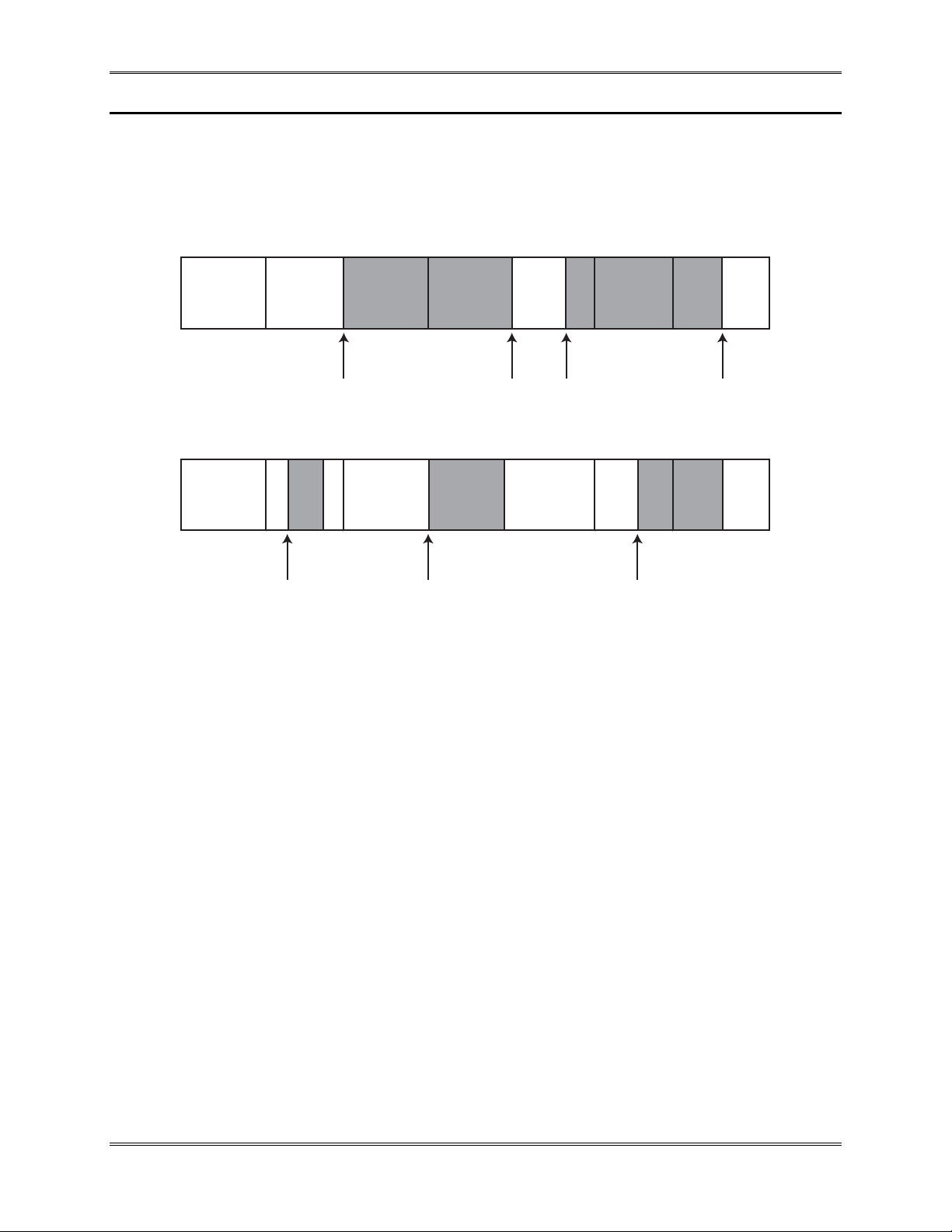
t
l
r
s
1. Introduction to the TriFlash with SD Interface
The SanDisk TriFlash is a very small, flash storage device, designed specifically for storage applications that put a
premium on small form factor, low power and low cost. Flash is the ideal storage medium for portable, batterypowered devices. It features low power consumption and is non-volatile, requiring no power to maintain the stored
data. It also has a wide operating range for temperature, shock and vibration.
TriFlash is well suited to meet the needs of small, low power, electronic devices. With a form factor as small as 10
mm by 12 mm and 1.1 mm thick, TriFlash is expected to be used in a wide variety of portable devices like mobile
phones, pagers, and voice recorders.
To support this wide range of applications, the TriFlash is offered with either the MultiMediaCard (see TriFlash
with MultiMediaCard Interface Product Manual) or Secure Digital (SD) interface. The SD interface product is fully
compatible with SD cards, provides a 4-bit data bus for maximum performance, and, optionally, has the full SD
security features. For compatibility with existing controllers, the TriFlash offers, in addition to these interfaces, an
alternate communication protocol based on the SPI standard.
These interfaces allow for easy integration into any design, regardless of microprocessor used. All device and
interface configuration data (such as maximum frequency and card identification) are stored on the device.
The TriFlash provides up to 1024 million bits of memory using SanDisk Flash memory chips, which were designed
by SanDisk especially for use in mass storage applications. In addition to the mass storage specific flash memory
chip, the TriFlash includes an intelligent controller, which manages interface protocols, and data storage and
retrieval, as well as Error Correction Code (ECC) algorithms, defect handling and diagnostics, power management
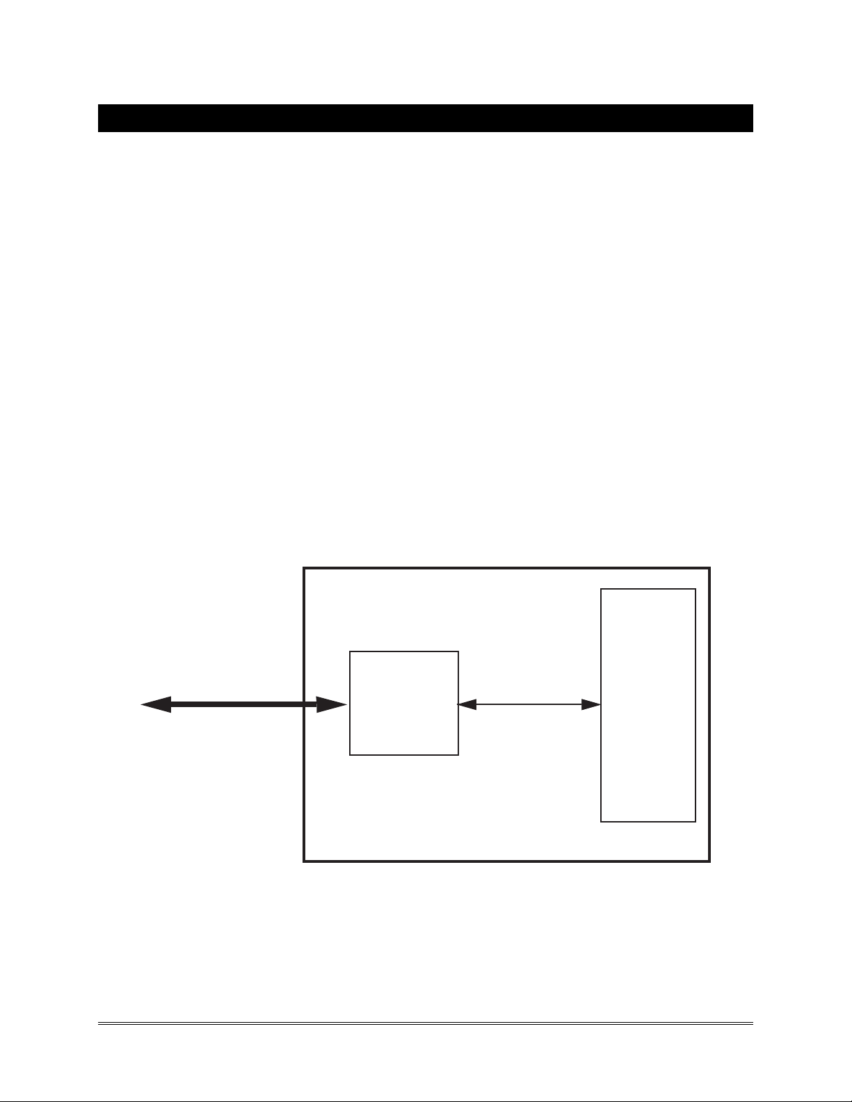
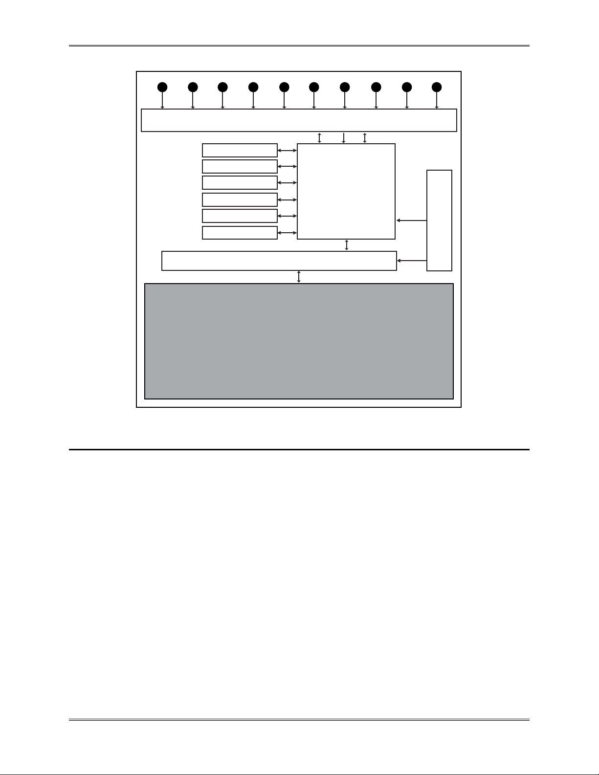
and clock control. Figure 1-1 is a block diagram of the TriFlash with SD Interface.
Data
In/Ou
Contro
Data
Flash
Module
SD Bus/SPI Bus
SanDisk
Single
Chip
Controlle
Interface
SanDisk TriFlash
Figure 1-1. TriFlash with SD Interface Block Diagram
TriFlash with SD Interface Product Manual (Preliminary), Rev. 1.2 © 2002/2003 SANDISK CORPORATION
1-1
Introduction to the TriFlash with SD Interface
1.1. Scope
This document describes the key features and specifications of the TriFlash with SD interface, as well as the
information required to interface this product to a host system.
1.2. Product Models
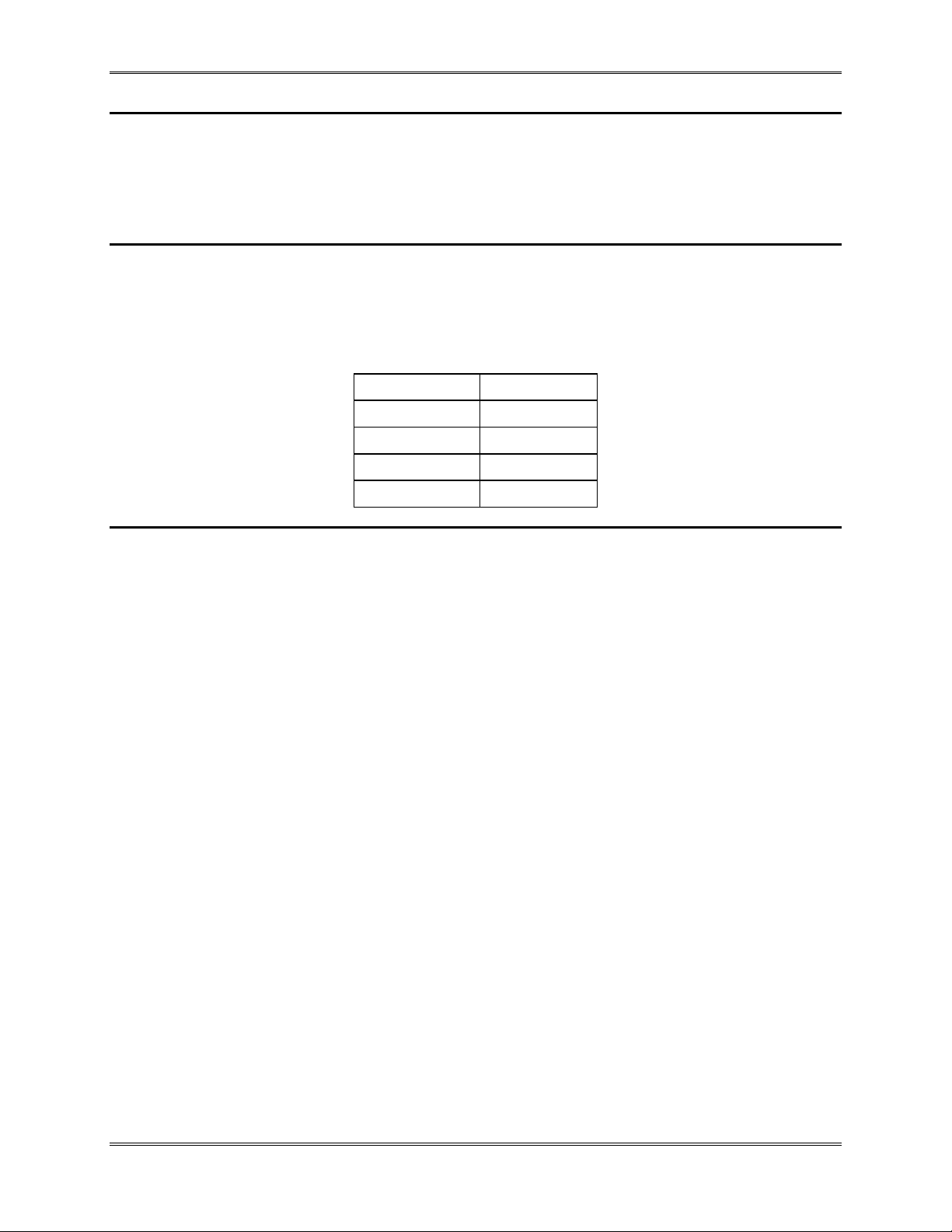
The TriFlash is available in the capacities shown in Table 1-1.
Table 1-1. TriFlash Capacities
SD Model No. Capacities
SDAT2FAH-128 128 Mb
SDBT2FAH-256 256 Mb
SDBT2FCH-512 512 Mb
SDBT2FCH-1024 1024 Mb
1.3. System Features
TriFlash provides the following system features:
• Up to 1024 Mbits of data storage.
• SD Memory Card protocol compatible.
• Supports SPI Mode.
• Targeted for portable and stationary applications for secured (copyrights protected) and non-secured
data storage.
• Voltage range:
− Basic communication (CMD0, CMD15, CMD55, ACMD41): 2.0—3.6V.
− Other commands and memory access: 2.7—3.6V.
• Variable clock rate 0—25 MHz.
• Up to 12.5MByte/sec data transfer rate (using 4 parallel data lines).
• Maximum data rate with up to 10 devices or cards.
• Correction of memory field errors.
• Optional Copyrights Protection Mechanism—Complies with highest security of SDMI standard.
• Built-in write protection features (permanent and temporary).
• Application specific commands.
• Comfortable erase mechanism.
• Standard footprint across all capacities.
1-2 TriFlash with SD Interface Product Manual (Preliminary), Rev. 1.2 © 2002/2003 SANDISK CORPORATION
Introduction to the TriFlash with SD Interface
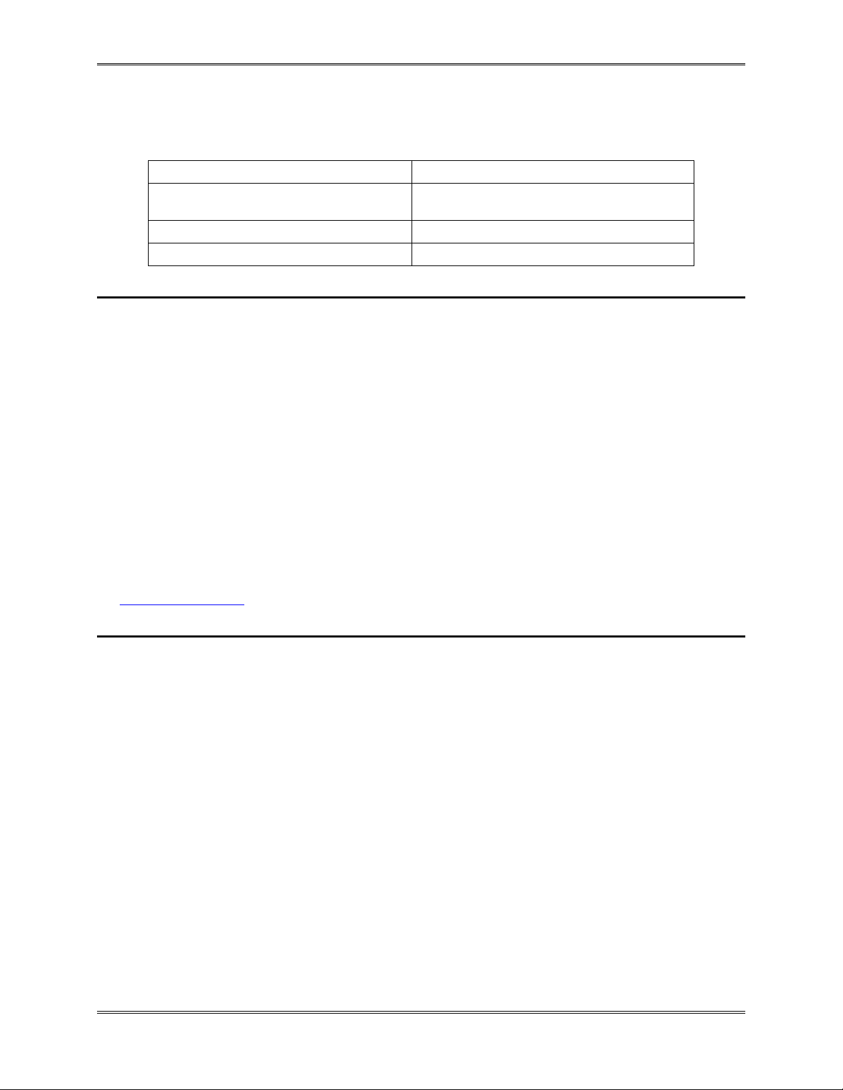
The performance of the communication channel is described in Table 1-2.
Table 1-2. SD Bus/SPI Bus Comparison
TriFlash Using SD Bus TriFlash Using SPI Bus
Six-wire communication channel (clock, command, 4
data lines).
Error-protected data transfer. Optional non-protected data transfer mode available.
Single or multiple block oriented data transfer. Single or multiple block oriented data transfer.
Three-wire serial data bus (Clock, dataIn, dataOut) + card
specific CS signal (hardwired card selection).
1.4. SD Memory Card Standard
The SanDisk TriFlash is fully compatible with the SD Memory Card Physical Layer Specification standard listed
below:
The SD Memory Card Physical Layer System Specification
Version 1.01
This specification may be obtained from:
SD Card Association
53 Muckelemi St.
P.O. Box 189
San Juan Bautista, CA 95045-0189
USA
Phone: 831-623-2107
Fax: 831-623-2248
Email: rcreech@sdcard.org
http://www.sdcard.org
1.5. Functional Description
The SanDisk TriFlash contains a high level, intelligent subsystem as shown in the block diagram, Figure 1-1. This
intelligent (microprocessor) subsystem provides many capabilities not found in other types of devices. These
capabilities include:
• Host independence from details of erasing and programming flash memory.
• Sophisticated system for managing defects (analogous to systems found in magnetic disk drives).
• Sophisticated system for error recovery including a powerful error correction code (ECC).
• Power management for low power operation.
TriFlash with SD Interface Product Manual (Preliminary), Rev. 1.2 © 2002/2003 SANDISK CORPORATION
1-3

Introduction to the TriFlash with SD Interface
1.5.1. Flash Technology Independence
The 512-byte sector size of the TriFlash is the same as that in an IDE magnetic disk drive. To write or read a sector
(or multiple sectors), the host computer software simply issues a Read or Write command to the TriFlash. This
command contains the address. The host software then waits for the command to complete. The host software does
not get involved in the details of how the flash memory is erased, programmed or read. This is extremely important
as flash devices are expected to get more and more complex in the future. Because the TriFlash uses an intelligent
on-board controller, the host system software will not require changing as new flash memory evolves. In other
words, systems that support the TriFlash today will be able to access future SanDisk TriFlash devices built with new
flash technology without having to update or change host software.
1.5.2. Defect and Error Management
The TriFlash contains a sophisticated defect and error management system. This system is analogous to the systems
found in magnetic disk drives and in many cases offers enhancements. For instance, disk drives do not typically
perform a read after write to confirm the data is written correctly because of the performance penalty that would be
incurred. The TriFlash does a read after write under margin conditions to verify that the data is written correctly. In
the rare case that a bit is found to be defective, the TriFlash replaces this bad bit with a spare bit within the sector
header. If necessary, the TriFlash will even replace the entire sector with a spare sector. This is completely
transparent to the host and does not consume any user data space.
The TriFlash device’s soft error rate specification is much better than the magnetic disk drive specification. In the
extremely rare case a read error does occur, the TriFlash has innovative algorithms to recover the data. This is
similar to using retries on a disk drive but is much more sophisticated. The last line of defense is to employ a
powerful ECC to correct the data. If ECC is used to recover data, defective bits are replaced with spare bits to
ensure they do not cause any future problems.
These defect and error management systems coupled with the solid-state construction give the TriFlash unparalleled
reliability.
1.5.3. Endurance
The SanDisk TriFlash has an endurance specification for each sector of 300,000 or 100,000 writes (reading a logical
sector is unlimited) under typical conditions (depending on the model, refer to Table 2-4). This is far beyond what is
needed in nearly all applications of TriFlash devices. Even very heavy use of the TriFlash in cellular phones,
personal communicators, pagers and voice recorders will use only a fraction of the total endurance over the typical
device’s five year lifetime. For instance, it would take over 34 years to wear out an area on the TriFlash on which a
file of any size (from 512 bytes to capacity) was rewritten 3 times per hour, 8 hours a day, 365 days per year.
With typical applications, the endurance limit is not of any practical concern to the vast majority of users.
1.5.4. Wear Leveling
The SanDisk TriFlash does not require or perform a Wear Level operation.
1-4 TriFlash with SD Interface Product Manual (Preliminary), Rev. 1.2 © 2002/2003 SANDISK CORPORATION

Introduction to the TriFlash with SD Interface
1.5.5. Using the Erase Command
The Erase command provides the capability to substantially increase the write performance of the TriFlash. Once a
sector has been erased using the Erase command, a write to that sector will be much faster. This is because a normal
write operation includes a separate sector erase prior to write.
1.5.6. Automatic Sleep Mode
A unique feature of the SanDisk TriFlash (and other SanDisk products) is automatic entrance and exit from sleep
mode. Upon completion of an operation, the TriFlash will enter the sleep mode to conserve power if no further
commands are received within 5 msec. The host does not have to take any action for this to occur. In most systems,
the TriFlash is in sleep mode except when the host is accessing it, thus conserving power.
When the host is ready to access the TriFlash and it is in sleep mode, any command issued to the TriFlash will cause
it to exit sleep and respond.
1.5.7. TriFlash—SD Bus Mode
The following sections provide valuable information for TriFlash in SD Bus Mode.
1.5.7.1. TriFlash Standard Compliance
The TriFlash is fully compliant with the SD Memory Card Physical Layer Standard Specification V1.01. The
structure of the Card Specific Data (CSD) register is compliant with CSD Structure 1.0.
1.5.7.2. Negotiating Operation Conditions
The TriFlash supports the operation condition verification sequence defined in the SD Memory Card Standard
Specifications. Should the TriFlash host define an operating voltage range, which is not supported by the TriFlash,
it will put itself in an inactive state and ignore any bus communication. The only way to get the TriFlash out of the
inactive state is by powering it down and up again.
In addition, the host can explicitly send the TriFlash to the inactive state by using the GO_INACTIVE_STATE
command.
1.5.7.3. Device Acquisition and Identification
The SD bus is a single master (TriFlash host application) and multi-slaves (devices) bus. The Clock and Power lines
are common to all devices on the bus. During the identification process, the host accesses each device separately
through its own command lines. The TriFlash device’s CID register is pre-programmed with a unique card
identification number, which is used during the identification procedure.
TriFlash with SD Interface Product Manual (Preliminary), Rev. 1.2 © 2002/2003 SANDISK CORPORATION
1-5

Introduction to the TriFlash with SD Interface
In addition, the TriFlash host can read the device’s CID register using the READ_CID command. The CID register
is programmed during the TriFlash testing and formatting procedure, on the manufacturing floor. The TriFlash host
can only read this register and not write to it.
An internal pull-up resistor on the DAT3 line may be used for device detection (insertion/removal). The resistor can
be disconnected during data transfer (using ACMD42).
1.5.7.4. Device Status
The device status is separated into two fields: CardStatus and SD_Status.
• CardStatus is stored in a 32 bit status register which is sent as the data field in the card response to
host commands. Status register provides information about the device’s current state and completion
codes for the last host command. The card status can be explicitly read (polled) with the
SEND_STATUS command.
• SD_Status is stored in 512 bits, which are sent as a single data block after it was requested by the host
using the SD_STATUS (ACMD13) command. SD_STATUS contains extended status bits that relate
to BUS_WIDTH, security related bits and future specific applications.
1.5.7.5. Memory Array Partitioning
The basic unit of data transfer to/from the TriFlash is one byte. All data transfer operations which require a block
size always define block lengths as integer multiples of bytes. Some special functions need other partition
granularity.
For block-oriented commands, the following definition is used:
• Block—The unit that is related to the block oriented read and write commands. Its size is the number
of bytes that will be transferred when one block command is sent by the host. The size of a block is
either programmable or fixed. The information about allowed block sizes and the programmability is
stored in the CSD.
The granularity of the erasable units is in general not the same as for the block-oriented commands:
• Sector—The unit that is related to the erase commands. Its size is the number of blocks that will be
erased in one portion. The size of a sector is fixed for each device. The information about the sector
size (in blocks) is stored in the CSD.
For devices that include write protection, the following definition is used:
• WP Group—The minimal unit that may have individual write protection. Its size is the number of
groups that will be write protected by one bit. The size of a WP-group is fixed for each device. The
information about the size is stored in the CSD.
1-6 TriFlash with SD Interface Product Manual (Preliminary), Rev. 1.2 © 2002/2003 SANDISK CORPORATION
Introduction to the TriFlash with SD Interface
TriFlash
WP Group 0
Sector 1
Block
0
Sector 2
Sector 3
Sector n
WP Group 1
WP Group n
Protected Area (Copyright protection)
Sector 1
Block
0
Block
1
Block
1
Block
2
Block
2
Block
n
Block
n
Sector n
Figure 1-2. Memory Array Partitioning
Table 1-3. Memory Array Structures Summary
Part Number Block Size
(Byte)
SDBT2FCH-1024 512 -- 250, 880
SDBT2FCH-512 512 -- 125,440
SDBT2FAH-256 512 -- 62,720
SDAT2FAH-128 512 -- 31,360
1
All measurements are in units per card.
2
The part of the TriFlash with separate DOS partitioning that includes sectors and blocks. The card write protection mechanism
does not affect this area.
Protected Area
Size (Blocks)
2
1
User Area
(Blocks)
TriFlash with SD Interface Product Manual (Preliminary), Rev. 1.2 © 2002/2003 SANDISK CORPORATION
1-7
Introduction to the TriFlash with SD Interface
1.5.7.6. Read and Write Operations
The TriFlash supports two read/write modes as shown in Figure 1-3.
Multiple Block Mode
Memory
Sectors
Memory
Sectors
Memory
Sectors
Address
Start
Memory
Sectors
Memory
Sectors
Memory
Sectors
Stop StopStart
Memory
Sectors
ReadWrite
Memory
Sectors
Single Block Mode Misalignment Error
Memory
Sectors
Start
Address
(Read)
Memory
Sectors
Memory
Sectors
Start
Address
(Write)
Memory
Sectors
Figure 1-3. Data Transfer Formats
Memory
Sectors
Start
Address
(Read/Write)
Memory
Sectors
Single Block Mode
In this mode the host reads or writes one data block in a pre-specified length. The data block transmission is
protected with 16-bit CRC, which is generated by the sending unit and checked by the receiving unit.
The block length, for read operations, is limited by the device sector size (512 bytes) but can be as small as a single
byte. Misalignment is not allowed. Every data block must be contained in a single physical sector.
The block length for write operations must be identical to the sector size and the start address aligned to a sector
boundary.
Multiple Block Mode
This mode is similar to the single block mode, but the host can read/write multiple data blocks (all have the same
length), which will be stored or retrieved from contiguous memory addresses starting at the address specified in the
command.
The operation is terminated with a stop transmission command.
Misalignment and block length restrictions apply to multiple blocks as well and are identical to the single block
read/write operations.
1-8 TriFlash with SD Interface Product Manual (Preliminary), Rev. 1.2 © 2002/2003 SANDISK CORPORATION

Introduction to the TriFlash with SD Interface
1.5.7.7. Data Transfer Rate
The TriFlash can be operated using either a single data line (DAT0) or four data lines (DAT0-DAT3) for data
transfer. The maximum data transfer rate for a single data line is 25 Mb per second and for four data lines it is 100
Mb (12.5 MB) per second.
1.5.7.8. Data Protection
Every sector is protected with an Error Correction Code (ECC). The ECC is generated (in the memory card) when
the sectors are written and validated when the data is read. If defects are found, the data is corrected prior to
transmission to the host.
1.5.7.9. Erase
The smallest erasable unit in the TriFlash is a sector. In order to speed up the erase procedure, multiple sectors can
be erased at the same time.
To facilitate selection, a first command with the starting address is followed by a second command with the final
address, and all sectors within this range will be selected for erase.
1.5.7.10. Write Protection
Two device level write protection options are available: permanent and temporary. Both can be set using the
PROGRAM_CSD command (see below). The permanent write protect bit, once set, cannot be cleared. This feature
is implemented in the TriFlash controller firmware and not with a physical OTP cell.
1.5.7.11. Optional Copyright Protection
A detailed description of the optional Copyright Protection mechanism and related security commands can be found
in the SD Memory Card Security Specification document from the SD Card Association. All TriFlash security
related commands operate in the data transfer mode.
As defined in the SDMI specification, the data content that is saved in the device is saved already encrypted and it
passes transparently to and from the device. No operation is done on the data and there is no restriction to read the
data at any time. Associated with every data packet (song, for example) that is saved in the unprotected memory
there is a special data that is saved in a protected memory area. For any access (any Read, Write or Erase command)
from/to the data in the protected area. For an authentication procedure is done between the TriFlash and the
connected device, either the LCM (PC for example) or the PD (portable device, such as SD player). After the
authentication process passes, the TriFlash is ready to accept or give data from/to the connected device. While the
TriFlash is in the secured mode of operation (after the authentication succeeded) the argument and the associated
data that is sent to the TriFlash or read from the TriFlash are encrypted. At the end of the Read, Write or Erase
operation, the TriFlash automatically gets out of its secured mode.
TriFlash with SD Interface Product Manual (Preliminary), Rev. 1.2 © 2002/2003 SANDISK CORPORATION
1-9

Introduction to the TriFlash with SD Interface
1.5.7.12. Copy Bit
The content of a TriFlash can be marked as an original or a copy using the copy bit in the CSD register. Once the
Copy bit is set (marked as a copy) it cannot be cleared. The Copy bit of the TriFlash is programmed (during test and
formatting on the manufacturing floor) as a copy. The TriFlash can be purchased with the copy bit set (copy) or
cleared, indicating the TriFlash is a master. This feature is implemented in the TriFlash controller firmware and not
with a physical OTP cell.
1.5.7.13. The CSD Register
All the configuration information of the TriFlash is stored in the CSD register. The MSB bytes of the register
contain manufacturer data and the two least significant bytes contain the host controlled data, the card Copy, write
protection and the user file format indication.
The host can read the CSD register and alter the host controlled data bytes using the SEND_CSD and
PROGRAM_CSD commands.
1.5.8. TriFlash—SPI Mode
The SPI mode is a secondary communication protocol for TriFlash devices. This mode is a subset of the SD Bus
protocol, designed to communicate with an SPI channel, commonly found in Motorola’s (and lately a few other
vendors’) microcontrollers.
1.5.8.1. Negotiating Operating Conditions
The operating condition negotiation function of the SD Bus is supported differently in SPI mode by using the
READ_OCR (CMD58) command. The host shall work within the valid voltage range (2.7 to 3.6 volts) of the device
or put the device in an inactive state by sending a GO_INACTIVE command to the device.
1.5.8.2. Card Acquisition and Identification
The host must know the number of devices currently connected on the bus. Specific device selection is done via the
CS signal. The internal pull-up resistor on the CD line may be used for device detection (insertion/removal).
1.5.8.3. Card Status
In SPI mode, only 16 bits (containing the errors relevant to SPI mode) can be read out of the 32-bit TriFlash status
register. The SD_STATUS can be read using ACMD13, the same as in SD Bus mode.
1.5.8.4. Memory Array Partitioning
Memory partitioning in SPI mode is equivalent to SD Bus mode. All read and write commands are byte addressable
with the limitations given in section 1.5.7.5 above.
1-10 TriFlash with SD Interface Product Manual (Preliminary), Rev. 1.2 © 2002/2003 SANDISK CORPORATION

Introduction to the TriFlash with SD Interface
1.5.8.5. Read and Write Operations
In SPI mode, both single and multiple block data transfer modes are supported.
1.5.8.6. Data Transfer Rate
In the SPI mode, only one data line is used for each direction. The SPI mode data transfer rate is the same as the SD
Bus mode data transfer rate when using one data line only (up to 25Mbits per second).
1.5.8.7. Data Protection in the TriFlash
Same as for the SD Bus mode.
1.5.8.8. Erase
Same as in SD Bus mode.
1.5.8.9. Write Protection
Same as in SD Bus mode.
TriFlash with SD Interface Product Manual (Preliminary), Rev. 1.2 © 2002/2003 SANDISK CORPORATION
1-11

Introduction to the TriFlash with SD Interface
This page intentionally left blank.
1-12 TriFlash with SD Interface Product Manual (Preliminary), Rev. 1.2 © 2002/2003 SANDISK CORPORATION
2. Product Specifications
For the specifications in the following sections, values are defined at ambient temperature and nominal supply
voltage unless otherwise stated.
2.1. System Environmental Specifications
Table 2-1. System Environmental Specifications
Temperature Operating:
Humidity Operating:
ESD Protection ± 2kV, Human body model
Vibration Operating:
Shock Operating:
Altitude (relative to sea level) Operating:
2.2. Typical Power Requirements
Table 2-2. Power Requirements
VDD (ripple: max, 60 mV peak to peak) 2.7 V—3.6 V
(Ta = -25 – 85C)
@ VDD = 2.7V @ VDD = 3.6V
Operating current (maximum rates)
Fclk = 25 MHz, 0.5 Mbyte/s
Read/Write speed
Non-Operating:
Non-Operating:
Non-Operating:
Non-Operating:
Non-Operating:
Read: 30 mA
Write: 35 mA
-25° C to 85° C
-40° C to 85° C
8% to 95%, non-condensing
8% to 95%, non-condensing
15 G peak to peak max.
15 G peak to peak max.
1,000 G max.
1,000 G max.
80,000 feet max.
80,000 feet max.
Read: 40 mA
Write: 45 mA
(Ta = -25 – 85C)
Typical Maximum
@ 2.7 V 40 uA 120 uA
Sleep Current
@3.3 V 50 uA 150 uA
TriFlash with SD Interface Product Manual (Preliminary), Rev. 1.2 © 2002/2003 SANDISK CORPORATION
2-1
Product Specifications
2.3. System Performance
Table 2-3. System Performance1
Typical Maximum
Block Read Access Time 1.5 msec 100 msec
CMD1 to Ready (after power up) 50 msec 100 msec
Sleep to Ready 1 msec 2 msec
2.4. System Reliability and Maintenance
Table 2-4. System Reliability and Maintenance Specifications
MTBF > 1,000,000 hours
Preventive Maintenance None
Data Reliability < 1 non-recoverable error in 1014 bits read
Endurance
SDxT2FAH-xxx ≥ 300,000 erase/program cycles per block typical
Endurance
SDxT2FCH-xxx ≥ 100,000 erase/program cycles per block typical
1
All values quoted are under the following conditions:
a) Voltage range: 2.7 V to 3.6 V.
b) Temperature range: -25° C to 85° C.
c) Are independent of the TriFlash clock frequency.
2-2 TriFlash with SD Interface Product Manual (Preliminary), Rev. 1.2 © 2002/2003 SANDISK CORPORATION
Product Specifications
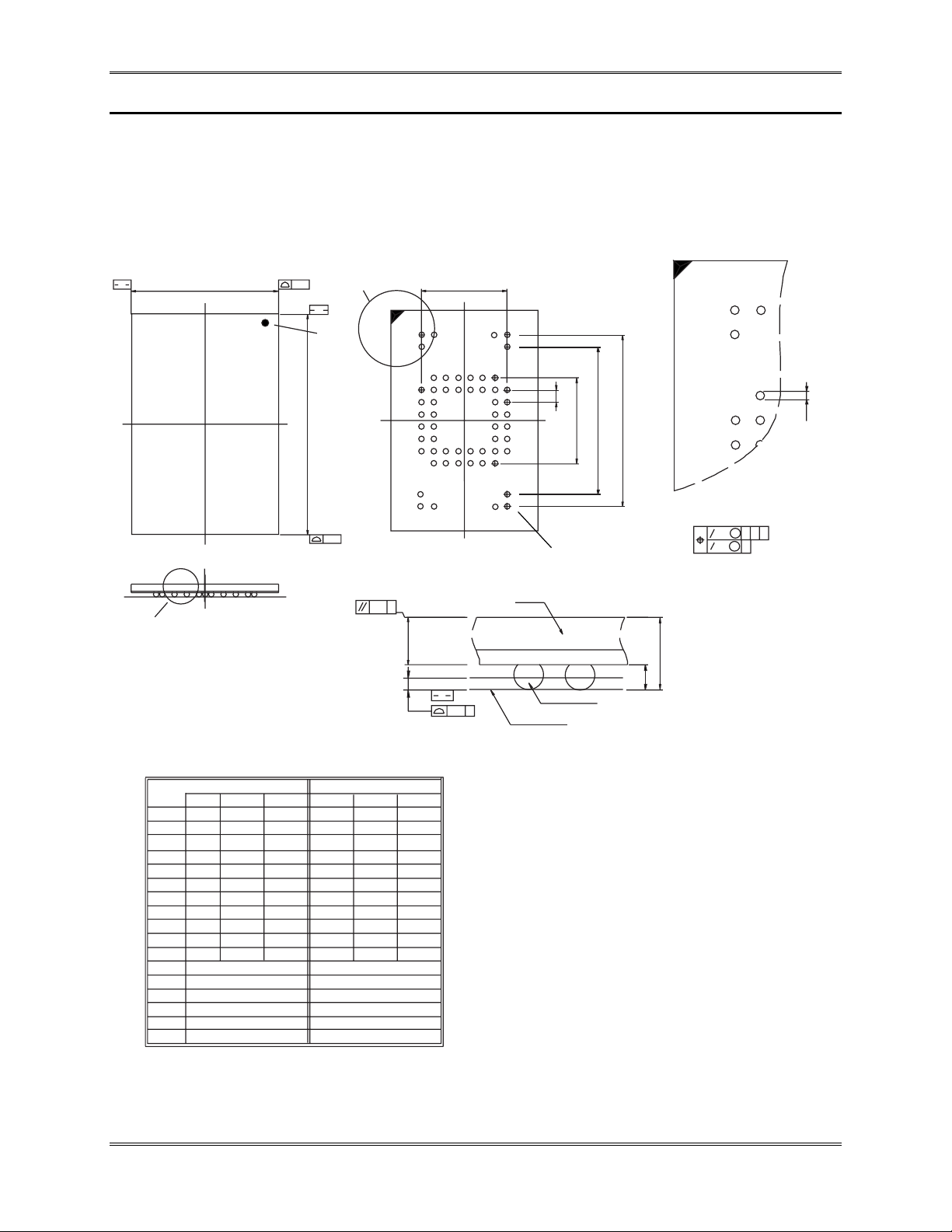
2.5. Physical Specifications
The SanDisk TriFlash is a 44- and 56-pin Thin Fine-Pitched Ball Grid Array (TFBGA). See Figure 2-1 (56-pin) and
Figure 2-2 (44-pin) for the physical specifications and dimensions. See Figure 2-3 for a top view of the pin
definitions.
A B
A
E
aaa
"B"
B
E1
A1
(NOTE 6)
1
2
3
D
4
5
6
7
8
aaa
bbb C
"A"
Dimension in mm Dimension in inch
Symbol MIN NOM MAX Min NOM MAX
A --- --- 1.10 --- --- 0.043
A1 0.32 0.35 0.38 0.013 0.014 0.015
A2 0.62 0.67 0.72 0.024 0.026 0.028
D 17.90 18.00 18.10 0.705 0.709 0.713
E 11.90 12.00 12.10 0.469 0.472 0.476
D1 --- 7.00 --- --- 0.276 -- D2 --- 11.00 --- --- 0.433 -- D3 --- 13.00 --- --- 0.512 -- E1 --- 7.00 --- --- 0.276 -- e --- 1.00 --- --- 0.039 -- b 0.40 0.45 0.50 0.016 0.018 0.020
aaa 0.10 0.004
bbb 0.10 0.004
ddd 0.15 0.006
eee 0.25 0.010
fff 0.10 0.004
MD/ME 12/11 12/11
Figure 2-1. TriFlash Physical Specifications—18 X 12mm Package
ABCDEFGH
A2
C
ddd C
e
D1D3D2
1
2
3
(NOTE 3)
DETAIL: B
C A B
Oeee M
O fff M
Non-functional
C
balls (12 places)
Cavity
A
A1
Solder Ball
Seating Plane
(NOTE 2)
DETAIL: A
NOTE:
1. Controlling Dimension: Millimeter.
2. Primary Datum C and seating plane are defined by the
spherical crowns of the solder balls.
3. Dimensions b is measured at the maximum solder ball
diameter, parallel to Primary Datum C.
4. There shall be a minimum clearance of 0.25mm between
the edge of the solder ball and the body edge.
5. Reference document: JEDEC MO-205.
6. The pattern of Pin 1 Fiducial is for reference only.
7. All numbers are in mm.
8. All numbers are typical unless otherwise stated.
b
TriFlash with SD Interface Product Manual (Preliminary), Rev. 1.2 © 2002/2003 SANDISK CORPORATION
2-3
Product Specifications
A1
H
G
F
E
D
C
B
A
A
"A"
"B"
D
D1
e
12345678
aaa
B
bbb C
E
aaa
A2
C
ddd C
Cavity
A
A1
Solder Ball
Seating Plane
(NOTE 2)
DETAIL: A
C A B
Oeee M
O fff M
C
B
b
A
E1
1
(NOTE 6)
2
(NOTE 3)
DETAIL: B
Dimension in mm Dimension in inch
Symbol MIN NOM MAX Min NOM MAX
A --- --- 1.10 --- --- 0.043
A1 0.32 0.35 0.38 0.013 0.014 0.015
A2 0.62 0.67 0.72 0.024 0.026 0.028
D 11.90 12.00 12.10 0.469 0.472 0.476
E 9.90 10.00 10.10 0.390 0.394 0.398
D1 --- 7.00 --- --- 0.276 -- E1 --- 7.00 --- --- 0.276 -- e --- 1.00 --- --- 0.039 -- b 0.40 0.45 0.50 0.016 0.018 0.020
aaa 0.10 0.004
bbb 0.10 0.004
ddd 0.15 0.006
eee 0.25 0.010
fff 0.10 0.004
MD/ME 8/8 8/8
Figure 2-2. TriFlash Physical Specifications—12 X 10mm Package
NOTE:
1. Controlling Dimension: Millimeter.
2. Primary Datum C and seating plane are defined by the
spherical crowns of the solder balls.
3. Dimensions b is measured at the maximum solder ball
diameter, parallel to Primary Datum C.
4. There shall be a minimum clearance of 0.25mm between
the edge of the solder ball and the body edge.
5. Reference document: JEDEC MO-205.
6. The pattern of Pin 1 Fiducial is for reference only.
2-4 TriFlash with SD Interface Product Manual (Preliminary), Rev. 1.2 © 2002/2003 SANDISK CORPORATION
Product Specifications
G8
DU
F8
DU
E8
DU
D8
DU
C8
DU
B8
DU
H7
GND
G7
RSTB
F7
DU
E7
DU
D7
DU
C7
DU
B7
DU
A7
GND
H6
VDD
G6
DAT2
B6
DU
A6
VDD
CSB_DAT3
H5
DU
G5
B5
WPSB
A5
DU
H4
DU
G4
CMD
B4
SEL_B
A4
DU
H3
DU
G3
DAT1
B3
SEL_A
A3
DU
H2
GND
G2
DAT0
F2
DU
E2
DU
D2
DU
C2
DU
B2
RDY/BSY
A2
VDD
G1
CLK
F1
VDD
E1
DU
D1
GND
C1
VDD
B1
GND
NOTE: DU=Don't Use.
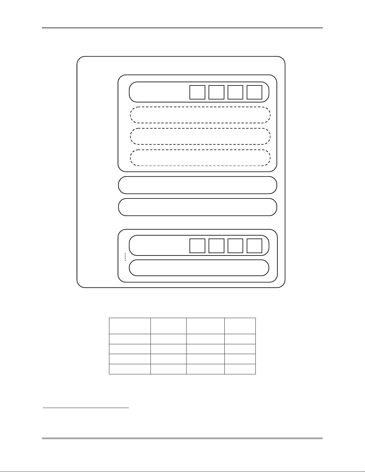
Pin A1 ID
Figure 2-3. TriFlash Pinout (Top View)
TriFlash with SD Interface Product Manual (Preliminary), Rev. 1.2 © 2002/2003 SANDISK CORPORATION
2-5

Product Specifications
This page intentionally left blank.
2-6 TriFlash with SD Interface Product Manual (Preliminary), Rev. 1.2 © 2002/2003 SANDISK CORPORATION
3. TriFlash Interface Description
3.1. General Description of Pins and Registers
The TriFlash is a TFBGA package with 44 core balls (see Figure 2-3). The host is connected to the TriFlash using
the 11 interface connections shown on following 2 tables, plus power and ground balls.
3.1.1. Pin Assignments in SD Bus Mode
Table 3-1. SD Bus Mode Pad Definition
Pin # Name Type1 Function Comment
H6, F1, C1, A2, A6 VDD S Supply Voltage
H7, H2, D1, B1, A7 VSS S Supply Voltage Ground
G2 DAT0 I/O Data Line [Bit 0]
G3 DAT12 I/O Data Line [Bit 1]
G6 DAT2 I/O Data Line [Bit 2]
G5 DAT3 I/O3 Data Line [Bit 3]
G1 CLK I Clock
G4 CMD I/O Command/Response
B5 WPB I Write Protect (Active Low)
G7 RSTB I Reset (Active Low)
B2 RDY/BSY O Ready/Busy Interrupt
B3 SEL_A I Defines I/F Pull up to VDD
B4 SEL_B I Defines I/F Pull up to VDD
1
S=power supply; I=input; O=output using push-pull drivers.
2
The extended DAT lines (DAT1-DAT3) are inputs on power up. They start to operate as DAT lines after the
SET_BUS_WIDTH command.
3
After power up, this line is input with 50KOhm pull-up (can be used for device detection or SPI mode selection). The pull-up
should be disconnected by the user, during regular data transfer, with SET_CLR_CARD_DETECT (ACMD42) command.
TriFlash with SD Interface Product Manual (Preliminary), Rev. 1.2 © 2002/2003 SANDISK CORPORATION
3-1
TriFlash Interface Description
3.1.2. Pin Assignments in SPI Mode
Table 3-2. SPI Bus Mode Pad Definition
H6, F1, C1, A2, A6 VDD S Supply Voltage
H7, H2, D1, B1, A7 VSS S Supply Voltage Ground
G2 DataOut I/O Device to Host Data and Status
G3 DAT1 I/O Unused Pull up to VDD
G6 DAT2 I/O Unused Pull up to VDD
G5 CS I Chip Select (Active low)
G1 CLK I Clock
G4 DataIn I Host to Device Commands and Data
B5 WPB I Write Protect (Active low)
G7 RSTB I Reset (Active low)
B2 RDY/BSY O Ready/Busy Interrupt
B3 SEL_A I Defines I/F Pull up to VDD
B4 SEL_B I Defines I/F Pull up to VDD
3.1.3. Registers
Pin # Name Type
4
Function Comment
Each device has a set of information registers. A detailed description is given in Section 3.5.
Table 3-3. TriFlash Registers
Name Width Description
CID 128 Card identification number: individual card number for identification.
RCA5 16 Relative card address: local system address of a device, dynamically
suggested by the device and approved by the host during initialization.
CSD 128 Card specific data: information about the device operation conditions.
SCR 64 SD Configuration Register: information about the TriFlash’s special
features capabilities.
OCR 32 Operation Condition Register.
The host may reset the devices by switching the power supply off and on again, or toggling the Reset pin. The
device has its own power-on detection circuitry, which puts the device into an idle state after the power-on. The
device can also be reset by sending the GO_IDLE (CMD0) command.
4
S=power supply; I=input; O=output using push-pull drivers.
5
The RCA register is not used (not available) in SPI Mode.
3-2 TriFlash with SD Interface Product Manual (Preliminary), Rev. 1.2 © 2002/2003 SANDISK CORPORATION
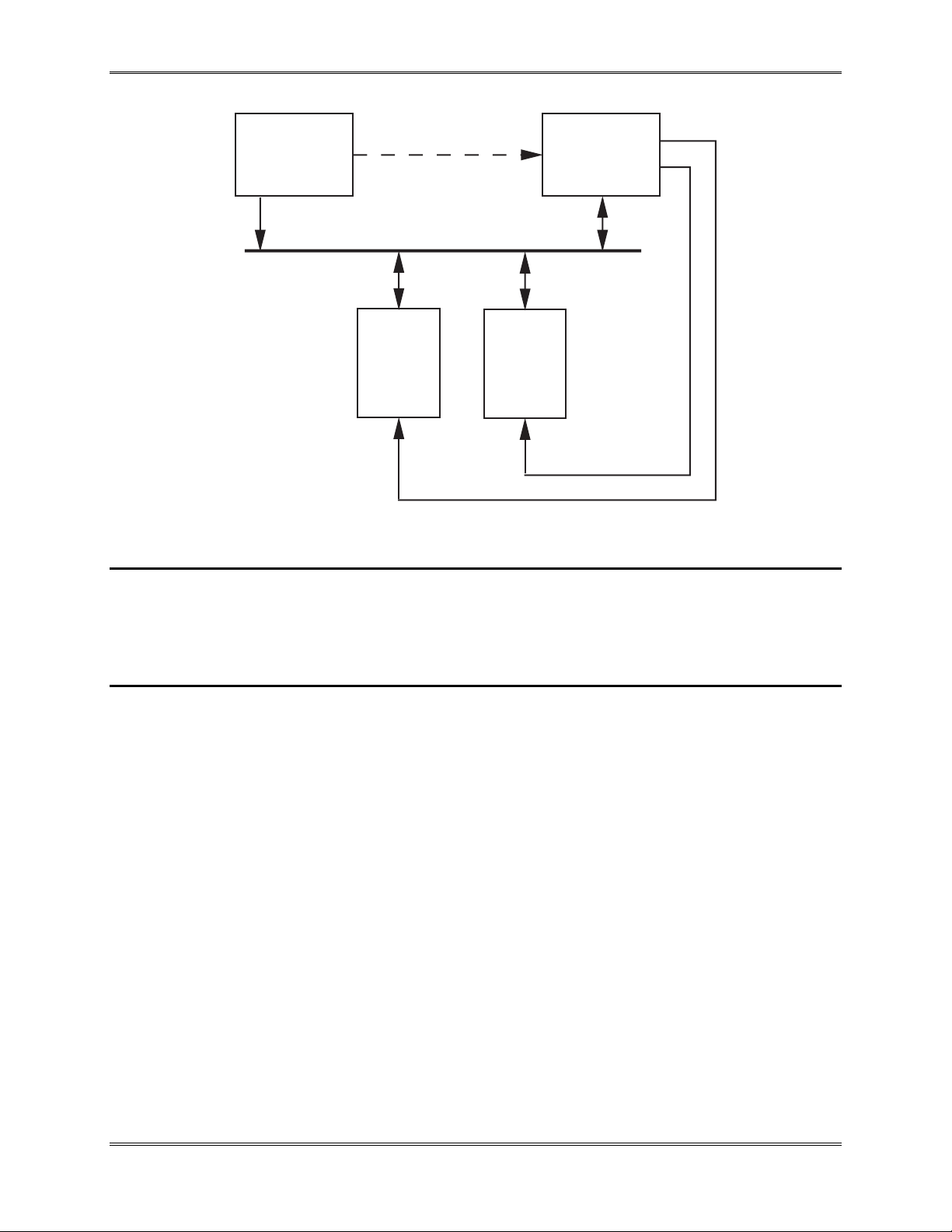
TriFlash Interface Description
DAT2 CD/DAT3 CMD RDY/BSY VDD CLK RSTB WPB DAT0 DAT1
Interface Driver
OCR[31:0]
CID[127:0]
RCA[15:0]
DSR[15:0]
CSD[127:0]
Card Interface
Controller
reset
SCR[63:0]
Memory Core Interface reset
Memory Core
Figure 3-1. TriFlash Architecture
3.2. SD Bus Topology
The SD bus has six communication lines and three supply lines:
• CMD—Command is a bi-directional signal. (Host and device drivers are operating in push pull mode.)
• DAT0-3—Data lines are bi-directional signals. (Host and device drivers are operating in push pull
mode.)
• CLK—Clock is a host to devices signal. (CLK operates in push pull mode.)
• VDD—VDD is the power supply line for all devices.
• VSS—VSS are ground lines.
Power Connection
TriFlash with SD Interface Product Manual (Preliminary), Rev. 1.2 © 2002/2003 SANDISK CORPORATION
3-3
TriFlash Interface Description
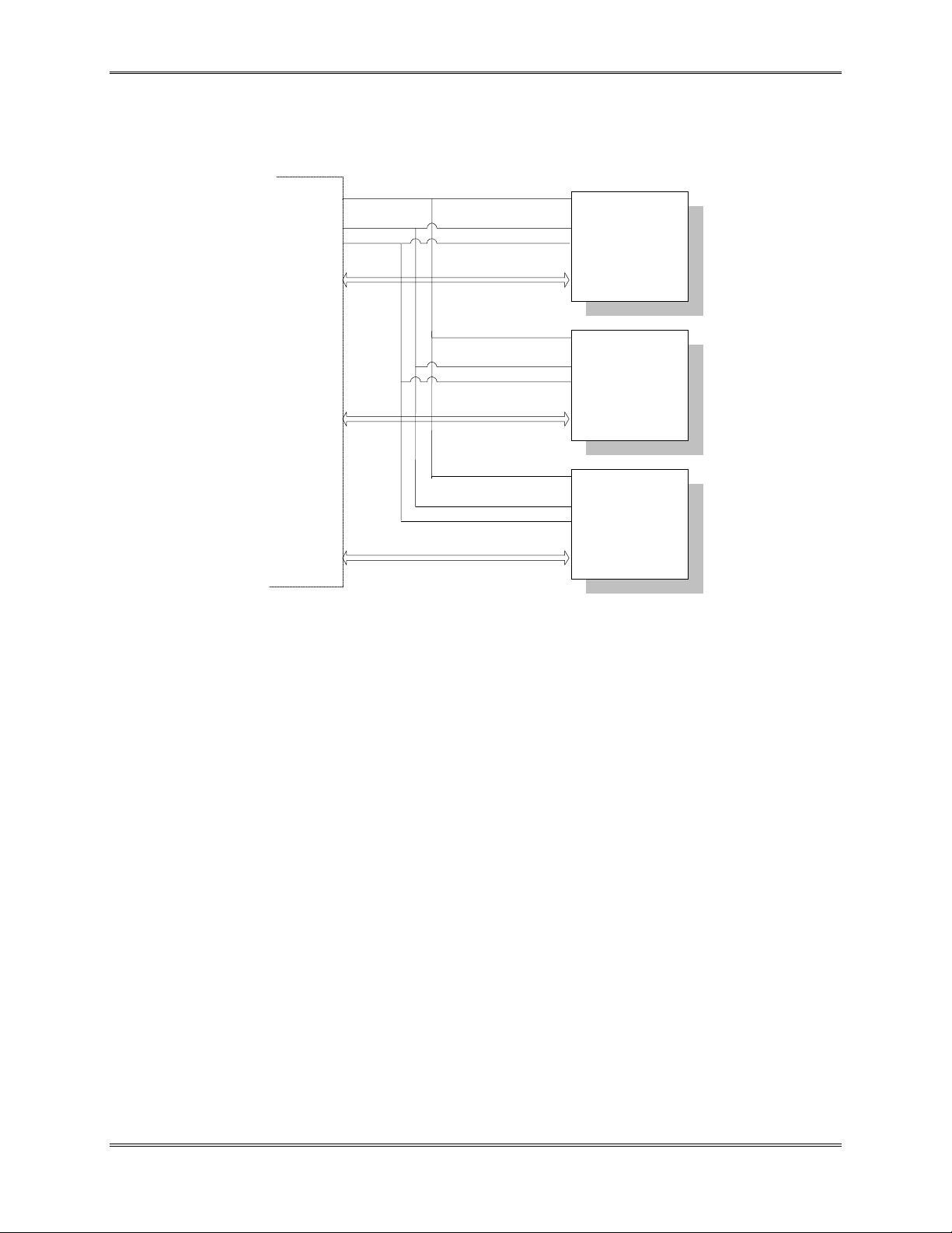
Figure 3-2 shows the bus topology of several devices with one host in SD Bus mode.
HOST
CLK
Vdd
Vss
D0-3(A),
CMD(A)
D0-3(B),
CMD(B)
D0-3(C)
CMD(C)
D0-D3, CMD
D0-D3, CMD
D0, CS, CMD
Figure 3-2. TriFlash System Bus Topology
CLK
Vdd
Vss
CLK
Vdd
Vss
CLK
Vdd
Vss
TriFlash (A)
SD Memory
Card (B)
MultiMediaCard
(C)
D1&D2 Not
Connected
During the initialization process, commands are sent to each device individually, allowing the application to detect
the devices and assign logical addresses to the physical slots. Data is always sent to each device individually.
However, to simplify the handling of the card stack, after initialization, all commands may be sent concurrently to
all devices. Addressing information is provided in the command packet.
The SD Bus allows dynamic configuration of the number of data lines. After power-up, by default, the TriFlash will
use only DAT0 for data transfer. After initialization, the host can change the bus width (number of active data
lines). This feature allows an easy trade off between hardware cost and system performance.
3-4 TriFlash with SD Interface Product Manual (Preliminary), Rev. 1.2 © 2002/2003 SANDISK CORPORATION
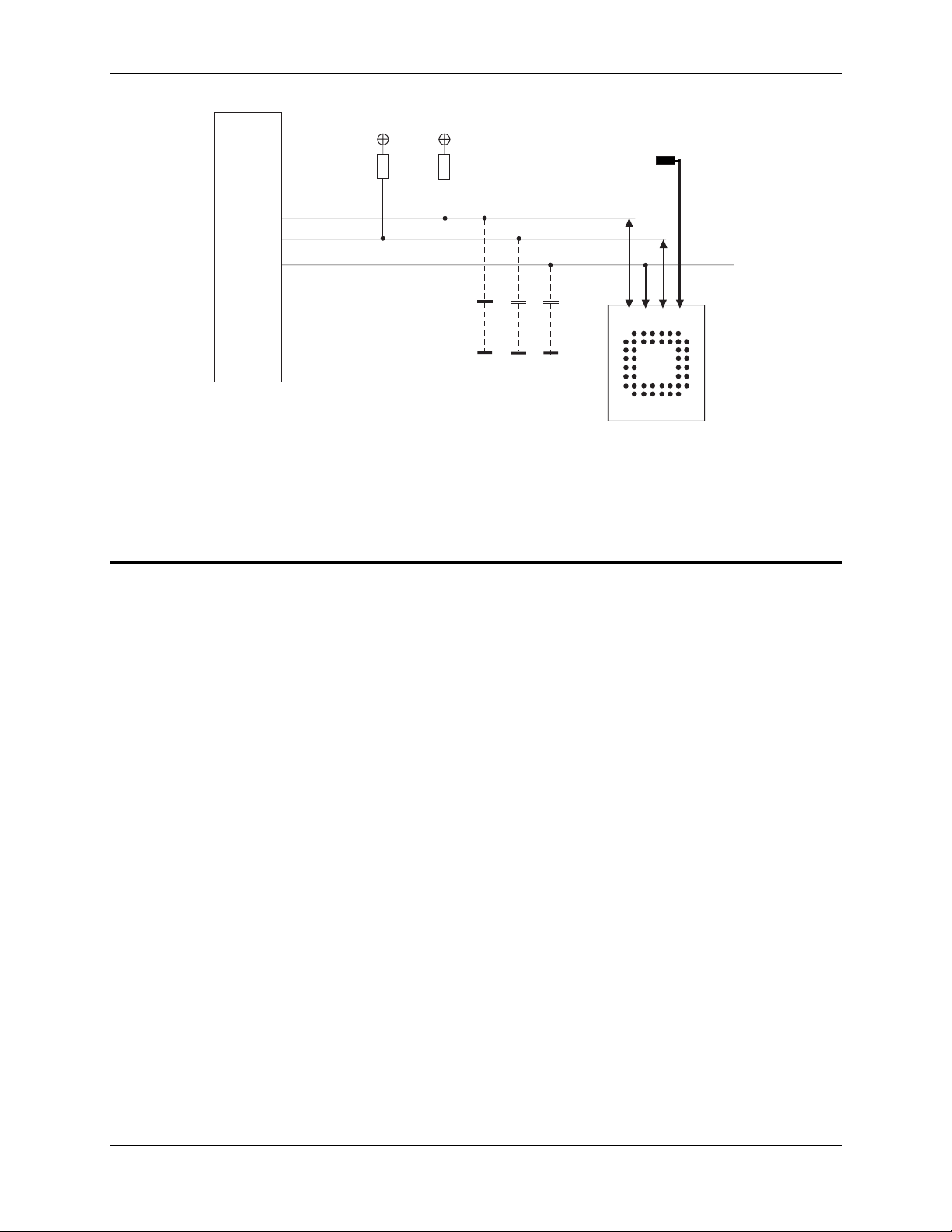
TriFlash Interface Description
V
SS
CLK
TriFlash
Host
R
DAT
R
CM
C1C2C
CMD
DAT 0-3
3
Figure 3-3. SD Bus Circuitry Diagram
and R
R
DAT
are pull-up resistors protecting the CMD and the DAT line against bus floating when all device
CMD
drivers are in a hi-impedance mode. Refer to Table 3-5 for the component values and conditions. C1, C2 and C3 are
the equivalent load capacitance (CL) of each line in the bus.
3.3. SPI Bus Topology
The TriFlash SPI interface is compatible with SPI hosts available on the market. As with any other SPI device the
TriFlash SPI channel consists of the following 4 signals:
• CS—Host to device Chip Select signal.
• CLK—Host to device clock signal
• DataIn—Host to device data signal.
• DataOut—Device to host data signal.
Another SPI common characteristic, which is implemented in the TriFlash as well, is byte transfers. All data tokens
are multiples of 8 bit bytes and always byte aligned to the CS signal.
The SPI standard defines the physical link only and not the complete data transfer protocol. In SPI Bus mode, the
TriFlash uses a subset of the SD protocol and command set.
The TriFlash identification and addressing algorithms are replaced by a hardware Chip Select (CS) signal. A device
(slave) is selected, for every command, by asserting (active low) the CS signal (see Figure 3-4).
The CS signal must be continuously active for the duration of the SPI transaction (command, response and data).
The only exception is device programming time. At this time the host can de-assert the CS signal without affecting
the programming process.
The bi-directional CMD and DAT lines are replaced by uni-directional DataIn and DataOut signals. This eliminates
the ability of executing commands while data is being read or written. An exception is the multi read/write
operations. The Stop Transmission command can be sent during data read. In the multi block write operation a Stop
Transmission token is sent as the first byte of the data block.
TriFlash with SD Interface Product Manual (Preliminary), Rev. 1.2 © 2002/2003 SANDISK CORPORATION
3-5
TriFlash Interface Description
Power
Supply
SPI Bus (CLK, DataIN, DataOut)
TriFlash
Card
Figure 3-4. SPI Bus System
SPI
Card
SPI Bus
Master
CS
CS
3.4. Electrical Interface
The following sections provide valuable information on TriFlash’s electrical interface.
3.4.1. Power-up
The power up of the bus is handled locally in each TriFlash and in the bus master.
3-6 TriFlash with SD Interface Product Manual (Preliminary), Rev. 1.2 © 2002/2003 SANDISK CORPORATION
 Loading...