

Page 1
Chip Resistor
Page 2

Chip Resistor
■
INTRODUCTION
Chip resistors are general passive component which is useful for derating voltage, current
controlling in circuit and surface mounting is available.
Samsung electro mechanics also manufactures a wide range of chip resistors such as general,
precision, trimmable and low ohms and so on.
Production is increasing with demand for small size & light weight of set product. We provide
ultra-small, high-reliability, high-stability resistors.
We have obtained ISO-9002 and QS-9000 certification.
■
FEATURE AND APPLICATION
●
Feature
- Very small, thin, and light weight.
- Both flow and reflow soldering are applicable.
- Owing to the reduced lead inductance, the high frequency characteristic is excellent.
- Suitable size and packaging for surface mount assembly.
- Reel type and Bulk type Packaging are applicable.
●
Application
- General purpose.
- Home Appliances.
(DVD, Digital TV, Camcorder, VTR, Digital Camera, Audio, Tunner)
- For Computers & Communication Devices.
(Notebook, Memory Module, Mobile, Network Equipment, etc)
- 1 -
Page 3
Chip Resistor
■
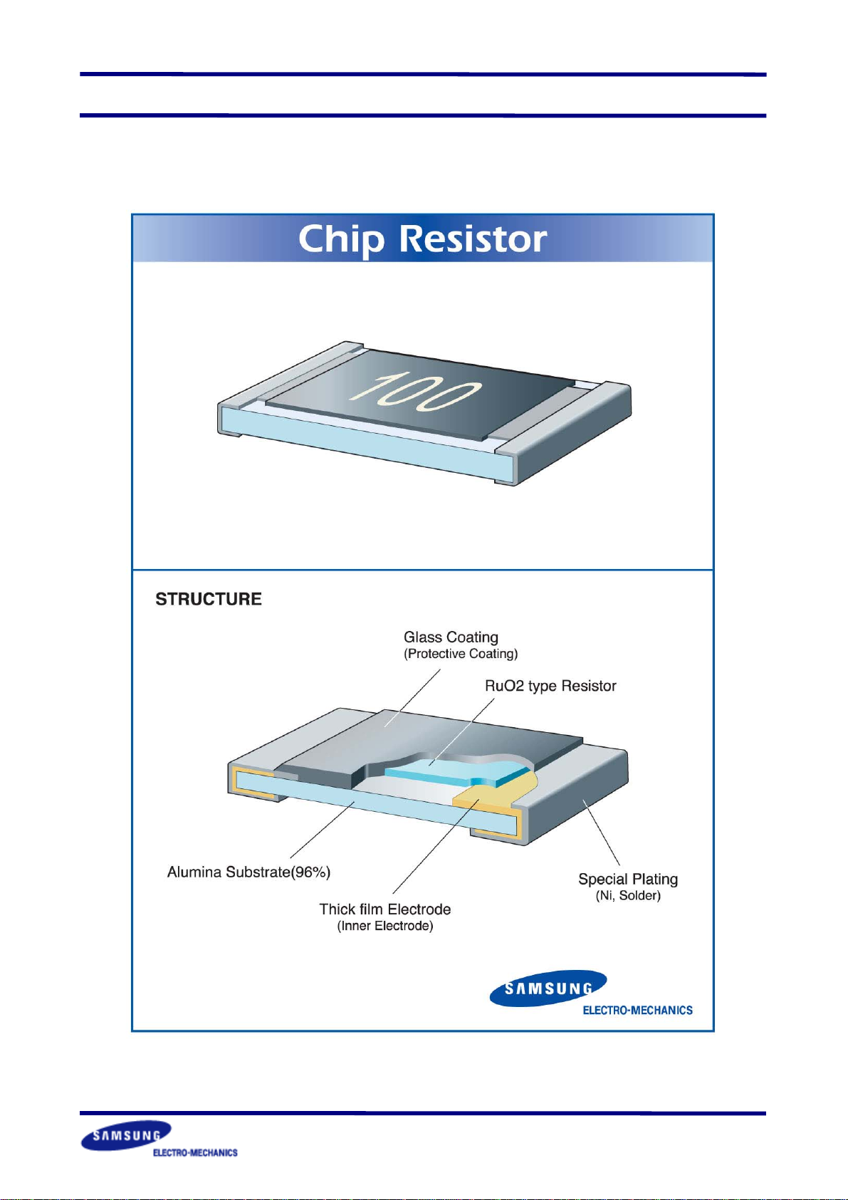
STRUCTURE
- 2 -
Page 4
Chip Resistor
■
APPEARANCE AND DIMENSION
H
l
1
l
2
L
TYPE inch Power (W) L W H I
0603
1005
1608
2012
3216
3225
5025
6432
0201
0402
0603
0805
1206
1210
2010
2512
1/20 0.60±0.03 0.30±0.03 0.23±0.05 0.15±0.05 0.15±0.05 0.16
1/16 1.00±0.05 0.50±0.05 0.35±0.05 0.20±0.10 0.25±0.10 0.6
1/10 1.60±0.10 0.80±0.15 0.45±0.10 0.30±0.20 0.35±0.20 2.1
1/8 2.00±0.20 1.25±0.15 0.50±0.10 0.40±0.20 0.35±0.20 4.9
1/4 3.20±0.20 1.60±0.15 0.55±0.10 0.45±0.20 0.40±0.20 9.5
1/4 3.20±0.20 2.55±0.20 0.55±0.10 0.45±0.20 0.40±0.20 16
1/2 5.00±0.15 2.50±0.15 0.55±0.15 0.60±0.20 0.60±0.20 26
1 6.30±0.15 3.20±0.15 0.55±0.15 0.60±0.20 0.60±0.20 41
W
[Unit:㎜]
1
I
2
Unit
Weight
㎎
㎎
㎎
㎎
㎎
㎎
㎎
㎎
- 3 -
Page 5
Chip Resistor
■
PART NUMBERING
RC 2012 J 100 CS
1
●
1
●
CODE DESIGNATION
RC : This code expresses the Resistor that i s produced by Samsung Electro-Mechanics
CO.LTD. (with the exception of Trimmable Chip Resistor(RT))
2
●
DIMENSION
The dimension is expressed as 4 digits number by SI unit (mm). <Table 1>
Left 2 digits are length of resistor, and the other 2 digits are width. <Fig 1>
2
●
3
●
4
●
5
●
<Fig 1>
<Table 1>
Dimension
(inch)
L
W
H
l
1
l
2
l
1
H
l
L
0603 1005 1608 2012 3216 3225 5025 6432
(0201) (0402) (0603) (0805) (1206) (1210) (2010) (2512)
0.60±0.03 1.00±0.05 1.60±0.10 2.00±0.20 3.20±0.20 3.20±0.20 5.00±0.15 6.30±0.15
0.30±0.03 0.50±0.05 0.80±0.15 1.25±0.15 1.60±0.15 2.55±0.20 2.50±0.15 3.20±0.15
0.23±0.05 0.35±0.05 0.45±0.10 0.50±0.10 0.55±0.10 0.55±0.10 0.55±0.10 0.55±0.10
0.15±0.05 0.20±0.10 0.30±0.20 0.40±0.20 0.45±0.20 0.45±0.20 0.60±0.20 0.60±0.20
0.15±0.05 0.25±0.10 0.35±0.10 0.35±0.20 0.40±0.20 0.40±0.20 0.60±0.20 0.60±0.20
2
W
[Unit:㎜]
- 4 -
Page 6

Chip Resistor
3
●
RESISTANCE TOLERANCE
The Resistance Tolerance is expressed as 1 digit alphabet by EIAJ standard. <Table 2>
<Table 2>
Item F G J K L M
Tolerance (%)
Producing Series E-24, E-96 E-48 E-24 E-12 E-9 E-6
Type P, L G, L G, L G, L, T T T
±
1
±
2
±
5
±
10
±
15
±
Type Representation : G(General), P(Precision), L(Low ohms), T(Trimmable)
4
●
NOMINAL RESISTANCE VALUE
The Nominal Resistance Value is expressed as 3 or 4 digits by EIAJ standard. <Table 3>
<Table 3>
Item 3 Digits mark 4 Digits mark
Resistance
Tolerance
Only number
Number &
alphabet "R"
Example
F, G, J, K, L, M
Left 2 digits : Resistance value
Right 1 digit : Exponential number of 10.
Read alphabet "R" as decimal point.
1) 101 : 10×10
2)7R5:7.5=7.5
3) R75 : 0.75
1
=10×10 = 100
Ω
Ω
Ω
Left 3 digits : Resistance value
Right 1 digit : Exponential number of 10.
Read alphabet "R" as decimal point.
1) 1001 : 100×101= 100×10 = 1
2) 9R09 : 9.09 = 9.09
F, G
Ω
20
㏀
If resistance value in E-96 is same resistance value in E-24, we mark 3 or 4 digits on the
resistor.
In case of JUMPER(0 ohm), '000' is marked on that resistor.
- 5 -
Page 7
Chip Resistor
5
●
PACKAGING CODE
The Packaging Code is expressed as 2 digits alphabet. <Table 4>
<Table 4>
Packaging
Code
CS
ES
AS
GS
Description Dimension Packaging Q'ty
0603, 1005 10,000 PCS
7" REEL PACKAGING
10" REEL PACKAGING 1608, 2012, 3216 10,000 PCS
13" REEL PACKAGING
BULK CASE PACKAGING
1608, 2012, 3216, 3225 5,000 PCS
5025, 6432 4,000 PCS
0603, 1005 40,000 PCS
1608, 2012, 3216, 3225 20,000 PCS
5025, 6432 15,000 PCS
1608 25,000 PCS
2012 10,000 PCS
3216 5,000 PCS
- 6 -
Page 8

Chip Resistor
■
PACKAGING
●
PACKAGING METHOD
Packaging protects the resistor from damage during the shipping or storage.
There are two types of packaging method ; one is "Reel" type, and the other is "Bulk" type.
●
REEL TYPE PACKAGING SPECIFICATION
The packaging specification is based on the EIAJ RC-1009.
<Fig 2> is tape dimension For 0603, 1005 type. <Table 5> is for pocket sizes, A and B.
<Fig 2>
0.5 Max
1.0
Carrier Tape
Top Tape
4.0±0.1
2.0±0.05
0.1
±
1.5
0
B
A
Chip Resistor
1.75±0.1
3.5±0.05
8.0±0.1
0.5 Max
- 7 -
Page 9

Chip Resistor
<Fig 3> is tape dimension For 1608, 2012, 3216, 3225 type. <Table 5> is for pocket sizes,
AandB.
<Fig 3>
1.0 Max
1.0
Carrier Tape
4.0±0.1
2.0±0.05
Top Tape
4.0±0.1 A
Bottom Tape
0.1
0
±
1.5
B
Chip Resistor
1.75±0.1
3.5±0.05
8.0±0.1
1.0 Max
<Fig 4> is tape dimension For 5025, 6432 type. <Table 5> is for pocket sizes, A and B.
<Fig 4>
<Table 5>
Dimension
Symbol
A
B
tMAX=1.1
0603 1005 1608 2012 3216 3225 5025 6432
(0201) (0402) (0603) (0805) (1206) (1210) (2010) (2512)
0.65±0.10 0.70±0.10 1.10±0.20 1.65±0.20 2.00±0.20 2.90±0.20 2.80±0.10 3.50±0.10
1.15±0.10 1.20±0.10 1.90±0.20 2.40±0.20 3.60±0.20 3.60±0.20 5.30±0.20 6.75±0.10
- 8 -
Page 10

Chip Resistor
●
TAPING METHOD
There are empty holes at both start part and end part of carrier tape. <Fig 5>
<Fig 5>
Reel
Empty Portion Chips Empty Portion Lead Part
End
10 Pitches
or more
Packed Part Empty Part Lead Part
Adhesion Tape
*********
5,000 Pitches
or
20,000 Pitches
10 Pitches
or more
200~250 mm
Note
①
The resistor should move in the pocket freely.
②
The resistor should not adhere to the top or bottom tape.
③
There should be no vacant pocket.
④
Peeling strength of the top tape should be within 5g and 80g. <Fig 6>
Start
<Fig 6>
Chip Resistor
Carrier Tape
F
Top Tape
Peeling
°
10
Bottom Tape
- 9 -
Page 11

Chip Resistor
●
REEL DIMENSION
The Reel dimension is classified by the diameter of Reel. <Fig 7> <Table 6>
<Fig 7>
<Table6>
[Unit:mm]
Packaging Code Diameter A B C D
CS 7"
ES 10"
FS,AS 13"
●
BULK TYPE PACKAGING
178
258
330
Φ
70
Φ
80
Φ
80
9.5(13.0)±0.1 1.2±0.1
9.5±0.1 2.0±0.1
9.5±0.1 2.0±0.1
Bulk cassette specification is based on the EIAJ ET-7201. <Fig 8>
The standard packaging quantity depends on the dimension. <Table 7>
<Fig 8>
12
36
11
0
6.0±0.05
4.4±0.05
3.4±0.05
<Table 7>
Dimension Inch Standard packaging quantity Weight (g, avg.)
1608 0603 25,000 PCS 71
2012 0805 10,000 PCS 65
3216 1206 5,000 PCS 67
- 10 -
Page 12

Chip Resistor
●
LABELING
▶
Reel type Label
The reel type label includes following contents as <Fig 9>.
<Fig 9>
- Following -
①
Resistance Value
②
Tolerance, Marking
③
Part Number
④
Quantity
⑤
LOT Number
⑥
Bar-Code
⑦
Serial Number
③
④
⑤
⑥
100 J101
P/N : RC1608J101CS
QTY : 5000PCS
L/N : RMBA20630
①
Ohm
SAMSUNG ELECTRO-MECHANICS CO.,LTD.
②
007
V-2
⑦
▶
Bulk type Label
The bulk type label includes following contents as <Fig 10>.
<Fig 10>
- Following -
①
Part Number
②
Resistance Value
③
LOT Number
④
Quantity
⑤
Bar-Code
⑥
Serial Number
●
BOX PACKAGING METHOD
①
The bulk or reel type packaging is packaged twice by paper box, inner box and outer box.
②
The packaging should protect the resistor from damaging during shipping by vehicle, ship,
airplane and etc.
③
The information of contents is marked on both inner and outer box.
①
②
③
⑤
RC3216J100GS
10 ohm
RC3216J100GS
RMBA71025 ,5000pcs
SAMSUNG ELECTRO-MECHANICS CO.,LTD.
④
10 ohm
00
7
V-2
⑥
※
For other packaging methods, please contact us.
- 11 -
Page 13

Chip Resistor
●
BOX DIMENSION FOR REEL TYPE
①
Max 25,000 pcs ( 5 EA×7" )
30±1.0
185±1.0
185±1.0
③
Max 300,000 pcs ( 60 EA×7" )
215±5.0
②
Max 100,000 pcs ( 20 EA×7" )
195±5.0
66±1.0
285±5.0
(Unit:mm) (Unit:mm)
④
Max 400,000 pcs ( 20 EA×13" )
370±5.0
348±5.0
187±5.0
336±5.0
410±5.0
(Unit:mm)
●
BOX DIMENSION FOR BULK TYPE
①
Inner box ( Cassette×5EA)
41
116
(Unit:mm)
65
339±5.0
②
Outer box ( Inner box×20 EA )
215
242
(Unit:mm)
135
(Unit:mm)
- 12 -
Page 14

Chip Resistor
−
■
RELIABILITY TEST DATA
Jumper's reliability test data are only applied to General type resistor.
●
ELECTRICAL CHARACTERISTIC
The electrical characteristic test should satisfy the test method, procedure, and standard.
If there is no special comment, Each test performs in standard state.
(temperature 20℃, humidity 65%RH, pressure 1023mbar)
item
DC resistance
Temperature
Coefficient
of
Resistance
Permissible deviation
Resistor Jumper
DC resistance value
should be within the
specified resistance
tolerance.
Tolerance ppm/℃Type
100
F
200 L
G Table 9 G, P, L
J Table 9 G, L
K Table 9 G, L
L, M Table 9 G, L, T
<Table 9>
Range(Ω) ppm/
0.1 ≤ R < 1
1≤R<10
10 ≤ R < 1M ±
1M ≤ R < 10M ±
500(L-Type)
+300, -200
200
300
P
℃
Ω
50m
Maximum
-
Test method
묤
Standard : JIS C 5202 (5.1)
묤
Test voltage : <Table 8>
묤
Applying time : within 5 seconds.
묤
Test board : <Fig 11>
<Table 8>
Range (Ω) Voltage (V)
R<1 0.1
R < 10 0.1
10≤R<100 0.3
100≤R<1K 1.0
1K≤R<10K 3.0
10K≤R < 100K 10
100K≤R < 1M 25
1M≤R50
묤
Standard : JIS C 5202 (5.2)
묤
Temp. : 20
묤
Test board : <Fig 11>
묤
Calculation :
TCR(ppm/℃)=
T
R
℃→
℃
20
:20±2
0
:ResistanceatT0(Ω)
0
℃→20℃→
-55
RR
0
RTT
00
℃
℃→
125
1
×
6
10
×
−
T : Test temperature ( -55, 125℃)
R : Resistance at T (Ω)
묤
Standard : JIS C 5202. (5.5)
묤
Test voltage : 2.5 times of rated voltage Max.
surge current at the Jumper.
묤
Applying time : 5 seconds
묤
Test board : <Fig 11>
묤
Standard : JIS C 5202. (5.8)
묤
Test voltage : 2.5 times of rated voltage Max.
surge current at the Jumper.
묤
Test method : 1 sec ON, 25 sec OFF
+400
cycles
묤
Test board : <Fig 11>
10,000
Short time
overload
(STOL)
Intermittent
overload
(IOL)
1. No mechanical
damage
Δ
R should be
2.
within±(1%+0.1Ω)
1. No mechanical
damage
Δ
R should be
2.
within±(3%+0.1Ω)
Ω
50m
Maximum
Ω
50m
Maximum
- 13 -
Page 15

Chip Resistor
item
Withstanding
voltage
Insulation
resistance
Noise
Permissible deviation
Resistor Jumper
묤
No mechanical
damage, short circuit,
or disconnection.
묤
Shouldhavemore
than 1,000M
묤
Noise standard
Ω
<Table 10>
Range (Ω)dBMax.
0.1≤R<1
1≤R < 100
100≤R<1K
1K≤R < 100K
100K≤R<1M
1M≤R < 10M
-10(L-Type)
-10
0
15
20
30
Same as
left
Same as
left
-
Test method
묤
Standard : JIS C 5202. (5.7)
묤
Test voltage : 1005 1608 AC 100V,
others AC 500V
묤
Applying time : 60 +10/-0 seconds
묤
Test board : <Fig 13>
묤
Standard : JIS C 5202. (5.6)
묤
Test voltage : 1005 1608 DC 100V,
others DC 500V
묤
Applying time : 60 seconds
묤
Test pressure : 1.0±0.2 N
묤
Test board : <Fig 13>
묤
Standard : JIS C 5202. (5.9)
JIS appendix1 "Noise measure in
resistor"
묤
Measure equipment : QUAN-TECH NOISE
METER
(MODEL 315C)
●
MECHANICAL CHARACTERISTIC
The mechanical characteristic test should satisfy the test method, procedure, and standard.
If there is no special comment, Each test performs in standard state.
(temperature 20℃, humidity 65%RH, pressure 1023mbar)
item
Solderability
Bending
strength
Permissible deviation
Resistor Jumper
묤
New solder
coated more than
95% of termination
1. No mechanical
damage
Δ
R should be
2.
within±(0.5%+0.05Ω)
Same as
left
Same as
left
Test method
묤
Standard : JIS C 5202. (6.5)
묤
Test temperature : 235±5
묤
Test time : 2±0.5 sec (dipping both side)
묤
Standard : JIS C 5202. (6.1)
묤
Test board : <Fig 12>
묤
Test speed : 100mm/min
묤
Test procedure : press until 3mm,
℃
then keep 5 seconds <Fig 14>
<Fig 14>
20
R205
3
- 14 -
Page 16

Chip Resistor
item
Termination
strength
Withstanding
soldering heat
Vibration
Permissible deviation
Resistor Jumper
묤
No mechanical
damage, or sign of
disconnection
1. No mechanical
damage
Δ
R should be
2.
within±(1%+0.05Ω)
1. No mechanical
damage
Δ
R should be
2.
within±(1%+0.05Ω)
Same as
left
Ω
50m
Maximum
Ω
50m
Maximum
Test method
묤
Standard : JIS C 5202 (6.1)
묤
Test time : applying pressure for 10 seconds
묤
Test tension : 5 N (500g묤f)
1005, 1608 - 3 N (300g묤f)
묤
Standard : JIS C 5202 (6.4)
묤
Temperature : 260±5
묤
Test time : 10±1second (both side dipping)
묤
Test procedure : measures after 24 hours
묤
Standard : JIS C 5202 (6.3)
묤
Test amplitude : 1.5mm
묤
Test procedure : frequency 10Hz - 55Hz -
℃
10Hz each 2 hours in x, y, z direction.
●
ENVIRONMENTAL CHARACTERISTIC
The Environmental characteristic test should satisfy the test method, procedure, and standard.
If there is no special comment, Each test performs in standard state.
(temperature 20℃, humidity 65%RH, pressure 1023mbar)
item
Temperature
cycle
Moisture
resistance life
Permissible deviation
Resistor Jumper
1. No mechanical
damage
Δ
R should be
2.
within±(1%+0.1Ω)
1. No mechanical
damage
Δ
R should be
2.
within <Table 12>
<Table 12>
Range(Ω)
0.1≤R<1
1≤R<10
10≤R<1M
1M≤R < 10M
Δ
±
5%(L-Type)
±
(3%+0.1Ω)
RMAX
±
5%
±
5%
Ω
50m
Maximum
Ω
100m
Maximum
Test method
묤
Standard : JIS C 5202 (7.4)
묤
Test procedure : <Table 11>
묤
Measure : after 5 cycles of procedure
묤
Test board : <Fig 11>
<Table 11>
item 1 2 3 4
temp(℃)-55±2 5~35 125±2 5~35
time(min) 30 15 30 15
묤
Standard : JIS C 5202 (7.9)
묤
Test condition : temp 40±3℃, humid 90 ~
95%RH
묤
Test voltage : rated voltage
묤
Test time : repeat 90min ON, 30min OFF
+48
during 1000
묤
Test board : <Fig 11>
hours
- 15 -
Page 17

Chip Resistor
item
Low
temperature
exposure
High
temperatur
exposure
Load life
Permissible deviation
Resistor Jumper
1. No mechanical
damage
Δ
R should be
2.
within±(3%+0.1Ω)
1. No mechanical
damage
Δ
R should be
2.
within±(3%+0.1Ω)
1. No mechanical
damage
Δ
R should be
2.
within
<Table 13>
<Table 13>
Range(Ω)
0.1≤R<1
1≤R<10
10≤R<1M
1M≤R < 10M
Δ
±
5%(L-Type)
±
(3%+0.1Ω)
RMAX
±
5%
±
5%
Ω
50m
Maximum
Ω
50m
Maximum
Ω
100m
Maximum
Test method
묤
Standard : JIS C 5202 (7.1)
묤
Test temperature : -55±2
묤
Test time : 1000
묤
Measure : after 1 hour
묤
Test board : <Fig 11>
묤
Standard : JIS C 5202 (7.2)
묤
Test temperature : 1608,2012,3216 : 155
묤
Test time : 1000
묤
Measure : after 1 hour
묤
Test board : <Fig 11>
묤
Standard : JIS C 5202 (7.10)
묤
Test temperature : 70±2
묤
Test voltage : rated voltage
묤
Test time : repeat 90min ON, 30min OFF
+48
hours (without load)
2℃, others : 125±2
+48
hours (without load)
during 1000
묤
Test board : <Fig 11>.
+48
℃
℃
hours
±
℃
●
TEST BOARD AND SPECIFICATION
▶
Soldering
▷
The resistor should be fixed on PCB(printed circuit board) for testing.
- Soldering specification : JIS C 5202 (6.2)
* Soldering method : Flow type(Dipping type), Reflow type
* Solder : H63A (JIS Z 3282)
* FLUX : ROSIN 25WT% (JIS K 5902), IPA 75WT% (JIS K 5901)
- Flow soldering condition
* FLUX dipping time : 5∼10 sec
* Pre-treatment : None
* Soldering temp. : 235℃±5
* Soldering time : 5±0.5 sec
* Temp. profile : <Fig 15>
- Reflow soldering condition
* Peak temp. : 230℃±5
* Duration over 220℃:15±5sec
* Solder Cream : Sn-Pb (63-37)
* Temp. Profile : <Fig 16>
℃
℃
- 16 -
Page 18

Chip Resistor
▶
Test board
▷
Test board
<Table 14>
item Dimension (mm)
Dimension Power
0603
1005
1608
2012
3216
3225
5025
1/20W
1/16W
1/10W
1/8W
1/4W
1/4W
1/2W
6432
▷
Bending Test Board
<Table 15>
item Dimension (mm)
Dimension Power
0603
1005
1608
2012
3216
3225
5025
6432
1/20W
1/16W
1/10W
1/8W
1/4W
1/4W
1/2W
1W
1W
a b c f
0.3 1.4 0.3 5.2
0.6 1.9 0.7 4.9
1.0 3.0 1.2 4.5
1.2 4.0 1.65 4.3
2.2 5.0 2.0 3.3
2.2 5.0 2.9 3.3
3.6 7.0 3.0 3.0
5.2 8.0 3.5 2.5
<Table 14>, <Fig 11> are dimensions of test board.
* Board material : epoxy JIS C 6484
* pattern material : pure copper 99.5% or above JIS C 6484
a b c f
0.3 1.4 0.3 5.2
0.6 1.9 0.7 4.9
1.0 3.0 1.2 4.5
1.2 4.0 1.65 4.3
2.2 5.0 2.0 3.3
2.2 5.0 2.9 3.3
3.6 7.0 3.0 3.0
5.2 8.0 3.5 2.5
<Fig 11>
b
<Fig 12>
10 -φ1.0
c
35.08
Connector
58.5
: COPPER PATTERN
:SOLDER-RESISTOR
af d=4.
c
b
100
: COPPER PATTERN
:SOLDER-RESISTOR
3
3.5
f
a
25
5.5
7.5
5
40
<Table 15>, <Fig 12> are dimensions of bending test board.
* Board material : epoxy JIS C 6484
* pattern material : pure copper 99.5% or above JIS C 6484
▶
Sketch of Withstanding voltage and Insulation resistance
<Fig 13>
Cu
P2
V
Cu
Cu
P1P1
Substrate
- 17 -
Page 19

Chip Resistor
■
CHARACTERISTIC GRAPH
●
RESISTANCE RANGE
The Resistance Range that we produce depends on the Dimension and the Resistance
Tolerance of the resistor. <Table 16>
<Table 16>
Dimension
Tolerance
F
G
J
K
L, M
0603 1005 1608 2012 3216 3225 5025 6432
(0201) (0402) (0603) (0805) (1206) (1210) (2010) (2512)
10Ω∼1MΩ10Ω∼1MΩ10Ω∼1MΩ10Ω∼1MΩ10Ω∼1MΩ10Ω∼1MΩ10Ω∼1M
0.1Ω∼1MΩ0.1Ω∼1MΩ0.1Ω∼1MΩ0.1Ω∼1MΩ0.1Ω∼1M
1Ω∼10MΩ1Ω∼10MΩ1Ω∼10MΩ1Ω∼10MΩ1Ω∼10MΩ1Ω∼10MΩ1Ω∼10MΩ1Ω∼10M
10Ω∼1MΩ10Ω∼1MΩ10Ω∼1MΩ10Ω∼1MΩ10Ω∼1MΩ10Ω∼1MΩ10Ω∼1M
0.1Ω∼1MΩ0.1Ω∼1MΩ0.1Ω∼1MΩ0.1Ω∼1MΩ0.1Ω∼1M
1Ω∼10MΩ1Ω∼10MΩ1Ω∼10MΩ1Ω∼10MΩ1Ω∼10MΩ1Ω∼10MΩ1Ω∼10MΩ1Ω∼10M
0.1Ω∼1MΩ0.1Ω∼1MΩ0.1Ω∼1MΩ0.1Ω∼1MΩ0.1Ω∼1M
1Ω∼10MΩ1Ω∼10MΩ1Ω∼10MΩ1Ω∼10MΩ1Ω∼10MΩ1Ω∼10MΩ1Ω∼10MΩ1Ω∼10M
0.1Ω∼1MΩ0.1Ω∼1MΩ0.1Ω∼1MΩ0.1Ω∼1MΩ0.1Ω∼1M
1Ω∼10MΩ1Ω∼10MΩ1Ω∼10MΩ1Ω∼10MΩ1Ω∼10MΩ1Ω∼10M
1Ω∼10MΩ1Ω∼10MΩ1Ω∼10MΩ1Ω∼10MΩ1Ω∼10MΩ1Ω∼10M
Type
Ω
P
Ω
L
Ω
G
Ω
P
Ω
L
Ω
G
Ω
L
Ω
G
Ω
L
Ω
T
Ω
T
Type Representation : G(General), P(Precision), L(Low ohms), T(Trimmable)
- 18 -
Page 20

Chip Resistor
●
RATED POWER
The Rated Power is classified by the dimension of the resistor. <Table 17>
<Table 17>
Dimension
item
Rated Power
Working Volt.(Max.) 25 V 50 V 50 V 150 V 200 V 200 V 200 V 200 V
STOL, IOL Volt.(Max.) 50 V 100 V 100 V 300 V 400 V 400 V 400 V 400 V
※
The rated power is specified as continuous full loading power at the ambient temperature of 70
±2℃
.Incaseofthetemperatureexceeding70±2℃, the power should be derated in
0603 1005 1608 2012 3216 3225 5025 6432
(0201) (0402) (0603) (0805) (1206) (1210) (2010) (2512)
1/20 W
(0.05 W)
1/16 W
(0.063 W)
1/10 W
(0.100 W)
1/8 W
(0.125 W)
1/4 W
(0.25 W)
1/4 W
(0.25 W)
1/2 W
(0.5W)
1.0 W
accordance to <Fig 17>.
<Fig 17>
[0603, 1005, 3225, 5025, 6432]
Ratedloadpercent(%)
100
Ambient temperature (℃)
80
[1608, 2012, 3216]
Ratedloadpercent(%)
100
Ambient temperature (℃)
80
60
40
20
-55
0
-40
▶
Working Temperature
-55
-55
04080120
℃∼
+125℃: 0603, 1005, 3225, 5025, 6432
℃∼
+ 155
70
℃
: 1608, 2012, 3216
125
60
40
20
-55
0
0306090 150
-30
70
120
155
- 19 -
Page 21

Chip Resistor
■
APPLICATION MANUAL
●
Applications
Chip resistors are designed for general electronic devices such as home appliances, computer,
mobile communications, digital circuit, etc.
If you require our products with high reliability-performing at more than 125C or below -55C- for
medical equipments, aircraft, high speed machines, military usage, and items that can affect
human life or if you need to use in specific conditions (corrosive gas atmosphere), please contact
us beforehand.
▶
Normal Operation temperature ranges(℃)asfollows.
- 1608, 2012, 3216(general, precision) : -55℃ ~+155℃
- Others (rectangular, array, trimmable) : -55℃ ~+125℃
▶
Although resistor body is coated, sharp excessive impact should be avoided to prevent
damages and adverse effects on characteristics(resistor value, open circuited, T.C.R.).
●
Storage
To maintain proper quality of chip components, the following precautions are required for storage
environment, method and period.
▶
Storage Environment
- Chip components may be deformed, if the temperature of packaged components exceeds
40C.
- Do not store where the soldering properties can be deteriorated by harmful gas such as
sulphurous gas, chlorine gas, etc.
- Bulk packed chip components should be used as soon as the seal is opened, thus
preventing the solderability from deteriorating.
- The remaining unused chips should be put in the original bag and sealed again or store in
a desiccator containing a desiccating agent.
▶
Storage Time Period
- Stored chip components should be used within 12 months after receiving the components.
If 12 months or more have elapsed, please check the solderability before actually using.
●
Mounting
Please give more attention not to press the chip owing to the nozzle's improper height when it
is mounted on PCB.
(Excessive pressure may cause exterior damage, change in resistance, circuit open, etc.)
- 20 -
Page 22

Chip Resistor
●
Soldering
Our products have Ag electrodes protected by double layer.
▶
1st Ni Coating
- This prevents Ag electrode from leaching and enhance the bonding with Sn-Pb.
▶
2nd Sn-Pb Coating
- This is made of Sn 90% and Pb 10% with melting point 213℃ to prevent it from melting
when solder cream melts, and to enhance the bonding.
- Commercial solder creams are made of Sn 63% and Pb 37% with melting point 183℃.
●
Cleaning
After Soldering Cleaning, soldering flux & Ionic cleaning liquid should be avoided on product.
If any possibility on product, please take a test before usage.
●
Caution for chip resistor separation from PCB
Chip resistor installation on PCB is similar phenomenon on chocolate chip on top of cake.
PCB has enough flexibility on outer force but Chip resistor can be defected without any bending.
(By chip resistor use of Ceramic, solder, metal)
Therefore, when separate from Chip resistor on PCB, be ware of any crack of chip
●
Others
▶
Manual work
- Whenever separate chip resistor from PCB, do not re-use the chip resistor for circuit safety.
hip resistor can be electrical specification change by soldering Iron after separation.
C
Re-use of separated chip resistor should be prohibited.
▶
Do not use more than rated voltage.(check the contents on the file)
- 21 -
Page 23

Chip Resistor
■
NOTICE
●
Usage of the resistor
▶
Flow Soldering
After sticking the resistor to PCB with paste, dip the PCB into solder bath. <Fig 15>
<Fig 15>
▶
Reflow Soldering
Temp.
235±5
℃
Δ
T≤150
℃
Pre-heating
Soldering Cooling
within 5 sec
After printing solder c reams on PCB, place the resistor on the solder cream.
Then heat the PCB. <Fig 16>
<Fig 16>
Temp.
230±5
200
160
℃
℃
℃
Peak temp.
within 10 sec
Time
℃
130
●
Caution
▶
Storage condition
Pre-heating
within 120 sec
Soldering
within 20 sec
Cooling
Please make sure that keep the storage conditions.
* Temperature : 5
▶
Damage control
℃∼35℃
,*Humidity:45%RH∼85%RH
Please handle with care, to prevent damaging the resistor.
Specially, the excessive nozzles' height of SMD or the extreme touch with tweezers.
▶
Leaching prevention
It is important to keep the soldering conditions for prevent Ag leaching in Flow soldering.
Time
- 22 -
 Loading...