

Page 1
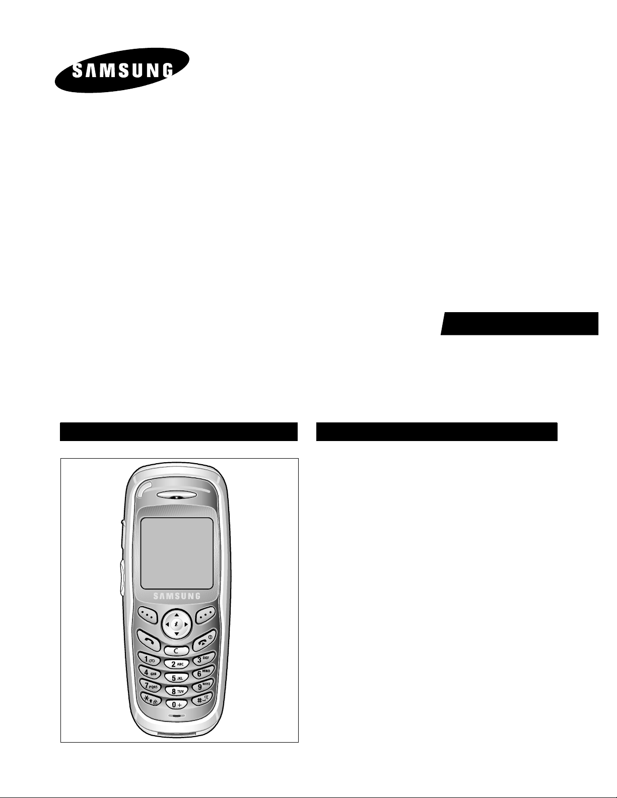
GSM TELEPHONE
SGH-X100
SERVICE
Manual
GSM TELEPHONE CONTENTS
1. Specification
2. Circuit Description
3. Exploded Views and Parts List
4. Electrical Parts List
5. Block Diagrams
6. PCB Diagrams
7. Flow Chart of Troubleshooting
Page 2

ELECTRONICS
This Service Manual is a property of Samsung Electronics Co.,Ltd.
Any unauthorized use of Manual can be punished under applicable
International and/or domestic law.
ⓒ
Samsung Electronics Co.,Ltd. June. 2003
Printed in Korea.
Code No.: GH68-04326A
BASIC.
Page 3
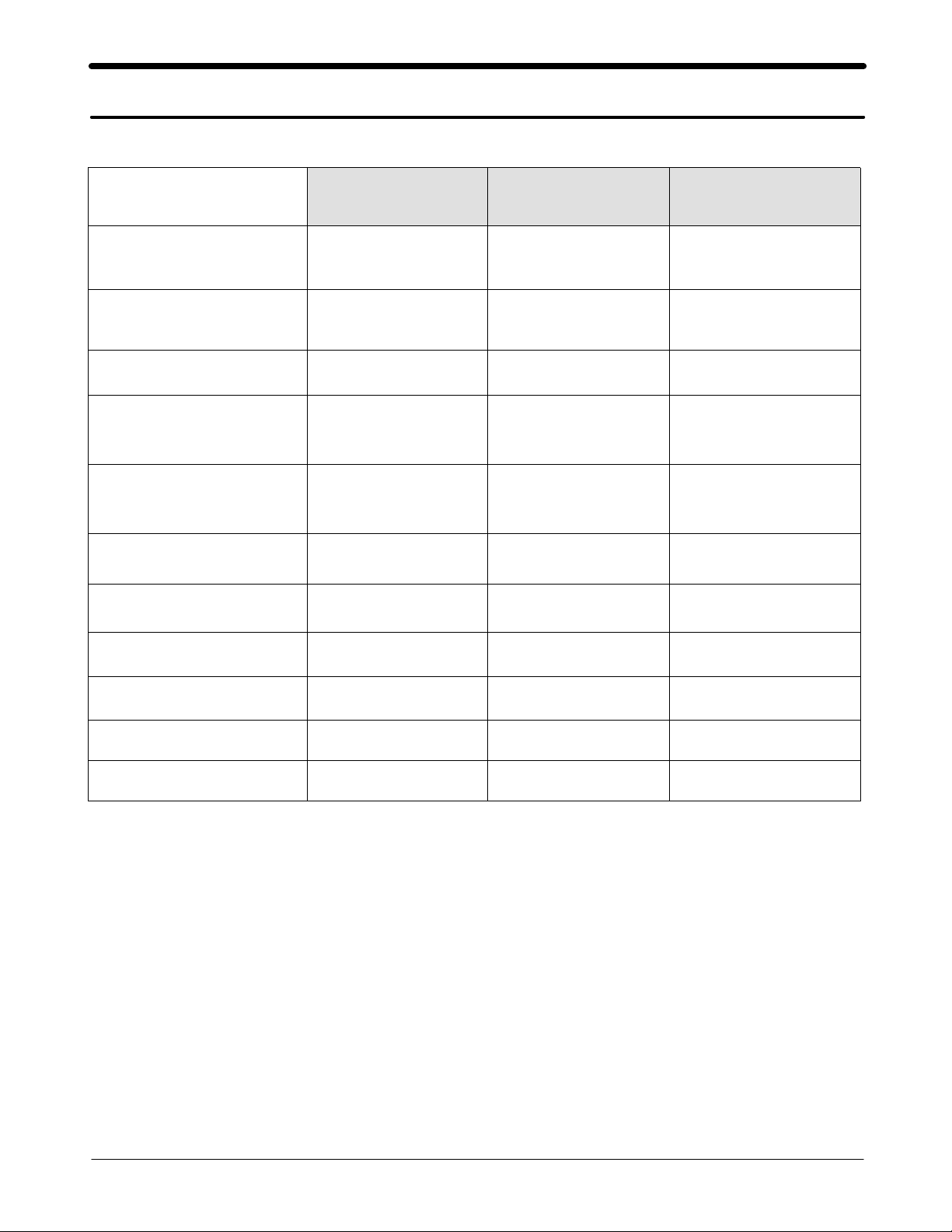
1. SGH-X100 Specification
1. GSM General Specification
GSM900
Phase 1
Freq. Band[MHz]
Uplink/Downlin k
ARFCN range 1~12 4 0~124 & 975~1023 512~885
Tx/Rx spacin g 45MHz 45MHz 95MHz
Mod. Bit rate/
Bit Period
Time Slot Period/Frame
Period
Modulation 0.3GMSK 0.3GMSK 0.3GMSK
MS Power 33dBm~13 dBm 33dBm~5dBm 30dBm~0dBm
890~915
935~960
270.833k bps
3.69 2us
576.9us
4.61 5ms
EGSM 900
Phase 2
880~915
925~960
270.833k bps
3.69 2us
576.9us
4.61 5ms
DCS1800
Phase 1
1710 ~1785
1805 ~1880
270.833k bps
3.69 2us
576.9us
4.61 5ms
Power Class 5pcl ~ 15pcl 5pcl ~ 19pcl 0pcl ~ 15pcl
Sensitivity -102 dBm -102 dBm -100 dBm
TDMA Mux 8 8 8
Cell Rad ius 35Km 35Km 2Km
1-1
SAMSUNG Proprietary-Contents may change without notice
This Document can not be used without Samsung's authorization
Page 4
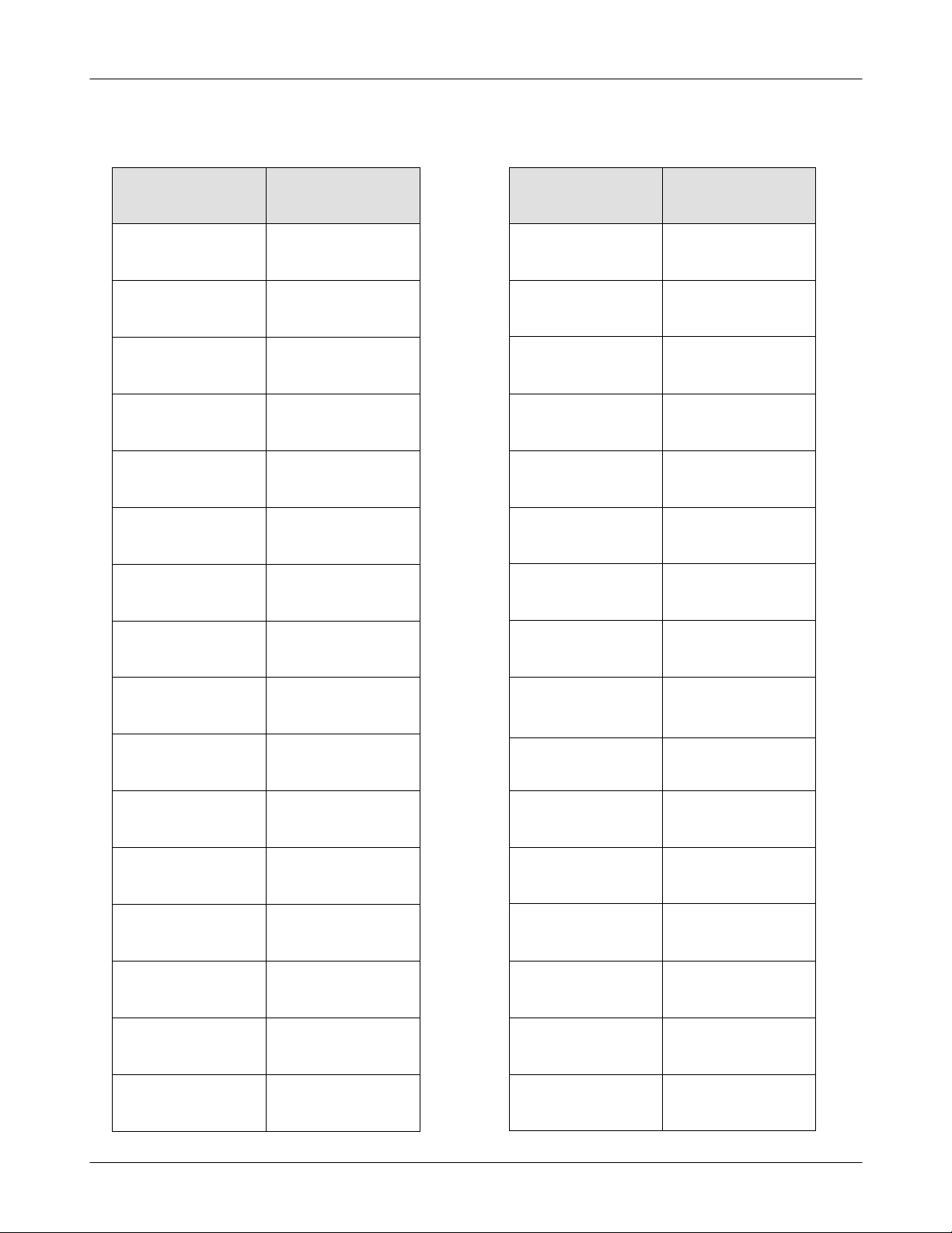
SGH-V200 Specification
2. GSM TX power class
TX Power
control level
5 33±2 dBm
6 31±2 dBm
7 29±2 dBm
8 27±2 dBm
9 25±2 dBm
10 23±2 dBm
11 21±2 dBm
GSM900
TX Power
control level
0 30±3 dBm
1 28±3 dBm
2 26±3 dBm
3 24±3 dBm
4 22±3 dBm
5 20±3 dBm
6 18±3 dBm
DCS1800
12 19±2 dBm
13 17±2 dBm
14 15±2 dBm
15 13±2 dBm
16 11±3 dBm
17 9±3dBm
18 7±3 dBm
19 5±3 dBm
7 16±3 dBm
8 14±3 dBm
9 12±4 dBm
10 10±4 dBm
11 8±4dBm
12 6±4 dBm
13 4±4 dBm
14 2±5 dBm
15 0±5 dBm
1-2
SAMSUNG Proprietary-Contents may change without notice
This Document can not be used without Samsung's authorization
Page 5
2. SGH-X100 Circuit Description
1. SGH-
X100
RF Circuit Description
1) RX PART
1. ASM(U100)→Switching Tx, Rx path for GSM900, DCS1800 by logic controlling.
2. ASM Control Logic (U104, U106)→Truth Table
VC1 VC2
GSM Tx Mode H L
DCS Tx Mode L H
GSM Rx Mode L L
DCS Rx Mode L L
3. FILTER
To convert Electromagnetic Field Wave to Acoustic Wave and then pass the specific frequency band.
- GSM FILTER (F101)→For filtering the frequency band between 925 ~ 960 MHz
- DCS FILTER (F102)→For filtering the frequency band 1805 and 1880 MHz.
4. VC-TCXO (OSC101)
To generate the 26MHz reference clock to drive the logic and RF. After additional process, the reference clock applies to
the U103 Rx IQ demodulator and Tx IQ modulator. The oscillator for RX IQ demodulator and Tx modulator are
controlled by serial data to select channel and use fast lock mode for GPRS high class operation.
5. Transceiver (U103)
The receiver front-end converts the aerial RF signal from EGSM, DCS bands down to a low intermediate frequency (IF)
of 100 kHz. The first stages are symmetrical low noise amplifiers (LNAs). They are matched to 50 ohm. The LNAs are
followed by an I, Q down-mixer. It consists of two mixers in parallel but driven by quadrature out of phase LO signals.
The In phase (I) and Quadrature phase (Q) IF signals are low pass filtered to provide protection from high frequency
offset interferes. The low IF I and Q signals are then fed into the channel filter. The front-end low IF I and Q outputs
enter the integrated bandpass channel filter with provision for five 8 dB gain steps in front of the filter.
2) TX PART
Baseband IQ signal fed into offset PLL, this function is included inside of U103 chip. OSC100 chip generates modulator
signal which power level is about 6.5dBm and fed into Power Amplifier(U101). The PA output power and power ramping
are well controlled by Auto Power Control circuit. We use offset PLL below
GSM -35dBc
DCS -35dBc
GSM -66dBc
DCS -65dBc
GSM -75dBc
DCS -68dBc
Modulation Spectrum
200kHz offset
30 kHz bandwidth
400kHz offset
30 kHz bandwidth
600kHz ~ 1.8MHz offset
30 kHz bandwidth
2-1
SAMSUNG Proprietary-Contents may change without notice
This Document can not be used without Samsung's authorization
Page 6

SGH-X100 Circuit Description
2. Baseband Circuit description of SGH-X100
1) PCF50601
1.1 Power Management
Ten low-dropout regulators designed specifically for GSM applications power the terminal and help ensure optimal system
performance and long battery life. A programmable boost converter provides support for 1.8V, 3.0V, and 5.0V SIMs, while
self-resetting, electronically fused switch supplies power to external accessories. Ancillary support functions, such as RTC
module and High Voltage Charge pump, Clock generator, aid in reducing both board area and system complexity.
I2C BUS serial interface provides access to control and configuration registers. This interface gives a microprocessor full
control of the PCF50601 and enables system designers to maximize both standby and talk times. Supervisory functions.
including a reset generator, an input voltage monitor, and a temperature sensor, support reliable system design. These
functions work together to ensure proper system behavior during start-up or in the event of a fault condition(low
microprocessor voltage, insufficient battery energy, or excessive die temperature).
1.2. Backlight Brightness Modulator
The Backlight Brightness Modulator (BBM) contains a programmable Pulse-width modulator (PWM) and FET to modulate
the intensity of a series of LED or to control a DC/DC converter that drives LCD backlight. This phone (SGH-X100) is
not use PWM, but use DC CONTROL (BACKLIGHT). So "BACKLIGHT" voltage is high value, backlight is bright.
1.3. Clock Generato
The Clock Generator (CG) generates all clocks for internal and external usage. The 32768 Hz crystal oscillator provides an
accurate low clock frequency for the PCF50601 and other circuitry.
r
2) Connector
2-1. LCD Connector
LCD is consisted of main LCD(color 65K STN LCD). Chip select signals in the U304, LCD_CS can enable LCD.
LCD_CS signal is LCD select signal. This signal is from ENABLE part of OM6357.
"RESET_2V8" signal initiates the Reset process of the LCD.
16-bit data lines(HD(0)~HD(15)) transfers data and commands to LCD through by pass capacitor. Data and commands use
"RS" signal. If this signal is high, Inputs to LCD are commands. If it is low, Inputs to LCD are data. The signal which
informs the input or output state to LCD, is required. But this system is not necessary this signal. So "L_WR" signal is
used to write data or commands to LCD. Power signali for LCD is "VDD3".
2-2. Key
This is consisted of key interface pins among OM6357, KBIO(0:7). These signals compose the matrix. Result of matrix
informs the key status to key interface in the OM6357. Power on/off key is seperated from the matrix. So power on/off
signal is connected with PCF50601 to enable PCF50601. Ten key LEDs use the "VDD_KEY" supply voltage.
"VDD_KEY" signal enables LEDs with current control.
2-2
SAMSUNG Proprietary-Contents may change without notice
This Document can not be used without Samsung's authorization
Page 7

2. SGH-X100 Circuit Description
2-3. EMI ESD Filter
This system uses the EMI ESD filter, EMIF09 to protect noise from IF CONNECTOR part.
2-4. IF connetor
It is 18-pin connector. They are designed to use VBAT, V_EXT_CHARGE, TXD0, RXD0, RTS0, CTS0, JIG_REC,
CHARGER_OK, RXD1, TXD1, AUX_MIC, AUX_SPK and GND. They connected to power supply IC, microprocessor and
signal processor IC.
3) Battery Charge Management
a complete constant-current/constant-voltage linear charger for single cell lithium-ion batteries. If ta connected to phone,
"V_EXT_CHARGE" enable charger IC and supply current to battery. when fault condition caused, "CHG_ON" signal level
change low to high and charger IC stop charging process.
4) Audio
REC_P and REC_N from OM6357 are connected to the main receiver. AUXSP is connected to the Hands free kit.
MIC_P and MIC_N are connected to the main MIC. And AUX_MIC_P and AUX_MIC_N are connected to the Hands
free kit.
YMU762MA3 is a LSI for portable telephone that is capable of playing high quality music by utilizing FM sy nthesizer
and ADPCM decorder that are included in this device. As a synthesis, YMU762MA3 is equipped 32 voices with different
tones. Since the device is capable of simultaneously generating up to synchronous with the play of the FM synthesizer,
various sampled voices can be used as sound effects. Since the play data of YMU762MA3 are interpreted at anytime
through FIFO, the length of the data(playing period) is not limited, so the device can flexibly support application such as
incoming call melody music distribution service. The hardware sequencer built in this device allows playing of the
complex music without giving excessive load to the CPU of the portable telephones. Moreover, the registers of the FM
synthesizer can be operated directly for real time sound generation, allowing, for example, utilization of various sound
effects when using the game software installed in the portable telephone. YMU762 includes a speaker amplifier with high
ripple removal rate whose maximum output is 550mW (SPVDD=3.6V). The device is also equipped with conventional
function including a vibartor and a circuit for controlling LEDs synchornous with music. For the headphone, it is provided
with a stereophonic output terminal. For the purpose of enabling YMU762MA3 to demonstrate its full capablities, Yamaha
purpose to use "SMAF:Synthetic music Mobile Application Format" as a data distribution format that is compatible with
multimedia. Since the SMAF takes a structure that sets importance on the synchronization between sound and images,
various contents can be written into it including incoming call melody with words that can be used for traning karaoke,
and commercial channel that combines texts, images and sounds, and others. The hardware sequencer of YMU762MA3
directly interprets and plays blocks relevant to systhesis (playing music and reproducing ADPCM with FM synthesizer) that
are included in data distributed in SMAF.
2-3
SAMSUNG Proprietary-Contents may change without notice
This Document can not be used without Samsung's authorization
Page 8

SGH-X100 Circuit Description
5) Memory
Signals in the OM6357 enable two memories. They use only one volt supply voltage, VDD3 in the PCF50601. This
system uses Samsung's memory, KBB06A300M-T402. It is consisted of 128M bits flash NOR memory and 128M bits
flash NAND memory and 32M bits UtRAM. It has 16 bit data line, HD[0~15] which is connected to OM6357. It has 23
it address lines, HA[1~23]. CS_NAND and NCSRAM signals is chip select. Wrting process, HWR_N is low and it
enables writing process to flash memory and SRAM. During reading process, HRD_N is low and it enables reading
process to flash memory and SRAM. Each chip select signals in the OM6357 select memory among 2 flash memory and
UtRAM. Reading or writing procedure is processed after HWR_N or HRD_N is enabled. Memories use reset, which is
VDD3 delay from PCF50601. HA[22] signal enables lower byte of SRAM and HA[22] signal enables higher byte of
SRAM.
6) OM6357
OM6357 is consisted of ARM core and DSP core. It has 8x1Kword on-chip program/data RAM, 55 Kwords on-chip
program ROM in the DSP. It has 4K*32bits ROM and 2K*32bits RAM in the ARM core. DSP is consisted of KBS,
JTAG, EMI and UART. ARM core is consisted of EMI, PIC(Programmable Interrupt Controller), reset/power/clock unit,
DMA controller, TIC(Test Interface Controller), eripheral bridge, PPI, SSI(Synchronous Serial Interface), ACC(Asynchronous
communications controllers), timer, ADC, RTC(Real-Time Clock) and keyboard interface.
KBIO(0:7), address lines of DSP core and HD[0~15]. HA[1~23], address lines of ARM core and HD[0~15], data lines of
ARM core are connected to memory, YMU759.
CS_NAND, NCSRAM, NCSFLASH in the ARM core are connected to each memory. HWR_N and HRD_N control the
process of memory. External IRQ(Interrupt ReQuest) signals from each units, such as, PMU need the compatible process.
KBIO[0~7] receive the status from key and RXD0/TXD for data link cable(DEBUG_DTR/RTS/TXD/RXD/CTS/DSR).
It has JTAG control pins(TDI/TDO/TCK) for ARM core and DSP core. It recieves 13MHz clock in CKI pin from
external TCXO. ADC(Analog to Digital Convertor) part receives the status of temperature, battery type and battery voltage.
7) TCO-9141G(26MHz)
This system uses the 26MHz TCXO, TCO-9141G, Toyocom. AFC control signal form OM6357 controls frequency from
13MHz x-tal. It generates the clock frequency. This clock is connected to UAA3536.
2-4
SAMSUNG Proprietary-Contents may change without notice
This Document can not be used without Samsung's authorization
Page 9
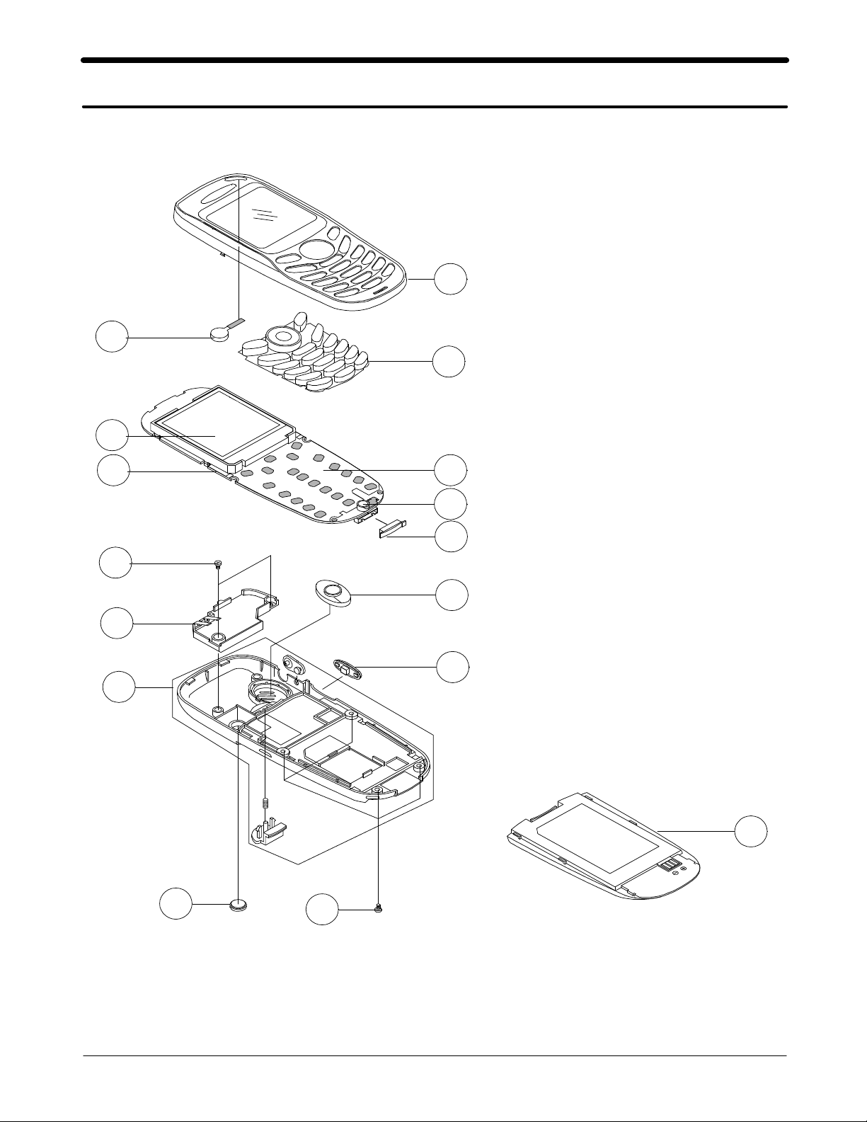
3. SGH-X100 Exploded View and its Parts list
1. Cellular phone Exploded View
1
3
2
9
10
11
12
13
4
5
6
7
8
16
14
15
3-1
SAMSUNG Proprietary-Contents may change without notice
This Document can not be used without Samsung's authorization
Page 10
SGH- X100 Exploded view and its Part list
2. Cellular phone Parts list
NO DESCRIPTION SEC CODE REMARK
1 FRONT COVER GH75-03497A
2 KEYPAD GH75-03518A
MOTOR GH31-00064A
3
4 DOME SHEET GH59-00929A
5 MIC GH30-00044A
6 IF COVER GH73-02203A
7 MICRO SPEAKER 3001-001445
8 VOLKEY GH75-03728A
9 LCD GH07-00394A
10 MAIN PBA GH92-01558A
11 SCREW 6001-001654
12 INTENNA GH42-00308A
13 REAR COVER GH75-03496A
14 RF COVER GH72-09251A
15 SCREW 6001-001654
16 BATTERY GH43-00994A
3-2
SAMSUNG Proprietary-Contents may change without notice
This Document can not be used without Samsung's authorization
Page 11
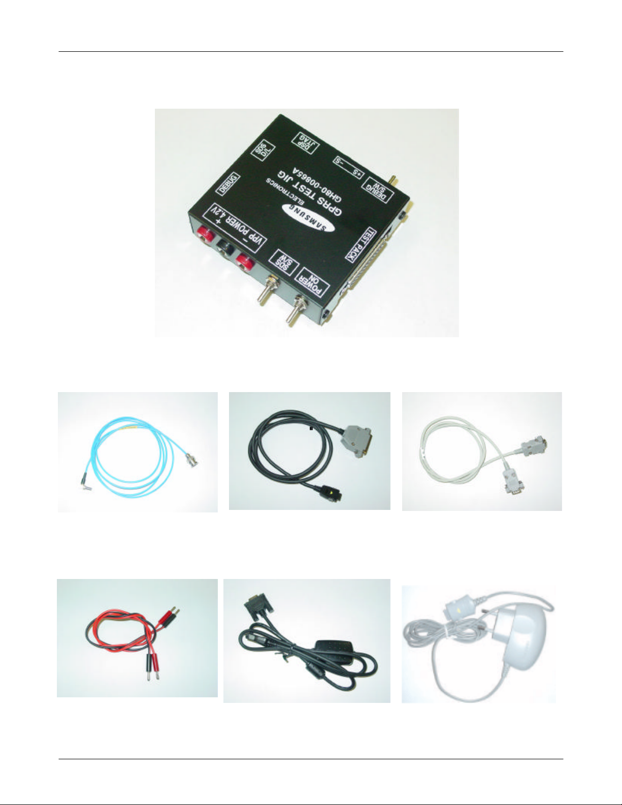
3. Test Jig (GH80-01909A)
SGH-X100 Exploded view and its Part list
3-1. RF Test Cable
(GH39-00140A)
3-2. Test Cable
(GH39-00217A)
3-4. Power Supply Cable 3-5. DATA CABLE
(GH39-00219A)
3-3. Serial Cable
3-6. TA
(GH44-00482G)
3-3
SAMSUNG Proprietary-Contents may change without notice
This Document can not be used without Samsung's authorization
Page 12
4. SGH-X100 MAIN Electrical Parts List
SEC CODE Design LOC
0403-001427 ZD601
0403-001446 ZD600
0404-001089 D600
0406-001104 Q400
0504-001012 Q400
0504-001012 Q401
0504-001042 U104
0504-001042 U106
0504-001134 Q301
0505-001332 Q302
0505-001423 U410
0506-000107 U405
0601-001402 RI401
SEC CODE Design LOC
1201-001954 U101
1202-001036 U203
1203-002633 U307
1203-002980 U309
1204-002161 U301
1205-002257 U400
1205-002276 U200
1205-002327 U103
1404-001221 TH200
2909-001204 U100
1405-001082 V202
1405-001082 V204
1405-001082 V205
0601-001611 LED402
0601-001611 LED405
0601-001611 LED408
0601-001611 LED409
0601-001647 LED401
0601-001647 LED403
0601-001647 LED404
0601-001647 LED406
0601-001647 LED407
0601-001647 LED410
0801-002237 U300
0801-002540 U210
0801-002540 U303
0801-002540 U304
1405-001082 V207
1405-001082 V211
1405-001082 V212
1405-001082 V400
1405-001082 V402
1405-001082 V403
1405-001082 V404
1405-001121 V405
1405-001121 V407
1405-001121 V506
2007-000137 R434
2007-000138 R132
2007-000140 R123
2007-000140 R124
1001-001183 U212
1003-001440 Q403
1109-001280 U305
SAMSUNG Proprietary-Contents may change without notice
This Document can not be used without Samsung's authorization
2007-000140 R305
2007-000140 R324
2007-000141 R105
4-1
Page 13
SGH-X100 Electrical Parts List
SEC CODE Design LOC
2007-000141 R225
2007-000141 R226
2007-000143 R135
2007-000143 R136
2007-000143 R137
2007-000143 R138
2007-000143 R362
2007-000144 R115
2007-000147 R116
2007-000148 R126
2007-000148 R202
2007-000148 R204
2007-000148 R205
SEC CODE Design LOC
2007-000162 R350
2007-000162 R360
2007-000162 R361
2007-000162 R436
2007-000171 R100
2007-000171 R107
2007-000171 R109
2007-000171 R139
2007-000171 R213
2007-000171 R214
2007-000171 R228
2007-000171 R307
2007-000172 R120
2007-000148 R210
2007-000148 R227
2007-000148 U732
2007-000157 R321
2007-000162 R102
2007-000162 R103
2007-000162 R203
2007-000162 R211
2007-000162 R212
2007-000162 R229
2007-000162 R234
2007-000162 R270
2007-000162 R300
2007-000162 R302
2007-000172 R131
2007-000174 R129
2007-000242 R200
2007-000242 R206
2007-000566 R125
2007-000566 R127
2007-000636 R432
2007-000636 R433
2007-001217 R425
2007-001288 R108
2007-001288 R112
2007-001301 R401
2007-001301 R404
2007-001301 R407
2007-000162 R303
2007-000162 R304
2007-000162 R306
SAMSUNG Proprietary-Contents may change without notice
This Document can not be used without Samsung's authorization
2007-001301 R408
2007-001305 R118
2007-001305 R122
4-2
Page 14

SGH-X100 Electrical Parts List
SEC CODE Design LOC
2007-001305 R230
2007-001305 R231
2007-001308 R110
2007-001308 R111
2007-001308 R113
2007-001308 R114
2007-001313 U735
2007-001325 U734
2007-001339 R430
2007-001339 R431
2007-003025 R328
2007-007001 R218
2007-007001 R219
SEC CODE Design LOC
2007-007573 R428
2007-007588 R429
2007-007981 R224
2007-008312 R221
2007-008354 R427
2203-000233 C119
2203-000233 C120
2203-000233 C144
2203-000254 C145
2203-000254 C209
2203-000254 C301
2203-000254 C408
2203-000254 U726
2007-007008 R426
2007-007009 R400
2007-007009 R402
2007-007009 R403
2007-007009 R405
2007-007009 R406
2007-007009 R409
2007-007100 R415
2007-007107 R201
2007-007107 R209
2007-007136 R311
2007-007137 R310
2007-007137 R313
2007-007148 R104
2203-000278 C102
2203-000278 C104
2203-000278 C136
2203-000278 C140
2203-000278 C223
2203-000278 C234
2203-000278 C404
2203-000330 C409
2203-000330 C413
2203-000359 C124
2203-000359 C314
2203-000386 C210
2203-000386 C211
2203-000386 C229
2007-007311 R128
2007-007334 R215
2007-007480 R220
SAMSUNG Proprietary-Contents may change without notice
This Document can not be used without Samsung's authorization
2203-000438 C142
2203-000438 C236
2203-000438 C237
4-3
Page 15

SGH-X100 Electrical Parts List
SEC CODE Design LOC
2203-000438 C304
2203-000438 C310
2203-000440 C127
2203-000550 C147
2203-000585 C137
2203-000609 C148
2203-000679 C224
2203-000679 C233
2203-000679 C307
2203-000679 C308
2203-000679 C450
2203-000679 U736
2203-000812 C118
SEC CODE Design LOC
2203-002443 C135
2203-003054 C220
2203-003054 C231
2203-005054 C201
2203-005054 C217
2203-005056 C222
2203-005057 C112
2203-005057 C115
2203-005057 C122
2203-005057 C134
2203-005057 C150
2203-005057 C156
2203-005061 C113
2203-000812 C213
2203-000812 C219
2203-000812 C230
2203-000854 C108
2203-000854 C110
2203-000854 C114
2203-000940 C139
2203-000995 C203
2203-000995 C215
2203-000995 C225
2203-000995 C226
2203-000995 C227
2203-000995 C228
2203-000995 C471
2203-005061 C116
2203-005061 C121
2203-005061 C133
2203-005061 C149
2203-005061 C155
2203-005061 C204
2203-005061 C205
2203-005061 C206
2203-005061 C207
2203-005061 C208
2203-005061 C212
2203-005061 C221
2203-005061 C242
2203-005061 C243
2203-001153 C146
2203-001652 C411
2203-001652 C423
SAMSUNG Proprietary-Contents may change without notice
This Document can not be used without Samsung's authorization
2203-005061 C244
2203-005061 C245
2203-005061 C246
4-4
Page 16

SGH-X100 Electrical Parts List
SEC CODE Design LOC
2203-005061 C247
2203-005061 C248
2203-005061 C249
2203-005061 C250
2203-005061 C251
2203-005061 C305
2203-005061 C311
2203-005061 C316
2203-005061 C400
2203-005061 C402
2203-005061 C403
2203-005065 C416
2203-005065 C421
SEC CODE Design LOC
2203-005503 C152
2203-005503 C153
2203-005503 C154
2203-005840 C350
2203-006053 C126
2203-006053 C412
2203-006053 C424
2203-006053 C426
2203-006053 C427
2203-006053 C428
2203-006053 C429
2203-006053 C476
2203-006090 C418
2203-005065 C425
2203-005138 C123
2203-005444 C303
2203-005481 C130
2203-005482 C235
2203-005482 C238
2203-005482 C306
2203-005482 C309
2203-005482 C313
2203-005482 C410
2203-005482 C420
2203-005482 C470
2203-005482 C472
2203-005496 C141
2203-006090 C419
2203-006105 C312
2203-006105 C401
2203-006105 C407
2203-006105 C415
2203-006105 C422
2203-006201 C414
2203-006201 C417
2301-001197 C125
2301-001213 C128
2404-001020 C132
2404-001086 C319
2404-001101 C318
2404-001225 C406
2203-005496 C315
2203-005503 C138
2203-005503 C151
SAMSUNG Proprietary-Contents may change without notice
This Document can not be used without Samsung's authorization
2404-001239 C129
2404-001239 C131
2503-001053 CA401
4-5
Page 17

SGH-X100 Electrical Parts List
SEC CODE Design LOC
2503-001053 CA402
2503-001053 CA403
2503-001053 CA404
2703-000172 L300
2703-001709 L114
2703-001751 L110
2703-001751 L115
2703-001751 L121
2703-001791 L106
2703-002198 L117
2703-002201 L109
2703-002201 L111
2703-002203 L108
SEC CODE Design LOC
3710-001853 BAT301
3711-004988 SPK201
3722-001715 EAR201
4302-001130 BAT401
2703-002208 L105
2703-002208 L107
2703-002268 L116
2703-002519 L119
2801-004025 X400
2806-001317 OSC100
2809-001279 OSC101
2901-001246 U302
2901-001254 L120
2904-001417 F101
2904-001424 F102
3301-001105 L400
3404-001152 SW1
3404-001152 SW2
3705-001322 CN100
3709-001244 CN400
3710-001611 CN301
SAMSUNG Proprietary-Contents may change without notice
This Document can not be used without Samsung's authorization
4-6
Page 18

5. SGH-X100 Block Diagrams
1. RF Solution Block Diagram
HITACHI METAL ANT S/W
SHS-M090TC
Imax = 10 mA
Freq (MHz) Loss
880 - 915 1.1 dB
925 - 960 0.8 dB
1710 -1785 1.3 dB
1805 -1880 1.15 dB
Atten 2xfo : 39dB,30dB(GSM,DCS)
3xfo : 35dB,20dB(GSM,DCS)
EPCOS EGSM RX SAW Filter
B7820 (2.0X1.4)
IL=1.9dB typ 2.7dB max
Ripple=0.8dB typ 1.4dB max
Pins IA,IB,QA and QB
VIQ : 1.25V
V
mod
: 0.5V
+
-
I OUT
I OUT
typ
pp
. , 1.15V
min
, 1.35V
max
EGSM_MODE_SW
DCS_MODE_SW
VCC_RX_TX
Vc_EGSM
Inverter circuits
Vc_DCS
Vcc_Tx_BURST
SAWTEK DCS RX SAW Filter
856079 (2.5X2)
IL=2.8dB typ 3.5dB max
Ripple=0.8dB typ 1.8dB max
Vcc_RF_LO
Vcc_RF_VCO
Discrete
3rd Order
Loop Filter
fc = ? kHz
OFFSET Mixer input power
-16dBm max, -22dBm min
~
~
GSM S/W
DCS S/W
GSM/DCS/PCS
FESW1
FESW2
CP
VREG
~
QUAD
DIV
CP
60/114MHz
PFD
Philips Transceiver
UAA3536
FracN
DIV
PFD
DIV
QUAD
f
TXIF
100 kHz+fmod
+
Q OUT
-
Q OUT
Vcc_SYN
VREG
Vcc_REF(2.4V typ.)
f
compRF
=26MHz
REFIN
VTCXO
26MHz
I+
1:1/
2
I-
Q+
fmod
3
W
BUS
CTL
REG
DATA
CLK
EN
Q-
PW
R
EN
RXON
TXON
SYNON
FESWON
GSM
VAPC
DCS/PCS
VBAT
Micro Devices Quadband PAM
RF3140 (10 X10)
GSM: Pout = 35.0 dBm Eff = 60%
DCS: Pout= 33.0 dBm Eff = 55%
?㉥???TX VCO
VOU1810F27KRA (8.0X6.0X1.6)
GSM =
880 ~ 915MHz
(Vt=0.5V ~ 3.0V )
kV = 55+-11 MHz/V Typ
DCS =
1710 ~ 1785MHz
(Vt=0.5V ~ 3.0V )
kV = 115+-23 MHz/V Typ
Pout= 6.5+-3 dBm typ.,Ic <= 30mA
Harmonics <= -10dBc
SAMSUNG Proprietary-Contents may change without notice
This Document can not be used without Samsung's authorization
VCC_SYN
VCC_RX_TX
VCC_RF_VCO
VCC_TX_BURST
VCC_CP
(4.0V , 25mA )
5-1
(2.7V , 100mA )
(2.7V ,100mA )
(2.70V , 100mA )
(2.7V , 100mA )
RF1_VDD
RF2_VDD
RF1_VDDS
RF2_VDDS
HVS
VBat
(3.6V typ 3.0V min)
PMU
VDD1
(1.35V min 2.95V max , 150mA )
VDD2
(1.35V min 3.45V max , 150mA )
VDD3
VDD4
(1.35V min 3.45V max , 100mA )
(1.35V min 3.45V max , 150mA )
PON_TX
PON_SYNT
V_MODE
AVDD
(1.35V min 2.65V max , 100mA )
Page 19

SGH-X100 Block Diagrams
2. Base Band Solution Block Diagram
5-2
SAMSUNG Proprietary-Contents may change without notice
This Document can not be used without Samsung's authorization
Page 20

6. SGH-X100 PCB Diagrams
1. Main PCB Top Diagram
6-1
SAMSUNG Proprietary-Contents may change without notice
This Document can not be used without Samsung's authorization
Page 21

SGH-X100 PCB Diagrams
2. Main PCB Bottom Diagram
6-2
SAMSUNG Proprietary-Contents may change without notice
This Document can not be used without Samsung's authorization
Page 22

7. SGH-X100 Flow Chart of Troubleshooting
1. Power On
' Power On ' does not work
Check the Battery Voltage
is more than 3.4V?
Yes
C411(V_ISUP) = 2.7V Check the PMU related to V_ISUP
Yes
Check the Clock at
C410=32KHZ
Yes
C429 (VDD1) = "H" Replace the PBA
Yes
C428(VDD2), C427(VDD3) =
2.8V
No
Change the Battery
No
No
Resolder X400
No
No
Replace PBA
Yes
Check for the clock at C145
= 13MHz
Yes
Check the initial operation
END
SAMSUNG Proprietary-Contents may change without notice
This Document can not be used without Samsung's authorization
No
7-1
Check the clock generation circuit
(related to OSC101)
Page 23

SGH-X100 Flow Chart of Troubleshooting
Power On
VCC_TX_BURST
VCC_RF_VCO
VCC_RX_TX
VCC_SYN
PON_SYN
T
E6
RF1SW
S
LINREG)
C417
1U
F
H8
PUMP+
HVSVD
D
D9
C416
RF2SN
S
(CHARGE
HVSO
C
D8
4.7UF
F8
G9
RF2VD
RF1SN
D
S
LINREG
SUPPLY
HVSSCN
HVSSCP
B9
C9
C415
G8
F9
RFVBAT
RF1VD
D
HIGH VOLTAGE
HVSVBAT
HVSGN
D
C8
A9
PON_TX
10U
C418
F
C419 10U
F
100N
C420
F
VDD3
VDD2
AVD
D
V_MODE
TP403
VDD_AM
AVDD_TEM
P
P
VDD1
VBAT
V_ISU
P
VDD_VI
B
KEY_O
N
VDD_KEY
C426
1U
F
C427
1UF
C428
1U
F
C429
1UF
470N
C423
F
6.3V C422 10U
F
C424
1UF
G6
VPRO G
C3
H4
VSS1
E8
VSS2
C5
VSS3
VSS4
A8
VSS5
J1
VSS6
F1
F2
E7
G2
DVDD2VBA T
G1
E5
H2
H1
F7
B4
A4
H7
J7
G7
B5
A5
B3
A3
DVDD1
DVDD1VBA T
SEL12RB
DVDD2
SEL3RB
DVDD3VBA T
DVDD3
DVDD4ON
DVDD4VBA T
DVDD4
AVDD1VBA T
AVDD
AVDDS
HFAVBA T
HFAVDD
VIBVBA T
VIBVD D
NC1
D4
1UF
100N
C470
F
H9
E9
F6
RF2VDDS
RF1VDDS
RF2SW
S
SWITCH
DVDD1
DVDD2
DVDD3
DVDD4
AVDD
HFA
VI B
NC2
C4
C421
2.2U
F
BLM11A102SPT
L400
VCC_CP
2.2U
C414
F
B7
BBMGN
D
CONTRO
L
A7
B6
A6
BBMSW
BLVBAT
BLVD
D
BACKLIGHT
SUPPLY &
CONTRO
CHARG
E
L
CHRVBAT
CHRREG
CHRI
V
E3 E2
E1
VBAT
VBAT
F
G5
ISUPD
internal
suppl
y
VBAT
MONITO
VOLTAG
E
R
10M
1
12PF
C413
C412 1U
470N
C411
F
H5
ISUPA
MODUL
SUPPLY
E
REAL-TIME
CLOCK
BATTERY
R415
32K
VDD_3V05
V_ISUP
C410
100N F
J3
J4
VBAT
VSAVE
INTERNAL
SENSO
R
PLL
OSCILLATOR
32KHz XTAL
OSCO
OSCI
J8
J9
2
TEMP HIGH
htmp
clocks
GENERATOR
FC-255
X400
12PF
C409
internal
CLOCK
J5
MICBIAS
calibration
4.7U
C405
F
10UF
C406
10PF C404
C408
10NF
4.7U
C407
F
BAT401
RB414_IV02N
VBAT
REFGN
refgnd
D
REFERENCE
MIC BIAS
&
voltag
bias current
referenc
e
e
s
ovdd
htmp
SIMCLK
CPRES
SIMI
O
C6
C7
D3
TP401
TP402
SIMI
SIMCLK
O
MIC_BIAS
J6
H6
REFC
ON-CHIP
statu
data
s
GENERATO R
INTERFACE
SI
M
SD
SCL
A
E4
F3
SCL
SD
A
INTERFACE
12C
contro
l
CONTRO
ON/OF
F
L
INTERRUPT
CLK
RST
IO
C1
D1
D2
SIM_IO
SIM_RST
SIM_CL
K
CHARG
PUMP
E
VCC
C2
SIM_VCC
U400
PCF50601ET-N5
SLPMOODN
AUXONN
ONKEY_N
RSTO N
CLK32
REC2
REC1
REC3
SIMVBA T
SI
SIMGND
M
SIMSCP
SIMSCN
INTN
100N
F
C403
TM
CHARGER_O
REF_O
K
N
PMU (IC
)
F5
D5
G4
F4
D6
B8
H3
J2
G3
D7
B2
A2
B1
A1
100N
F
ONKEY_N
RSTO
N
C400
JACK_I
JIG_REC
IT_PM
RECO
32K
N
U
1
R410
10K
VDD1
U732
10K
VDD1
VBAT
7-2
SAMSUNG Proprietary-Contents may change without notice
This Document can not be used without Samsung's authorization
Page 24

2. Initial
SGH-X100 Flow Chart of Troubleshooting
Initial Failure
Yes
The node between R202 and
C209 ="H" (RSTON)
Yes
U303 pin 4,6 (memory
CE) is OK?
Yes
Check the circuit around
LCD & U303
END
No
Check the circuit related to reset
No
Replace PBA
7-3
SAMSUNG Proprietary-Contents may change without notice
This Document can not be used without Samsung's authorization
Page 25

SGH-X100 Flow Chart of Troubleshooting
AVDD_TEM
P
Initial
CTS0
RTS0
TXD0
RXD0
RXD1
TXD1
TD I
TM S
TC K
TD O
TRST_N
J_SEL
R234
100K
TD I
TM S
TC K
TD O
TRST
U733
VDD3
TP504
B5
A5
C5
C4
N1 0
N1 4
N1 1
G1 3
E13
D1 1
A1 2
C1 1
RI_RED RI_BLUE
IT_PM
U
KBIO(0:7)
KBIO(0) KBIO(1) KBIO(2) KBIO(4) KBIO(5) KBIO(6) KBIO(7)
K11
J1
0
KBIO2
KBIO0 KBIO1
CTS0_N
RXT0_N
TXD0
RXD 0
D4
RXD 1
A4
TX D
D2
TD I
A2
TM S
A3
TC K
D3
TD O
A1
TRST_N
B4
J_SEL
P10
AVSS
K7
VSS_A
J1
VSS_B
M7
VSS_C
VSS_E
VSS_F
VSS_G
VSS_H
E8
VSS_I
C3
VSS_K
G1
VSS_M
K1
VSS_N
P1
VSS_O
N5
VSS_P
VSS_BB
VSS_D
C1 3
VSS_REF
VSS_VB
VSS_VBOUT
SIMCLK SIMI
SCL SD
A
O
KBIO(3)
K13
J1
1
KBIO3
KBIO4
KBS
JTAG
PWM0
F4
L11
L13
L12
L14
KBIO5
KBIO6
KBIO7
UART0
UART1
PWM
SIMCLK
SIMERR
PWM1
SIMI
O
M1
M1
M1
E6
4
1
3
R225
2.2K
2.2K
R226
END_OF_CHARG
KEY_O
CTS0
N
E
N8
K8
P6
GPIO1
GPIO8 GPIO9
0
SIMU
IIC
SD
SCK
A
C2
B3
VDD2
AUDIO_SW
KEY_LOCK
LCD_SEL
2
N7
L7
L9
GPIO5
GPIO6
GPIO7
GPI
O
SC
BIOCLK
BDIO
BIEN
E11
F10
F11
BIOCLK
BACKLIGHT
LED_SYN
CHG_ON
C
M9
P7
L8
GPIO2
GPIO3
GPIO4
BOEN
ACLK
AD
O
G11
B8
A9 B9
TP208
TP209
BOEN BIEN BDIO
DU DC
L
AUDIO_SW
M_RST
1
M1
K9
2
GPIO0
GPIO1
AFS
AD
I
A8
TP210
TP207
FSC DD
SUB_MEL_CS_I
NCSFLASH
NCSRAM
N
M5
N4
G5
CS_N1
CS_N2
CS_N0
PCF50732
D
AUXMIC
MCLK
N
D1
A14
0
AUX_MIC_N AUX_MIC_P MIC_N MIC_P
3.9K
D_REF_13M
LCD_CS
G3
CS_N3
A
AUXMIC
P
B14
R218
HWR_N
HRD_
N
H5
HRD_
HWR_N
N
ASI
MICN
MICP
A13
B13
100K
R212
100K R270
HWR_N
100K
R211
HA(23) HA(22) HA(21)
HA(20) HA(19) HA(18) HA(17) HA(16)
G4
N6
P5
L5
L6
HA22
HA23
HA20 HA21
SIOY
D
A
AUXSP
EARN
EARP
BU
Z
A11
B10
B11
A10
REC_P REC_N AUXSP
LINE_OUT
VDD1
100K,1%
R201
TH200
B57231-V2473-J60
HA19
K2
K4
HA18
AUXADC4
F13
R205
10K
VF
VDD3
VDD3
VDD2
HA(15) HA(14) HA(13) HA(12) HA(11) HA(10) HA(9
K3
J5
J4
J2
HA15
HA16
HA17
D
AUXADC1
AUXADC2
AUXADC3
J1
F14
G14
E14
4
IRX_TX_N IRX_TX_P QRX_TX_N
MES_BATT
M2
HA12
HA13 HA14
SIOX
A
IN
IP
J1
3
10K
100K,1%
R209
L2
L1
HA11
BSI
A
D
QN
QP
H14
H13
QRX_TX_P
R210
HA10
A
N1
)
M1
HA
9
D
AUXDAC3
D1
2
RAM
P
HA(8
HA(7
)
)
N2
P2
HA
HA
HA
6
7
8
EMI
DSP
D
A
AUXDAC1
AUXDAC2
E12
D1
3
AFC
AVDD_TEM
P
HA(1:23)
HA(6
HA(5
HA(4
HA(3
HA(2
HA(1
)
)
)
)
)
)
HD(15) HD(14) HD(13) HD(12) HD(11) HD(10) HD(9) HD(8) HD(7) HD(6) HD(5) HD(4) HD(3) HD(2) HD(1) HD(0)
M3
M4
N3
K5
HA
HA
HA
3
4
5
D1
B2
L4
P3
E3
E2
HD1
HD1
HD1
HD1
HA
HA
2
1
4
5
2
3
CSI
D
D
D
A
A
A
RFE_N
RFE_N
VRE
F
2
C14
K12
C221
100N
F
RF_EN_SYN
T
CEN
0
J1
D9
2
F2
E4
F3
F1
E1
HD8
HD9
HD7
HD1
HD1
0
1
RFCU
RXO
TXO
CCLK
CD
CD
O
N
N
I
G12
H12
D8
E9
E10
RF_BBI_DATA RF_BBI_CLK
H1
B1
HD5
HD6
RFSIG10
RFSIG9
K10
D7
PON_RX
PON_TX
E5
J3
HD3
HD4
RFSIG7
RFSIG8
C6
E7
ANT_SW
PON_SYN
3
T
H2
HD2
HD1
RFSIG5
RFSIG6
B7
ANT_SW
2
RSTO
N
100K
M1
H1
C10
0
0
RSTO_N
RST_N
RESETN
OOL
PCF50874
PDCU
RFSIG0
RFSIG1
D5
A6
TXVCO_SW
TXVCO_SW
1
2
10N
C209
F
R203
P13
P14
CKI32I
CKI32O
CGU
VDDC_ A
VDDC_ B
VDDC_ C
VDDC_ D
VDDE1_A
VDDE1_B
VDDE1_C
VDDE1_D
VDDE2_C
VDDE2_E
VDDE3_A
VDDE3_B
VDDE3_F
VDDE3_G
VDD_REF
VDD_VB
VDD_VBOUT
GPON1
AUXST
L10
G10
TP211
REF_O
V_MODE
N
R202
10K
P11
CKI
AVDD
VDD_BB
VDD_ D
GPON2
N9
TP200
D_REF_13M
32K
OM6357
F5
N1 3
M8
K6
P9
N1 2
C8
H1 1
P8
C1
P4
M6
G2
L3
P12
F12
C9
D1 4
B12
C1 2
U200
NC C218
VDD1
VDD1
VDD2
VDD3
AVD
D
VDD1
AVD
D
HD(0:15)
H4
H3
K14
HD0
AUXO
N
RFSIG2
RFSIG3 RFSIG4
D6
B6
A7 C7
TP202
TXVCO_SW
ANT_SW
1
3
7-4
SAMSUNG Proprietary-Contents may change without notice
This Document can not be used without Samsung's authorization
Page 26

3. Charging Part
SGH-X100 Flow Chart of Troubleshooting
Abnormal charging part
Check the U309 pin 4 > 4.9
V ?
Yes
U309 pin 5 = "H"
Yes
Q301 pin 1 (CHG_ON) = "L"
Yes
Check the U309 pin 3 =
4.2V
Yes
END
No
No
No
No
Check the circuit related to
V_EXT_CHARGE
Resolder or replace U309
Check the circuit related to
CHG_ON signal
Resolder or replace U309
7-5
SAMSUNG Proprietary-Contents may change without notice
This Document can not be used without Samsung's authorization
Page 27

SGH-X100 Flow Chart of Troubleshooting
Charging
7-6
SAMSUNG Proprietary-Contents may change without notice
This Document can not be used without Samsung's authorization
Page 28

4. Sim Part
Phone can't access SIM Card
Yes
CN400 pin 1,5 = "H"
Yes
SGH-X100 Flow Chart of Troubleshooting
No
Replace PBA
Check SIMCLK Signal on CN400
After Power ON,
pin3 in a few second
Yes
After SIM card insert,
CN400 pin 2 = "H(SIMRST)"
Yes
Check the SIM Card
END
No
Replace PBA
No
Replace PBA
7-7
SAMSUNG Proprietary-Contents may change without notice
This Document can not be used without Samsung's authorization
Page 29

SGH-X100 Flow Chart of Troubleshooting
5. Microphone Part
Microphone does not work
Yes
Check the connection
from MIC
Yes
Check the circuit
from U200 to MIC
No
Resolder MIC
No
Resolder the C200, C201, C203, C208,
C210, C211, C212, C213, C215, C216, C217
R200, R204, and R206
Yes
Check the MIC
Yes
END
No
Replace the MIC
7-8
SAMSUNG Proprietary-Contents may change without notice
This Document can not be used without Samsung's authorization
Page 30

SIM
A2
A1B1
B2
T
SIMSCP
SIMGND
SIMVBA
SIM
CHARGE
PUMP
SIM
INTERFACE
SIMSCN
VCC
CLK
RST
IO
CPRES
SIMIO
SIMCLK
C2
D2
C1
D1
D3
C7
C6
SIM_VCC
SIM_CLK
SIM_RST
SIM_IO
TP401
TP402
V400
SIMIO
SIMCLK
C401
4.7UF
100NF
V401
C402
SGH-X100 Flow Chart of Troubleshooting
CN400
PC-D6-A6-H2.9-S
66
55
G
7GG89
V402
NC
C450
V403
11
22
33 44
G
10
NC
C451
C452
NC
Microphone
V214
MIC201
MIC_PAD
V215
C200
33PF
C210
15PF
C216
33PF
C201
10PF
C213
9PF
C217
10PF
MIC_BIAS
R200
1.5K
X400
L201
27nH
L202
27nH
C409
R206
1.5K
C208
100N F
C212
100N F
R204
10K
C203
39PF
C211
56PF
C215
39PF
MIC_P
MIC_N
7-9
SAMSUNG Proprietary-Contents may change without notice
This Document can not be used without Samsung's authorization
Page 31

SGH-X100 Flow Chart of Troubleshooting
6. Speaker Part(Melody)
Speaker does not work
U300 pin 5 = 2.85V
No
Resolder or replace U300
Yes
Check the Clock signal at
Pin 1 of U301 (13MHz)
is OK?
Yes
U301 pin 17, 18≒ 1.8V
Yes
Is Speaker working?
END
No
Check the clock generation circuit
(related to OSC101 and U300)
No
Resolder U301
No
Check the Spearke Contact and
change the Speaker
7-10
SAMSUNG Proprietary-Contents may change without notice
This Document can not be used without Samsung's authorization
Page 32

Speaker
LINE_OUT
220NF
1.2K,1%
SUB_MEL_CS
3
_E
GND
VCC
Y1
4
C315
R313
R310
1.2K,1%
R311
4.7K,1%
150PF
C314
LCD_SEL
1
25
A
Y0
6
MELODY_CS
100K
NC7SZ19P6X
U304
VDD3
C311
68NF
R307
0
VDD3
R350
1NF
1uF
100NF
100NF C306
10
11
12
13
14
15
16
C310
C350
C309
9
VSS
VREF
HPOUT-L/MONO
HPOUT- R
EQ1
EQ2
EQ3
SPVDD
SPVSS
SPOUT2
SPOUT1
17
3.3K
18
8
R306
VDD
MT
R
19
10NF
7
PLLC
20
M_RST
C301
4
5
6
/RST
NC
/IRQ
YMU762 MA-3
U301
D6
D7
D4
D5
22 21
SGH-X100 Flow Chart of Troubleshooting
MELODY_CL
K
2
1
NC
VCC
5
32
31
30
29
28
27
26
TC7SH04FU-TE85L
U300
VDD2
VDD3
VDD3
C300
NC
LED_SYNC
3
2
LED
D3
24 23
3
GND
OUT
4
CLKI
IOVDD
D2
25
330
1
/R D
A0
/C S
/W R
D0
D1
IN
R304
C303
AMP_P
3PF
27PF
C304
AMP_N
HD(7)
HD(6)
HD(5)
HD(4)
HD(3)
HD(2)
HD(0)
HD(1)
HA(23
MELODY_CS
HWR_N
)
HRD_N
6.3V 4.7UF
100NF C313
C312
VBAT
C307
27PF
27PF C308
7-11
SAMSUNG Proprietary-Contents may change without notice
This Document can not be used without Samsung's authorization
Page 33

SGH-X100 Flow Chart of Troubleshooting
7. Key Data Input
Check Initial Operation
Yes
When one or the keys is
When one of the keys is
pushed,
is it displayed on LCD
Yes
pushed,
KBIO signal is OK?
Yes
END
No
Check the Dome sheet & Key Pad
No
Replace the PBA
7-12
SAMSUNG Proprietary-Contents may change without notice
This Document can not be used without Samsung's authorization
Page 34

8. Receiver Part
Receiver does not work
EAR201 pin 2,3 = short
EAR201 pin 2,3,6 = 1.5V
SGH-X100 Flow Chart of Troubleshooting
Yes
No
Resolder EAR201
Yes
No
Replace the PBA
Yes
Is Receiver working?
Yes
END
No
Check the Receiver contact and
Replace the Receiver
7-13
SAMSUNG Proprietary-Contents may change without notice
This Document can not be used without Samsung's authorization
Page 35

SGH-X100 Flow Chart of Troubleshooting
9. Back Light (for Color Main LCD)
Backlight does not work
Yes
LCD Contrast high level
in the Menu?
Yes
U307 pin 5 > 3.35
No
Select LCD Contrast high level
No
Resolder U307
Yes
U307 pin 4 = "H"
Yes
U307 pin 1 ≒ 10V
Yes
Backlight does work?
Yes
No
No
No
Replace the PBA
Check U307 and L300
Check D600, ZD600 and resolder LCD
Or replace the LCD Module
Module.
END
7-14
SAMSUNG Proprietary-Contents may change without notice
This Document can not be used without Samsung's authorization
Page 36

10. Key Back Light
Key Backlight does not work
Between C426 and R400 =
"H"
END
SGH-X100 Flow Chart of Troubleshooting
Yes
No
Check the PMU related to "VDD_KEY"
Yes
7-15
SAMSUNG Proprietary-Contents may change without notice
This Document can not be used without Samsung's authorization
Page 37

SGH-X100 Flow Chart of Troubleshooting
11. GSM Receiver
RF input : CH center freq : +67.7kHz
RX ON
Amp : -50dBm
Yes
U100 Pin5
>= -65dBm
Yes
U100 pin7
>= -65dBm
Yes
F101 pin1
>= -70dBm
Yes
U103
pin32 >= -70dBm
pin33 >= -70dBm
No
No
No
No
Resolder CN100, C108
Check U100
pin8 = L, pin4 = L
Yes
Resolder F101, C110, L108
Resolder L105, L106, L107
No
Check ANT Switch
control circuit
Resoder U100
Yes
U103 pin6, 7, 8, 9
>= 1V
Yes
R135, R136, R137,
R138 >= 1V
Yes
Check U200
END
SAMSUNG Proprietary-Contents may change without notice
This Document can not be used without Samsung's authorization
No
Check U103
pin4, 10, 22 >=2.7V
Yes
7-16
No
?
Resolder U103
Page 38

12. GSM Transmitter
TX ON (5Level)
Yes
SGH-X100 Flow Chart of Troubleshooting
U100 Pin5
>= 20dBm
No
U100 pin1
>= 20dBm
No
F101 pin9
>= 20dBm
No
U101 pin7
>= -11dBm
No
U103 pin6, 7, 8, 9
>= 1V
Yes
Yes
Yes
Yes
Yes
Resolder CN100, C108
Check U100
pin8 = H (2.68V),
pin4 = L
No
Resolder L118, L119, L121
Check U101
+VBATT, pin4, 7
OK?
No
Resolder R112, R113, R114
Yes
Change or Resolder U100
Check ANT Switch
control circuit
Yes
Resolder or Change U101
Check +VBATT or PAM
control signal
No
R135, R136, R137,
R138 >= 1V
No
Check U200
END
SAMSUNG Proprietary-Contents may change without notice
This Document can not be used without Samsung's authorization
Yes
Check U103
pin4, 22 >= 2.7V
OK?
7-17
Yes
Resolder U103
Page 39

SGH-X100 Flow Chart of Troubleshooting
13. DCS Receiver
RF input : CH center freq : +67.7kHz
RX ON
Amp : -50dBm
Yes
U100 Pin5
>= -65dBm
Yes
U100 pin7
>= -65dBm
Yes
F102 pin1
>= -70dBm
Yes
U103
pin38 >= -70dBm
pin39 >= -70dBm
No
No
No
No
Resolder CN100, C108
Check U100
pin8 = L, pin4 = L
Yes
Resolder F102, C114, L116
Resolder L110, L114, L115
No
Check ANT Switch
control circuit
Resoder U100
Yes
U103 pin6, 7, 8, 9
>= 1V
Yes
R135, R136, R137,
R138 >= 1V
Yes
Check U200
END
SAMSUNG Proprietary-Contents may change without notice
This Document can not be used without Samsung's authorization
No
Check U103
pin4, 10, 22 >=2.7V
Yes
7-18
No
Check & Reslder
U103, R105, R109
RF13MHz, RF PSU Part
Resolder U103
Page 40

14. DCS Transmitter
TX ON (5Level)
Yes
SGH-X100 Flow Chart of Troubleshooting
U100 Pin5
>= 13dBm
No
U100 pin1
>= 13dBm
No
U101 pin11
>= 13dBm
No
U101 pin1
>= 15dBm
No
U108 pin5
>= 12dBm
Yes
Yes
Yes
Yes
Yes
Resolder CN100, C108
Check U100
pin8 = L,
pin4 = H (2.68V)
No
Resolder C118
Check U101
+VBATT, pin4, 7
OK?
No
Resolder R108, R110, R111
Yes
Change or Resolder U100
Check ANT Switch
control circuit
Yes
Resolder or Change U101
Check +VBATT or PAM
control signal
No
U101 pin5, 6, 7, 8
>= 500mV
No
Check U200
END
SAMSUNG Proprietary-Contents may change without notice
This Document can not be used without Samsung's authorization
Yes
Check U103
pin4, 22 >= 2.7V
OK?
7-19
Yes
Resolder U103
Page 41

SGH-X100 Flow Chart of Troubleshooting
Transmitter
NC U729
R109
0
R129 47
C136 10PF
10PF C140
46
42 43
44
45
40
GND2
GND3 GND4
NC1 NC2
FESWON
1
TXRFI
2
EXTRES
3
TXCP O
45
TXCPVC C
TXON
6
IA
7
IB
8
QA
9
QB
10
IFVC C
41
CAFCSUP
CLKFDBX
CLKOUT
GND1
11
12
13
1NF C142
220NF C141
3
OSC101
TCO-9141
OUT
GND
VCC
2
4
CTRL
1
100PF C144
10K R126
220K
R125
R127
220K
C143 NC
AFC
180PF C151
180PF C153
20PF C147
R131
10
VCC_CP
R139
0
C155 100NF
C156 8.2PF
100NF C149
C150
8.2PF
C152 180PF
C154 180PF
R136
R138
R135
R137
4.7K
4.7K
4.7K
4.7K
QRX_TX_P IRX_TX_N IRX_TX_P
QRX_TX_N
VCC_SYN
PON_TX
68PF C146
100
R132
22NF C148
NC
R134
D_REF_13M
10NF C145
MELODY_CLK
R128
22K,1%
120
120
R123
1K
39
DCSIB
330PF
220PF
C137
180PF
C138
TXVCO_SW1
38
DCSIA
REFGND
REFIN
14
470PF
C139
10
R121
0
RF_BBI_DATA
RAMP
C135
R118
R122
TXVCO_SW2
R124
1K
37
RFGND2
UAA3536HN
REFVCC
15
R120
R119
0
RF_BBI_CLK
8.2K
36
PCSIB
U103
16
R117
0
RF_EN_SYNT
C100
NC
DCS_PCS_TX
EGSM_TX
PCS_R
X
100UF
C131
VBAT
ANT_SW1 ANT_SW3
NFM18PC104R1C3D
L120
ANT_SW3
3 4
2
TXEN
BAND
VC C
GSM850/900IN
VCC2
VCC2
DCSIN
7
1
R110
200
18
R111 200
11
OSC100
7
30
29
28
27
26
25
24
23
22
21
TC7SH32FU(TE85L)
U107
2
1
A
B
GN
VCC
3
D
Y 4
10
8
12
RF3140
U101
R108
C128 6.8NF
VCC_RX_TX
5
0
R106
R13
0
3
TXVCO_SW3
NC R107
VCC_TX_BURST
C127
1NF
C126
1UF
1.8NF C123
390PF C125
R105 2.2K
3.6K R104
150PF C124
100PF C119
C120 100PF
8.2PF
C122
100NF C121
VCC_SYN
C118
33PF
3.9nH
L121
PON_RX PON_SYNT
100UF
C129
6.3V
C132 10UF
C471
47PF
13
R115 5.1K
VDD2
R116
10nH
L117
47NF
C130
6 5
VBATT
VRAMP
VREG
GSM850/900OUT
13
GND
PCSOUT
9
11
L119
NC
L118
NC
R113
200
R112
18
200 R114
5
1
8
CONTROL
OUT1
OUT2
10
NC
GND
12
VCC2
GND
9
VCC1
GND
6
GND
3
BAND
BAND
4
2
33
35
34
32
31
RFVCC
PCSIA
RFGND1
GSMIA
GSMIB
FESW 2
FESW 1
RFLOVC C
GNDTUNE
RFTUNE
RFVCOVCC
SYNON
RXON
SYNVC C
RFCPO
RFCPVCC
DATA
CLK
EN
20
17
19
18
100NF C133
8.2PF C134
VCC_CP
L109
L112
L111
33nH
33nH
33nH
10
4
8
SHS-M090T
VC1
VC2 VC3
2
GG
61
2
13
14
8.2nH L116
25
8.2PF C115
100NF C116
VCC_RF_VCO
U100
5
AN
G
T
DCS/PCS-TX
G
GSM-TX
GSM-RX
DCS-RX
PCS-RX
G
7
1 9
11
3
39PF C114
C110 39PF
NC L104
L108 15nH
1
856079
IN
F102
G
G
OUT
OUT
3 4
NC L113
3.9nH L115
L110 3.9nH
12nH L114
8.2PF
C112
100NF
C113
VCC_RX_TX
1
IN
B7820
25
G
G
OUT
OUT
3 4
C111 NC
L107 2.2nH
L106 15nH
F101
G
25
G
OUT
2.2nH L105
NC L103
NC L102
ANT_SW3 ANT_SW2 ANT_SW1
C101
NC
39PF C108
NC C109
1
IN
LE72E
F100
OUT
3 4
L101
NC
NC L100
DCS_PCS_TX
10PF C102
R103 100K
C105
NC
3
5
2
6
PCS_RX
C103 10PF
R101
100K
3
5
2
6
EGSM_TX
10PF C104
R102 100K
3
NC C107
5
2
6
ANT100
R100
0
1
G
2
A
3
CN10
C
KMS-158
4
0
G
5
G
6
G
BCR10P
U104
N
4
1
BCR10P
U105
N
4
1
BCR10P
U106
N
4
1
VCC_RX_TX
7-20
SAMSUNG Proprietary-Contents may change without notice
This Document can not be used without Samsung's authorization
 Loading...