

Page 1

LCD-TV
Chassis : N74A
Model : UA40B7000WM
UA46B7000WM
UA55B7000WM
Manual
SERVICE
TFT-LCD TV Contents
1. Precautions
2. Product specications
Disassembly and Reassembly
3.
Troubleshooting
4.
Exploded View & Part List
5.
Wiring Diagram
6.
UA40B7000WM/UA46B7000WM/
UA55B7000WM
Refer to the service manual in the GSPN (see the rear cover) for the more information.
Page 2

Contents
1. Precautions ..............................................................................................................1-1
1-1. Safety Precautions .........................................................................................................1-1
1-2. Servicing Precautions .....................................................................................................1-2
1-3. Electrostatically Sensitive Devices (ESD) Precautions ..................................................1-2
1-4. Installation Precautions ..................................................................................................1-3
2. Product specications ............................................................................................2-1
2-1. Feature & Specications .................................................................................................2-1
2-2. MJC : Motion Judder Cancellation (FRC) .......................................................................2-6
2-3. Internet@TV ...................................................................................................................2-7
2-4. Using the Content Library .............................................................................................2-16
2-5. Using the TV Memory Contents ....................................................................................2-17
2-6. Using the Content Management ...................................................................................2-18
2-7. Media Play ....................................................................................
2-8. Spec Comparison to the Old Models ............................................................................2-21
2-9. Accessories ...................................................................................
3. Disassembly and Reassembly ............................................................................... 3-1
3-1. Disassembly and Reassembly .......................................................................................3-1
4. Troubleshooting ......................................................................................................4-1
................................2-19
...............................2-22
4-1. Troubleshooting ..............................................................................................................4-1
4-2. Alignments and Adjustments ........................................................................................4-26
4-3. Factory Mode Adjustments ...........................................................................................4-27
4-4. White Balance - Calibration ..........................................................................................4-37
4-5. Servicing Information ....................................................................................................4-39
5. Exploded View & Part List ...................................................................................... 5-1
5-1. UA40B7000WM Exploded View .....................................................................................5-1
5-2. UA46B7000WM Exploded View .....................................................................................5-3
5-3. UA55B7000WM Exploded View .....................................................................................5-5
5-4. UA40B7000WM Parts List ..............................................................................................5-7
5-4. UA46B7000WM Parts List ............................................................................................5-38
5-5. UA55B7000WM Parts List ............................................................................................5-69
6. Wiring Diagram ........................................................................................................ 6-1
6-1. Wiring Diagram 40” .........................................................................................................6-1
6-2. Wiring Diagram 46/55” ....................................................................................................6-2
6-3. Connector Functions ......................................................................................................6-5
6-4. Cables ............................................................................................................................6-5
Page 3
GSPN (Global Service Partner Network)
Area Web Site
North America http://service.samsungportal.com
America http://latin.samsungportal.com
Latin
CIS http://cis.samsungportal.com
Europe http://europe.samsungportal.com
China http://china.samsungportal.com
Asia http://asia.samsungportal.com
Mideast
This
Any unauthorized use of Manual can be punished under applicable
International and/or domestic law.
& Africa http://mea.samsungportal.com
Service Manual is a property of Samsung Electronics Co.,Ltd.
© 2008 Samsung Electronics Co.,Ltd.
All rights reserved.
Printed in Korea
P/N: BN82-00636A-00
Page 4
1. Precautions
1. Precautions
1-1. Safety Precautions
Follow these safety, servicing, and ESD precautions to prevent damage and to protect against potential hazards such as
electrical shock.
1-1-1. Warnings
For continued safety, do not attempt to modify any circuitry.
1.
1-1-2. Servicing the LCD TV
When servicing the LCD TV, Disconnect the AC line cord from the AC outlet.
1.
It is essential that service technicians have an accurate voltage meter available at all times.
2.
Check the calibration of this meter periodically.
1-1-3. Fire and Shock Hazard
Before returning the LCD TV to the user, perform the following safety checks:
Inspect each lead dress to make certain that the leads are not pinched or that hardware is not lodged between the
1.
chassis and other metal parts in the LCD TV.
Inspect all protective devices such as nonmetallic control knobs, insulating materials, cabinet backs, adjustment and
2.
compartment covers or shields, isolation resistor capacitor networks, mechanical insulators, etc.
Leakage Current Hot Check (Figure 1-1):
3.
WARNING : Do not use an isolation transformer during this test.
Use a leakage current tester or a metering system that complies with American National Standards Institute (ANSI
C101.1, Leakage Current for Appliances), and Underwriters Laboratories (UL Publication UL1410, 59.7).
With the unit completely reassembled, plug the AC line cord directly into a 120V AC outlet. With the unit’s AC switch
4.
(READING SHOULD)
NOT BE ABOVE 0.5mA
DEVICE
UNDER
TEST
2-WIRE CORD
*ALSO TEST WITH
PLUG REVERSED
(USING AC ADAPTER
PLUG AS REQUIRED)
TEST ALL
EXPOSED METAL
SURFACES
LEAKAGE
CURRENT
TESTER
EARTH
GROUND
Figure 1-1. Leakage Current Test Circuit
rst in the ON position and then OFF, measure the current between a known earth ground (metal water pipe, conduit,
etc.) and all exposed metal parts, including: metal cabinets, screwheads and control shafts.
The current measured should not exceed 0.5 milliamp.
Reverse the power-plug prongs in the AC outlet and repeat the test.
1-1-4. Product Safety Notices
Some electrical and mechanical parts have special safety related characteristics which are often not evident from visual
inspection. The protection they give may not be obtained by replacing them with components rated for higher voltage,
wattage, etc. Parts that have special safety characteristics are identied by on schematics and parts lists. A substitute
replacement that does not have the same safety characteristics as the recommended replacement part might create
shock, re and/or other hazards. Product safety is under review continuously and new instructions are issued whenever
appropriate.
1-1
Page 5

1-2
1. Precautions
1-2. Servicing Precautions
WARNING: An electrolytic capacitor installed with the wrong polarity might explode.
Caution: Before servicing units covered by this service manual, read and follow the Safety Precautions section of
this manual.
Note: If unforeseen circumstances create conict between the following servicing precautions and any of the
safety precautions, always follow the safety precautions.
1-2-1 General Servicing Precautions
Always unplug the unit’s AC power cord from the AC power source and disconnect the DC Power Jack before
1.
attempting to:
(a) remove or reinstall any component or assembly, (b) disconnect PCB plugs or connectors, (c) connect a test
component in parallel with an electrolytic capacitor.
Some components are raised above the printed circuit board for safety. An insulation tube or tape is sometimes
2.
used. The internal wiring is sometimes clamped to prevent contact with thermally hot components. Reinstall all such
elements to their original position.
After servicing, always check that the screws, components and wiring have been correctly reinstalled. Make sure that
3.
the area around the serviced part has not been damaged.
Check the insulation between the blades of the AC plug and accessible conductive parts (examples: metal panels,
4.
input terminals and earphone jacks).
Insulation Checking Procedure: Disconnect the power cord from the AC source and turn the power switch ON.
5.
Connect an insulation resistance meter (500 V) to the blades of the AC plug.
The insulation resistance between each blade of the AC plug and accessible conductive parts (see above) should be
greater than 1 mega ohm.
Always connect a test instrument’s ground lead to the instrument chassis ground before connecting the positive lead;
6.
always remove the instrument’s ground lead last.
1-3. Electrostatically Sensitive Devices (ESD) Precautions
Some semiconductor (solid state) devices can be easily damaged by static electricity. Such components are commonly
called Electrostatically Sensitive Devices (ESD). Examples of typical ESD are integrated circuits and some eld-effect
transistors. The following techniques will reduce the incidence of component damage caused by static electricity.
Immediately before handling any semiconductor components or assemblies, drain the electrostatic charge from your
1.
body by touching a known earth ground. Alternatively, wear a discharging wrist-strap device. To avoid a shock hazard,
be sure to remove the wrist strap before applying power to the LCD TV.
After removing an ESD-equipped assembly, place it on a conductive surface such as aluminum foil to prevent
2.
accumulation of an electrostatic charge.
Do not use freon-propelled chemicals. These can generate electrical charges sufcient to damage ESDs.
3.
Use only a grounded-tip soldering iron to solder or desolder ESDs.
4.
Use only an anti-static solder removal device. Some solder removal devices not classied as “anti-static” can generate
5.
electrical charges sufcient to damage ESDs.
Do not remove a replacement ESD from its protective package until you are ready to install it. Most replacement ESDs
6.
are packaged with leads that are electrically shorted together by conductive foam, aluminum foil or other conductive
materials.
Immediately before removing the protective material from the leads of a replacement ESD, touch the protective
7.
material to the chassis or circuit assembly into which the device will be installed.
Caution: Be sure no power is applied to the chassis or circuit and observe all other safety precautions.
Minimize body motions when handling unpackaged replacement ESDs. Motions such as brushing clothes together,
8.
or lifting your foot from a carpeted oor can generate enough static electricity to damage an ESD.
Page 6

1. Precautions
1-4. Installation Precautions
For safety reasons, more than two people are required for carrying the product.
1.
Keep the power cord away from any heat emitting devices, as a melted covering may cause re or electric shock.
2.
Do not place the product in areas with poor ventilation such as a bookshelf or closet. The increased internal
3.
temperature may cause re.
Bend the external antenna cable when connecting it to the product. This is a measure to protect it from being exposed
4.
to moisture. Otherwise, it may cause a re or electric shock.
Make sure to turn the power off and unplug the power cord from the outlet before repositioning the product. Also check
5.
the antenna cable or the external connectors if they are fully unplugged. Damage to the cord may cause re or electric
shock.
Keep the antenna far away from any high-voltage cables and install it rmly. Contact with the highvoltage cable or the
6.
antenna falling over may cause re or electric shock.
When installing the product, leave enough space (0.4inches) between the product and the wall for ventilation
7.
purposes. A rise in temperature within the product may cause re.
1-3
Page 7

1. Precautions
Memo
1-4
Page 8
2. Product specications
2. Product specications
2-1. Feature & Specications
Model UA40B7000WM
Feature
Digital-TV, RF, 4-HDMI, 1-Component, 1-AV, USB1, USB2 (HDD is available only in USB1), D-SUB, Internet@TV
�
Brightness : 500cd/m
�
Contrast Ratio : 3000000:1
�
Response time :3ms
�
Dynamic contrast, Super-PVA
�
PIP(in HDMI 1, 2, 3, 4, Component1, PC Mode and Sub picture is available in TV analog and digital mode)
�
Item Description
2
Specications
LCD Panel TFT-LCD panel, RGB vertical stripe, SPVA mode, normaly black,
Scanning Frequency Horizontal : 67.4KHz(TYP)
Display Colors 1.07 billion colors
Maximum resolution Horizontal : 1920 Pixels
Input Signal Analog 0.7 Vp-p ± 5% positive at 75Ω , internally terminated
Input Sync Signal H/V Separate, TTL, P. or N.
Maximum Pixel Clock rate 148.5MHz
Active Display
Horizontal/Vertical
AC power voltage & Frequency AC 110V ~ 220V, 50/60 Hz
Power Consumption < 150W (< 0.1W, stand by)
Dimensions
Set (W x D x H)
Weight (Set) 40.7 lbs(18.5kg)_with stand
TV System Tuning Frequency Synthesize (Refer to detailed Frequency Table)
40-Inch viewable, 0.46125(H) × 0.15375(W) mm pixel pitch
Vertical : 59.94Hz (typ)
Vertical : 1080 Pixels
34.867 × 19.613 inches (885.6(H) × 498.15(V) mm)
39.214 × 10.039 × 27.245 inches (996 × 255 × 692 mm)_with stand
39.214 × 1.177 × 24.804 inches (996 × 29.9 ×630 mm)_without stand
32.56 lbs(14.8kg)_without stand
System DTMB, NTSC-M, SECAM, NT4.43
Sound Mono, Stereo, SAP
Environmental Considerations Operating Temperature : 50˚F ~ 104˚F (10˚C ~ 40˚C)
Operating Humidity : 10% ~ 80%, non-condensing
Storage temperature : -13˚F ~ 113˚F (-25˚C ~ 45˚C)
Storage Humidity : 5% ~ 95%, non-condensing
Audio spec. - MAX Internal speaker Out : Right => 10W, Left => 10W
- BASS Control Range : -10dB ~ + 10dB
- TREBLE Control Range : -10dB ~ +10dB
- Output Frequency : RF : ~ 15 kHz
A/V : ~ 20 kHz
Note: Anynet+, Media Play, Internet@TV
2-1
Page 9
2. Product specications
Model UA46B7000WM
Feature
Digital-TV, RF, 4-HDMI, 1-Component, 1-AV, USB1, USB2 (HDD is available only in USB1), D-SUB, Internet@TV
�
�
Brightness : 500cd/m
Contrast Ratio : 3000000:1
�
Response time : 3ms
�
Dynamic contrast, Super-PVA
�
PIP(in HDMI 1, 2, 3, 4, Component1, PC Mode and Sub picture is available in TV analog and digital mode)
�
2
Specications
Item Description
LCD Panel TFT-LCD panel, RGB vertical stripe, SPVA mode, normaly black,
46-Inch viewable, 0.53025(H) × 0.53025(W) mm pixel pitch
Scanning Frequency Horizontal : 67.5KHz (typ)
Vertical : 60Hz (typ)
Display Colors 1.07 billion colors
Maximum resolution Horizontal : 1920 Pixels
Vertical : 1080 Pixels
Input Signal Analog 0.7 Vp-p ± 5% positive at 75Ω , internally terminated
Input Sync Signal H/V Separate, TTL, P. or N.
Maximum Pixel Clock rate 148.5MHz
Active Display
Horizontal/Vertical
40.083 × 22.547 inches (1018.08 (H) × 572.67(V) mm)
AC power voltage & Frequency AC 110V ~ 220V, 50/60 Hz
Power Consumption < 160W (< 0.1W, stand by)
Dimensions
Set (W x D x H)
44.45 × 10.827 × 30.198 inches (1129 × 275 × 767 mm)_with stand
44.45 × 1.177 × 27.757 inches (1129 × 29.9 × 705 mm)_without stand
Weight (Set) 49.5lbs (22.5kg)_with stand
38.94 lbs(17.7kg)_without stand
TV System Tuning Frequency Synthesize (Refer to detailed Frequency Table)
System DTMB, NTSC-M, SECAM, NT4.43
Sound Mono, Stereo, SAP
Environmental Considerations Operating Temperature : 50˚F ~ 104˚F (10˚C ~ 40˚C)
Operating Humidity : 10% ~ 80%, non-condensing
Storage temperature : -13˚F ~ 113˚F (-25˚C ~ 45˚C)
Storage Humidity : 5% ~ 95%, non-condensing
Audio spec. - MAX Internal speaker Out : Right => 10W, Left => 10W
- BASS Control Range : -10dB ~ + 10dB
- TREBLE Control Range : -10dB ~ +10dB
- Output Frequency : RF : ~ 15 kHz
A/V : ~ 20 kHz
Note: Anynet+, Media Play, Internet@TV
2-2
Page 10
2. Product specications
Model UA55B7000WM
Feature
�
Digital-TV, RF, 4-HDMI, 1-Component, 1-AV, USB1, USB2 (HDD is available only in USB1), D-SUB, Internet@TV
�
Brightness : 500cd/m
�
Contrast Ratio : 3000000:1
2
Response time : 3ms
Dynamic contrast, Super-PVA
�
PIP(in HDMI 1, 2, 3, 4, Component1, PC Mode and Sub picture is available in TV analog and digital mode)
�
Specications
Item Description
LCD Panel TFT-LCD panel, RGB vertical stripe, SPVA mode, normaly black,
52-Inch viewable, 0.63(H) × 0.63(W) mm pixel pitch
Scanning Frequency Horizontal : 67.5KHz (typ)
Vertical : 60Hz (typ)
Display Colors 1.07 billion colors
Maximum resolution Horizontal : 1920 Pixels
Vertical : 1080 Pixels
Input Signal Analog 0.7 Vp-p ± 5% positive at 75Ω , internally terminated
Input Sync Signal H/V Separate, TTL, P. or N.
Maximum Pixel Clock rate 148.5MHz
Active Display
Horizontal/Vertical
47.624×26.788 inches (1209.6 (H) × 680.4 (V) mm)
AC power voltage & Frequency AC 110V ~ 220V, 50/60 Hz
Power Consumption < 220W (< 0.1W, stand by)
Dimensions
Set (W x D x H)
52 × 12 × 34.529 inches (1321 × 305 × 877 mm)_with stand
52 × 1.177 × 32.088 inches (1321 × 29.9 × 815 mm)_without stand
Weight (Set) 60.28lbs (27.4kg)_with stand
48.84 lbs(22.2kg)_without stand
TV System Tuning Frequency Synthesize (Refer to detailed Frequency Table)
System DTMB, NTSC-M, SECAM, NT4.43
Sound Mono, Stereo, SAP
Environmental Considerations Operating Temperature : 50˚F ~ 104˚F (10˚C ~ 40˚C)
Operating Humidity : 10% ~ 80%, non-condensing
Storage temperature : -13˚F ~ 113˚F (-25˚C ~ 45˚C)
Storage Humidity : 5% ~ 95%, non-condensing
Audio spec. - MAX Internal speaker Out : Right => 15W, Left => 15W
- BASS Control Range : -10dB ~ + 10dB
- TREBLE Control Range : -10dB ~ +10dB
- Output Frequency : RF : ~ 15 kHz
A/V : ~ 20 kHz
Note: Anynet+, Media Play, Internet@TV
2-3
Page 11
2. Product specications
CH Freq. Band CH Freq. Band
1 55.25 VHF-L 35 603.25 UHF
2 61.25 V-L 36 609.25 UHF
3 67.25 V-L 37 615.25 UHF
4 77.25 V-L 38 621.25 UHF
5 83.25 V-L 39 627.25 UHF
6 175.25 V-H 40 633.25 UHF
7 181.25 V-H 41 639.25 UHF
8 187.25 V-H 42 645.25 UHF
9 193.25 V-H 43 651.25 UHF
10 199.25 V-H 44 657.25 UHF
11 205.25 V-H 45 663.25 UHF
12 211.25 V-H 46 669.25 UHF
13 471.25 UHF 47 675.25 UHF
14 477.25 UHF 48 681.25 UHF
15 483.25 UHF 49 687.25 UHF
16 489.25 UHF 50 693.25 UHF
17 495.25 UHF 51 699.25 UHF
18 501.25 UHF 52 705.25 UHF
19 507.25 UHF 53 711.25 UHF
20 513.25 UHF 54 717.25 UHF
21 519.25 UHF 55 723.25 UHF
22 525.25 UHF 56 729.25 UHF
23 531.25 UHF 57 735.25 UHF
24 537.25 UHF 58 741.25 UHF
25 543.25 UHF 59 747.25 UHF
26 549.25 UHF 60 753.25 UHF
27 555.25 UHF 61 759.25 UHF
28 561.25 UHF 62 765.25 UHF
29 567.25 UHF 63 771.25 UHF
30 573.25 UHF 64 777.25 UHF
31 579.25 UHF 65 783.25 UHF
32 585.25 UHF 66 789.25 UHF
33 591.25 UHF 67 795.25 UHF
34 597.25 UHF 68 801.25 UHF
NTSC On-Air Channel Frequence Table
2-4
Page 12

NTSC CATV Channel Frequence Table
CH Freq. Band CH Freq. Band CH Freq. Band
1 73.25 VHF 39 385.25 VHF 77 613.25 UHF
2 121.25 VHF 40 391.25 VHF 78 619.25 UHF
3 127.25 VHF 41 397.25 VHF 79 625.25 UHF
4 133.25 VHF 42 403.25 VHF 80 631.25 UHF
5 139.25 VHF 43 409.25 VHF 81 637.25 UHF
6 145.25 VHF 44 415.25 VHF 82 643.25 UHF
7 151.25 VHF 45 421.25 VHF 83 91.25 UHF
8 157.25 VHF 46 427.25 VHF 84 97.25 UHF
9 163.25 VHF 47 433.25 VHF 85 103.25 UHF
10 169.25 VHF 48 439.25 VHF 86 109.25 UHF
11 217.25 VHF 49 445.25 VHF 87 115.25 UHF
12 223.25 VHF 50 451.25 VHF 88 649.25 UHF
13 229.25 VHF 51 457.25 UHF 89 655.25 UHF
14 235.25 VHF 52 463.25 UHF 90 661.25 UHF
15 241.25 VHF 53 469.25 UHF 91 667.25 UHF
16 247.25 VHF 54 475.25 UHF 92 673.25 UHF
17 253.25 VHF 55 481.25 UHF 93 679.25 UHF
18 259.25 VHF 56 487.25 UHF 94 685.25 UHF
19 265.25 VHF 57 493.25 UHF 95 691.25 UHF
20 271.25 VHF 58 499.25 UHF 96 697.25 UHF
21 277.25 VHF 59 505.25 UHF 97 703.25 UHF
22 283.25 VHF 60 511.25 UHF 98 709.25 UHF
23 289.25 VHF 61 517.25 UHF 99 715.25 UHF
24 295.25 VHF 62 523.25 UHF 100 721.25 UHF
25 301.25 VHF 63 529.25 UHF 101 727.25 UHF
26 307.25 VHF 64 535.25 UHF 102 733.25 UHF
27 313.25 VHF 65 541.25 UHF 103 739.25 UHF
28 319.25 VHF 66 547.25 UHF 104 745.25 UHF
29 325.25 VHF 67 553.25 UHF 105 751.25 UHF
30 331.25 VHF 68 559.25 UHF 106 757.25 UHF
31 337.25 VHF 69 565.25 UHF 107 763.25 UHF
32 343.25 VHF 70 571.25 UHF 108 769.25 UHF
33 349.25 VHF 71 577.25 UHF 109 775.25 UHF
34 355.25 VHF 72 583.25 UHF 110 781.25 UHF
35 361.25 VHF 73 589.25 UHF 111 787.25 UHF
36 367.25 VHF 74 595.25 UHF 112 793.25 UHF
37 373.25 VHF 75 601.25 UHF 113 799.25 UHF
38 379.25 VHF 76 607.55 UHF
2. Product specications
2-5
Page 13
2. Product specications
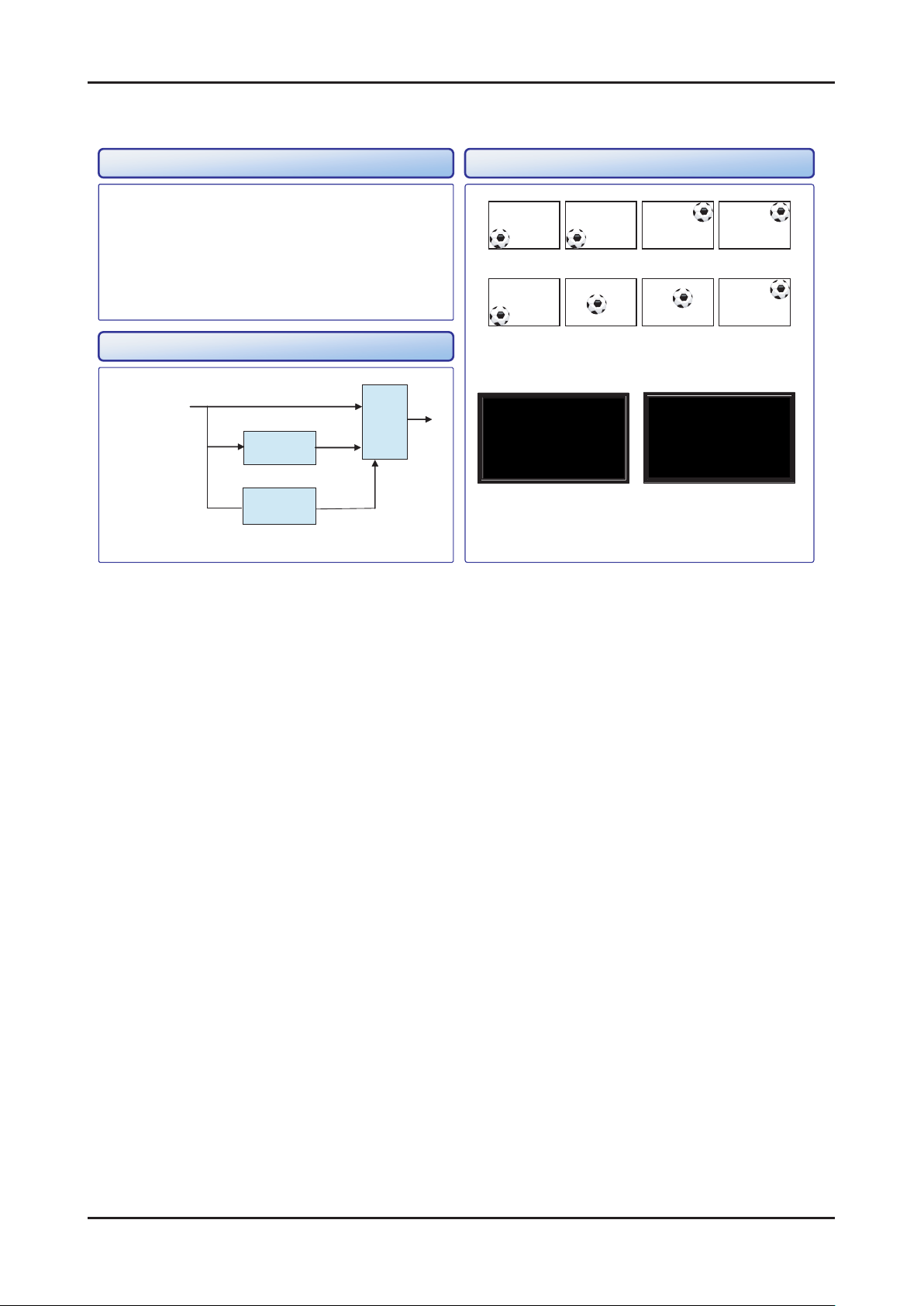
<Motion Judder>
<Motion Judder Cancellation>
• Motion Judder cancellation for HD film image.
• Adaptive Recursive Search (ARS)
- Implementation IPC/MJC at same time
- Search Range
Horizontal : ± ±
72 Pixel, Vertical :
12 Line
OFF ON
Technology Example
Block Diagram
DTV Signal
Film
Detection
ME
(ARS)
IPC
MJC
<Motion Judder>
<Motion Judder Cancellation>
.
2-2. MJC : Motion Judder Cancellation (FRC)
2-6
Page 14
2. Product specications
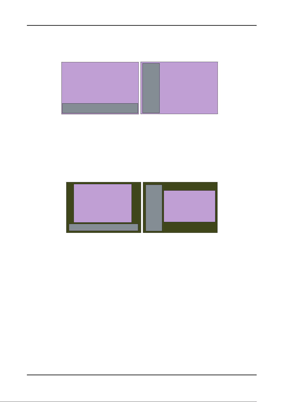
Overlay
(Dock Mode)
Overlay
(Sidebar Mode)
Overlay
(Dock Mode)
Overlay
(Sidebar Mode)
Overlay
(Dock Mode)
Overlay
(Dock Mode)
Overlay
(Sidebar Mode)
Overlay
(Sidebar Mode)
Viewport
(Sidebar Mode)
Viewport
(Dock Mode)
Viewport
(Sidebar Mode)
Viewport
(Dock Mode)
Viewport
(Sidebar Mode)
Viewport
(Sidebar Mode)
Viewport
(Dock Mode)
Viewport
(Dock Mode)
2-3. Internet@TV
2-3-1. Overlay Mode
It offers contents to maximize the benets of the large screen size.
A. In overlay mode, the video plays in its native size, covering up to the full screen.
Graphical elements in the graphical plane are overlaid on top of the video plane.
B. In overlay mode while displaying the sidebar, at least 2/3 of the video is free of graphical overlays.
C. In overlay mode while displaying the dock, at least 3/4 of the video is free of graphical overlays.
D. YahooTV is executed to overlay mode at rst time.
2-3-2. Viewport Mode
A. In viewport mode, the video plays in a scaled-down size, covering only a portion of the screen. This smaller viewing
area for video is called the viewport.
B. The viewport should cover at least half of the screen area. Graphics are displayed in areas outside of the viewport.
C. The purpose of the viewport mode is to display the entire video without obstruction.
D. The viewport mode preserves the 16:9 aspect ratio of the video.
2-7
Page 15

2. Product specications
2-3-3. Yahoo OOBE
Description
A. All users go through OOBE (Guided Setup) to access the dock the rst time.
B. All users must specify a location and accept the TOS before the TV Widgets service are accessible. The rest of the
screens are optional.
C. When user inputs Back button (Return key), TV goes back to the previous screen.
D. IF user input EXIT key, OOBE is goes to hide mode. And user input WIDGET key, previous screen is displayed again.
E. Back Ground of OOBE is TV video.
Start page explain value proposition User must choose country before
TOS is accepted.
Country is sorted by Alphabet.
If user select Up/Down arrow,
Before/Next page is displayed.
2-8
TOS will updated based on country selected. Optional Screen: users are asked to enter
in a prole name. A default name
(Prole One) is given to them if they
do not create a name.
Explanation on proles and security. Optional Yahoo! sign in screens.
Page 16

2. Product specications
Tutorial: Screens explaining how dock works. Tutorial: Screens explaining the sidebar and
global nav buttons.
Final screen before dock comes up.
2-9
Page 17

2. Product specications
2-3-4. Gallery Widget
Overview
A. In the TV Widgets, widget gallery services are online services where widget developers publish widgets for download.
B. The default widget gallery for the platform is the Widget Gallery Services.
C. To nd and install new widgets, launch the gallery widget from the dock.
D. The gallery widget has access to a privileged set of APIs accessible only to Yahoo! signed widgets.
E. These privileged APIs are used to download and install software on your device.
F. Third party widget developers do not have access to these privileged APIs.
G. The gallery widget can potentially be extended by an OEM to connect to one or more widget gallery back-end servers.
H. The Yahoo! Gallery Widget provides the only way to install new widgets from the Widget Gallery Services, which
contain a catalog of 3rd party widgets managed by Yahoo!.
Note: the above image will be updated and visuals elements laid out in this may not apply.
2-10
Page 18

2-3-5. Prole Widget
Overview
2. Product specications
A. The Prole widget is the way to congure your widget environment for your user prole. With the settings
widget you can congure:
i. Prole Management: Create, edit and switch proles.
ii. Security Settings: Setup a Prole and/or Owner PIN for security purposes.
iii. System Settings: Repeat guided setup, set and edit location and restore factory defaults
B. The Prole widget is located in the dock. Press the TV Widget launch key on the remote control to launch the dock,
and then press the RIGHT or LEFT ARROW until you focus on the settings widget.
C. User prole name is displayed on the Prole snippet.
D. Select the Prole snippet to launch the settings widget.
E. The Prole widget opens up into its sidebar.
F. The following functionality is available from the Prole menu:
i. Switch Prole
ii. Settings for Current Prole
iii. System Settings
iv. Administrative Controls
v. Sign-out of Current Prole
2-11
Page 19

2. Product specications
2-3-6. Flickr TV Widget
Description
A. Flickr TV Widget is a Widget for displaying photos from Flickr. You can view your:
i. Personal photos
ii. Your sets of photos
iii. Explore Flickr’s user community photos
iv. Your favorite photos
v. Your contacts’ photos
vi. Your groups
Initial Sidebar View
A. If the user is not signed and user is signed but user has no photo then the default images will be displayed from the
Flickr Explore category.
B. If the user is signed in and the user has 1 photo or more photos, then the photos will be displayed in the top portion of
the Widget Sidebar.
C. The picture layout changes based on the number of photos (1, 2, 3, or 4).
2-12
Page 20

Initial Sidebar View
2. Product specications
A. If the user is not signed and user is signed but user has no photo then the default images will be displayed from the
Flickr Explore category.
B. If the user is signed in and the user has 1 photo or more photos, then the photos will be displayed in the top portion of
the Widget Sidebar.
C. The picture layout changes based on the number of photos (1, 2, 3, or 4).
2-13
Page 21

2. Product specications
2-3-7. Weather Widget
Overview
A. The Weather Widget utilizes the “Tab View” layout of the Widget Sidebar
i. The tab view is a viewable area than contains groups of user interface elements organized under tab headers.
ii. The tab view does not have a page control. Using both tabs and page controls in the same view is prevented
to avoid confusion.
iii. At the top of the tab view is the tab header.
iv. The tab header is designated by a row of slanted buttons, each containing a tab label.
v. A small portion of a slanted button is shown on the far right side of the tab header to indicate that more tabs exist but
are not currently visible.
vi. The tab view uses a carousel design to navigate through each tab.
vii. This means if you navigate past the last tab in the list, the rst tab is displayed again, and the list starts over.
viii. You never reach the end of the tab list.
ix. As you navigate through the tabs by pressing the RIGHT or LEFT ARROWS on the remote control, you will
see all tab headers in the tab carousel before it starts to repeat.
x. The number of tab headers that can be visible depends on each label and the space allotted.
xi. It is recommended that at least two tabs be visible on the initial tab header.
2-3-8. Finance Widget
Overview
A. Yahoo! Finance Icon is displayed on rst time use
B. Snippet will include default set of stock indicators if the user is not logged in nor selected stocks tickers to track then
the following information will be displayed in the snippet
C. The snippet will only display status of one stock symbol at a time
D. The snippet will display the stock symbol, current value, percentage gain/loss, and point gain/loss
2-14
Page 22

2-3-9. News Widget
Overview
A. The News Widget sidebar will then be displayed
B. Several stories will be displayed in the top featured area of the Widget
Navigation will be available to move from one story to the next
i.
ii. These stories are automatically updated by Yahoo!
iii. The feature sections will navigate left and right
iv. Current page number and total pages will be displayed
2. Product specications
2-15
Page 23

2. Product specications
2-4. Using the Content Library
The Content Library allows you to enjoy various content on your TV. You can use the default content
stored in the TV memory or you can enjoy new content using a USB device or via the Internet.
Using the Content Library Menu
1.
Press the MENU button. Press the ▲ or ▼ button to select
Application, then press the ENTER button.
2.
Press the ▲ or ▼ button to select Content Library, then press the
ENTER button.
- The Content Library main menu is displayed.
Press the or button to select an icon (Gallery, Cooking,
3.
Game, Children, Wellness, Other, Content Management),
then press the ENTER button.
Using the Remote Control Button in Content Library Menu
2-16
Page 24

2-5. Using the TV Memory Contents
You can use the default content stored in the TV memory.
You can add/delete the content of the TV memory. To delete/add content, select Content Management.
- To return to Content Library main menu, press the EXIT button
Gallery
This function plays a SlideShow with high resolution images and
background music and produces various atmospheres. Using the
Gallery function of the TV, you can change your home atmosphere.
- The copyrights of the Gallery contents and all issues related to them
are reserved by Gallery Player, Inc.
- Press the ENTERE button to pause the SlideShow, and also
press the ENTERE button to resume the SlideShow.
- Press the INFO button to display the information on the selected
photo. (This is not displayed if the photo has no information.)
2. Product specications
Cooking
You can view various recipes that you can then easily follow step by
step. Enjoy thesecontents which give you great ideas for meals.
- The recipes introduced in the Cooking contents on the Samsung
TV are based on recipes published by Anness Publishing.
- The copyrights of the Cooking contents and all issues related to them
are reserved by Practical Pictures.
Game
This category provides entertainment games for the whole family.
- For the buttons used in the games, refer to the directions on the
screen.
- Color Buttons for Games
Button Operations
Red Press to move to the game home screen
Green Press to pause the game
Yellow Option Key
Blue Press to exit the game
Children
This is educational and interactive content that children can watch
repeatedly.
- The copyrights of the Children contents and issues related to them
reserved by UpToTen.
Wellness
This is benecial health management content that provides stretching
and massage exercises that can be enjoyed by the whole family.
- The Basic Stretches contents are automatically played so that you
can easily follow the movements on the screen.
To move to the previous or next operation, press the
view the required step. The selected item is displayed on the screen.
Others
The default content is not saved in the TV memory.
- You can copy new content to the TV memory using the Content
Management screen.
or button to
2-17
Page 25

2. Product specications
2-6. Using the Content Management
Content Management
You can select multiple content items by selecting content items
repeatedly and pressing the Yellow button.
My Contents
You can check the content saved in the TV memory for each subitem
of the Content Library.
- Select a content item and press the ENTER button.
You can play or delete the selected content item.
USB
You can check the content saved on the USB device for each subitem
of the Content Library.
Select a content item and press the ENTER button.
You can play the selected content item or copy it to the TV memory.
- “Content Library only supports USB Mass Storage Class devices
(MSC). MSC is a Mass Storage Class Bulk-Only Transport device.
Examples of MSC are Thumb drives and Flash Card Readers
(Both USB HDD and HUB are not supported.)
- Playing a game using an external USB memory device will allow
you to save your game (depending on the game). Take care as
removing the USB memory device while saving data to the USB
memory device may cause the data to be lost.
- Downloading New Contents
New content other than the built-in contents will be provided via
the Samsung.com website with or without charge.
Downloading Content
1.
Visit the www.samsung.com website and open the Content Library
page.
2.
Enter the product number (UDN, Unique Device Number).
3.
Select a content item in the Contents Download page.
4.
Download the contents onto the USB memory device.
5.
Go to Content Library main menu by pressing Contents button or
choosing Content Library (Menu → Application → Content Library).
6.
Plug the USB memory into USB port on the side of the TV.
Finding a product number (Unique Device Number, UDN)
1.
Insert the USB memory into the USB port on the side of the TV.
2.
In the USB Browser main screen, press the Green button (Show
UDN).
3.
The 18-digit number on the screen is the product code.
Provided Content
Additional contents are available on www.samsung.com
Setup
- Screen Saver Run Time: Sets the time when the screen saver is run.
- Save UDN: Saves the UDN number to a USB device.
2-18
Page 26

2. Product specications
2-7. Media Play
2-7-1 Using the Media Play Function
This function enables you to view and listen to photo(JPEG), audio les(MP3) and movie(MPEG) saved on a USB Mass
Storage Class (MSC) device.
1.
Press the POWER button on the remote control or front panel.
- The TV is powered on.
2.
Connect a USB device containing JPEG and/or MP3 and or/MPEG
les to the usb jack (USB jack) on the side of the TV.
- (If you enter the Media Play mode with no USB device
connected the message “No external storage device found.
Check the connection status.” will appear. In this case, insert
the USB device, exit the screen by pressing the MEDIA.P
button on the remote control and enter the MEDIA.P screen
again.
- MTP (Media Transfer Protocol) is not supported.
- The le system only supports FAT16/32 (The NTFS le
system is supported).
- Certain types of USB Digital camera and audio devices may
not be compatible with this TV.
- Media Play only supports USB Mass Storage Class devices
(MSC). MSC is a Mass Storage Class Bulk-Only Transport
device. Examples of MSC are Thumb drives and Flash Card
Readers (Both USB HDD and HUB are not supported.)
- Please connect directly to the USB port of your TV. If you are
using a separate cable connection, there may be a USB
Compatibility problem.
-
Before connecting your device to the TV, please back up your
les to prevent them from damage or loss of data.SAMSUNG is
not responsible for any data le damage or data loss.
- Do not disconnect the USB device while it is loading.
- MSC supports MP3 and JPEG les, while a PTP device
supports JPEG les only.
- The sequential jpeg format is supported.
- Photo and audio les must be named in English, French or
Spanish. If not, the les can not be played. Change the le
names to English, French or Spanish if necessary.
- The higher the resolution of the image, the longer it takes to
display on the screen.
- The maximum supported JPEG resolution is 15360 x 8640
pixels.
- For unsupported or corrupted les, the “Not Supported File
Format” message is displayed.
2-19
Page 27

2. Product specications
-. movie format
File Extention Container Video Decoder Resolution Audio codec
Divx 3.11/4.x/5.1/6.0 720 x 576
XviD 1920 x 1080
*.avi AVI
*.mkv MKV
*.asf ASF
*.wmv WMV VC1 1920 x 1080 WMA
*.mp4
*.3gp 3GPP
*.vro
*.mpg
*.mpeg
*.ts
*.tp
*.trp
MP4
(SMP4)
VRO
VOB
PS
TS
H.264 BP/MP/HP 1920 x 1080
MPEG4 SP/ASP 1920 x 1080
Motion JPEG 800 x 600
Divx 3.11/4.x/5.1/6.0 720 x 576
XviD 1920 x 1080
H.264 BP/MP/HP 1920 x 1080
MPEG4 SP/ASP 1920 x 1080
Motion JPEG 800 x 600
Divx 3.11/4.x/5.1/6.0 720 x 576
XviD 1920 x 1080
H.264 BP/MP/HP 1920 x 1080
MPEG4 SP/ASP 1920 x 1080
Motion JPEG 800 x 600
H.264 BP/MP/HP 1920 x 1080
MPEG4 SP/ASP 1920 x 1080
XVID 1920 x 1080
H.264 BP/MP/HP 1920 x 1080
MPEG4 SP/ASP 1920 x 1080
MPEG2 1920 x 1080
MPEG1 1920 x 1080
MPEG2 1920 x 1080
MPEG1 1920 x 1080
MPEG2 1920 x 1080
H.264 1920 x 1080
VC1 1920 x 1080
MP3
AC3
LPCM
ADPCM
MP3
AC3
LPCM
ADPCM
MP3
AC3
LPCM
ADPCM
WMA
MP3
ADPCM
AAC
ADPCM
AAC
AC3, MPEG,
LPCM
AC3, MPEG,
LPCM
AAC
MP3
Support up to MPEG4 GMC 1 Wrapping Point
Support up to H.264 Level 4.0
Support HE-AAC in MP4, 3GPP and TS for DTMB and ISDB-T model
2-20
Page 28

2-8. Spec Comparison to the Old Models
2. Product specications
UB7W
Model
Design
Display Type LCD TV LCD TV
Resolution 1920 x 1080 1920 x 1080
LCD Panel TFT LCD Panel 120Hz TFT LCD Panel 120Hz
Screen Size 40” / 46” / 55” 46” / 52”
Picture ratio 16 : 9 16 : 9
Dimensions
(W x H x D)
((UA40B7000WM/UA46B7000WM/
UA55B7000WM))
39.214 × 10.039 × 27.245 inches _with stand
40
39.214 × 1.177 × 24.804 inches_without stand
44.45 × 10.827 × 30.198 inches_with stand
46
44.45 × 1.177 × 27.757 inches_without stand
55
52 × 12 × 34.529 inches _with stand
52 × 1.177 × 32.088 inches_without stand
(LN46A850S1F/LN52A850S1F)
44.05 x 11.14 x 29.33 inches _with stand
46
44.05 x 1.74 x 27.26 inches _without stand
49.72 x 12.36 x 32.74 inches _with stand
52
49.72 x 1.74 x 30.68 inches _without stand
SAPPHIRE
40
Weight
46
55
Brightness 500 nit 500 nit
Contrast Ratio 3000000:1 50000:1
Picture Enhacer DNIe+(FBE3) DNIe+(FBE3)
Equalizer
Auto Motion Plus
120Hz
Surround Sound 2 Way SRS TruSurround Dolby Digital 2 Way SRS TruSurround Dolby Digital
Speaker Output
Antenna 1 (Cable/Air) 1 (Cable/Air)
40.7 lbs(18.5kg)_with stand
32.56 lbs(14.8kg)_without stand
49.5lbs (22.5kg)_with stand
38.94 lbs(17.7kg)_without stand
60.28lbs (27.4kg)_with stand
48.84 lbs(22.2kg)_without stand
5 Band
YES YES
10W + 10W (40”, 46”)
15W + 15W(55”)
46
52
54.01 lbs(24.5kg)_with stand
45.19 lbs(20.5kg)_without stand
68.78 lbs (31.2kg)_with stand
59.08 lbs (26.8kg)_without stand
5 Band
10W + 10W
2-21
Page 29
2. Product specications
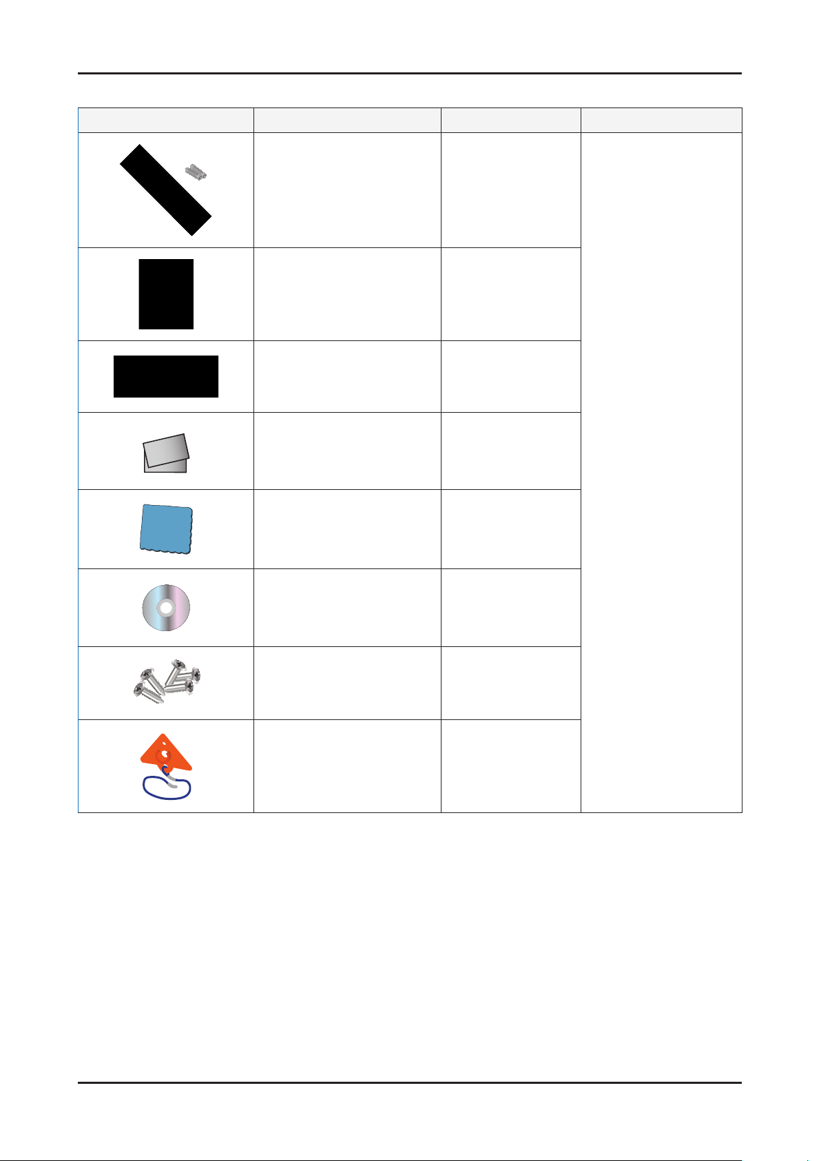
2-9. Accessories
Product Description Code. No Remark
Remote Control & Batteries
(AAA x 2)
Simple Remote Control BN59-00788B
Cover-Bottom BN63-05654B
Warranty Card /
Registration Card /
Safety Guide Manual
(Not available in all location)
Cleaning Cloth BN63-01798B
BN59-00877A
BP68-00263D
Supplied
Accessories
Program CD BN59-00726D
6003-00337
Stand Screw(M4*L10)
Holder-Ring(4ea) BN61-05280A
(UA40B7000,
UA46B7000)
2-22
Page 30

2. Product specications
Product Description Code. No Remark
GENDER CABLE
(COMPONENT)
GENDER CABLE (AV) BN39-01154E
GENDER CABLE
(COMPONENT Sound)
BN39-01154C
BN39-01154G
Supplied
Accessories
2-23
Page 31

3. Disassembly and Reassemble
3. Disassembly and Reassembly
This section of the service manual describes the disassembly and reassembly procedures for the UA40B7000WF LCD TV.
WARNING: This monitor contains electrostatically sensitive devices. Use caution when handling these components.
3-1. Disassembly and Reassembly
Cautions: 1. Disconnect the monitor from the power source before disassembly.
2. Follow these directions carefully; never use metal instruments to pry apart the cabinet.
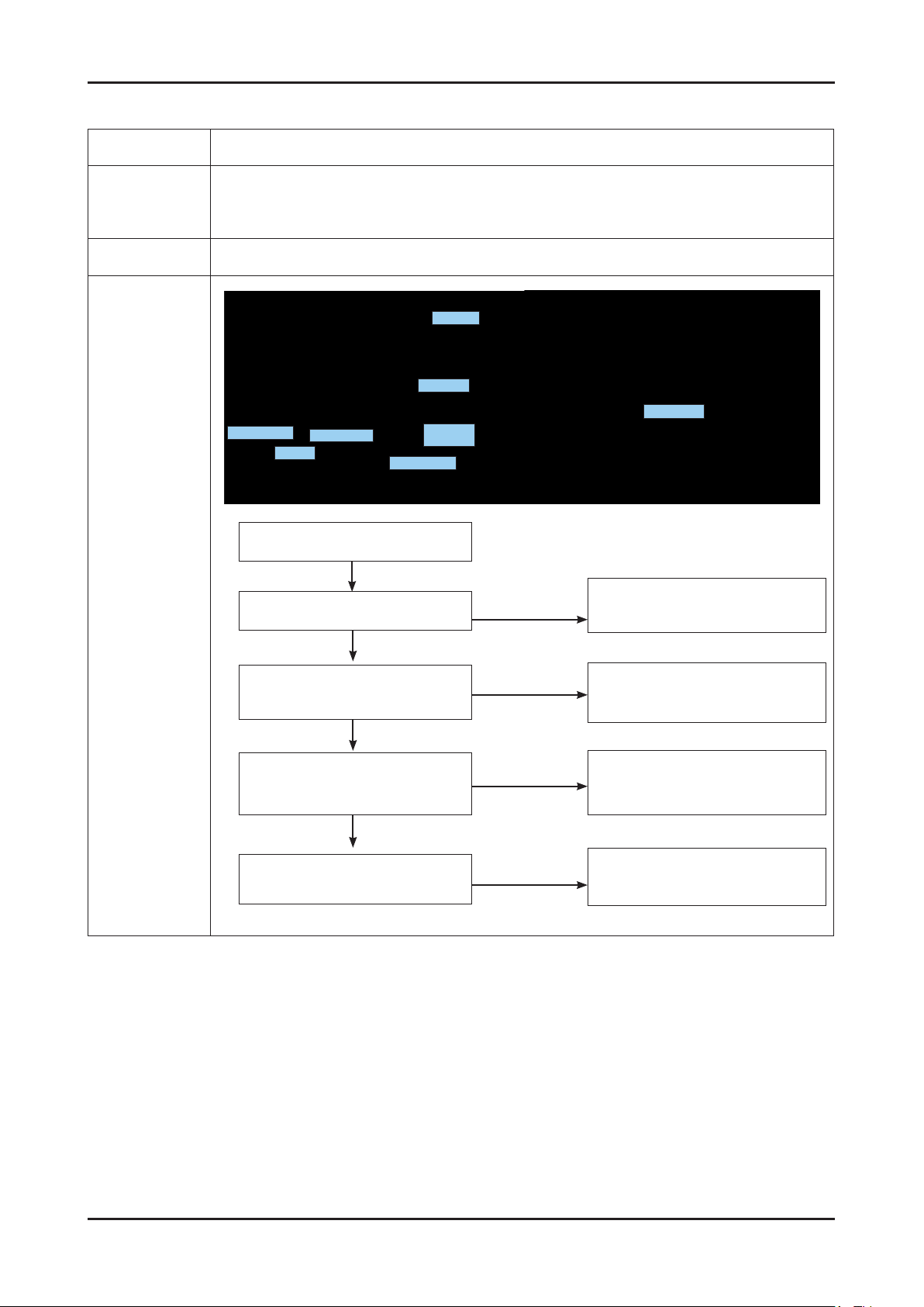
Description Picture Description Screws
1. Place monitor face down on cushioned table.
Remove screws from the Stand.
Remove stand.
3-1
Page 32

3. Disassembly and Reassemble
Description Picture Description Screws
2. Remove the screws of rear-cover. 40”
46”/55”
2-1. Pull out a AC Power Cord
3. Lift up the rear-cover.
3-2
Page 33

3. Disassembly and Reassemble
Description Picture Description Screws
4. Remove the cables and screws from
SMPS, Main board and Woofer and
Bracket stand link.
40”
46” / 55”
Woofer x 2
3-3
Page 34

3. Disassembly and Reassemble
Description Picture Description Screws
5. Remove the panel bracket screws from the
panel.
3-4
Reassembly procedures are in the reverse order of disassembly procedures.※
Page 35

4. Troubleshooting
T-CON
MAIN
SMPS
4. Troubleshooting
4-1. Troubleshooting
1.
Check the various cable connections rst.
• Check to see if there is a burnt or damaged cable.
• Check to see if there is a disconnected or loose cable connection.
• Check to see if the cables are connected according to the connection diagram.
2.
Check the power input to the Main Board.
3.
Check the internal patterns from both the FRC and FBE3 options.
FRC: Factory mode(mute 1 - 8- 2 power on when TV is “standby on “) -> Control -> Test Pattern -> FRC PATT_
BeforeDDR / AfterDDR
* FRCM pattern is created by FRCM IC(T-con)
FBE3: Factory mode(mute 1 - 8- 2 power on when TV is “standby on “) -> Control -> Test Pattern ->FBE Pattern Sel
* Main pattern is created by Main IC(Chelsea)
Case1: FBE3 ok,FRC NG: change the T-con Board
Case2: FBE3 NG, FRC NG: change the main Board
< 46inch model >
* FRCQ : Micronas FRC chip
4-1
Page 36

4. Troubleshooting
Simple ow chart of malfunction
Does the TV turn on?
No
Check the Power Cord
Yes
is any sound of TV
when RF signal
connected?
No
Yes
Can you see anything
on the screen?
Yes
Yes
No
Check LVDS cable connected
Check LVDS
cable connected.
If necessary replace the
T-con board.
Can you see
OSD menu running on
the screen?
No
to Main Board.
If necessary,
replace the Main Board
No
Change the main board.
Yes
Can you see Digital
Channel broadcast ?
No
Replace the Main Board
A5V appear at the
pin 27 of CN1001?
Yes
B13V appear at the
pin 9 of CN1001?
Yes
Please, contact Tech
support
No
No
Check 30p cable.
If necessary, replace the
SMPS board.
Change the main board.
4-2
Page 37

4. Troubleshooting
4-3
Page 38

4. Troubleshooting
Troubelshooting about new functions
I tried to set up BGM in Media play.
I can select a le but I cannot
congure the Mood settings.
I cannot enter Photos, Music or
Movie after running Media play.
Photo thumbnails are not displayed
in the Photo category.
Video thumbnails are not displayed
in the Movie category.
The JPEG les on the USB memory
are not in the list.
I have connected a digital camera,
but I cannot browse the folders.
I cannot play the currently
highlighted le.
I want to know about supported
photo color formats.
I want to know about the maximum
supported photo resolution.
I want to know about supported
music sampling frequencies.
I cannot play MP3 les downloaded
from websites. (Paid MP3 download
sites such as Melon)
I want to know about supported
USB devices.
The supported photo play is slow. An explanation of
I cannot play paid MP3 les. An explanation of
I cannot play a digital camera that
supports PTP.
I cannot use the morning call
function with a digital camera that
supports PTP.
I have changed the device settings
to MSC connection mode after
connecting PTP or during an
operation, but the device is not
recognized.
The WLAN does not work. An explanation of
An explanation of
Media play
An explanation of
Media play
An explanation of
Media play
An explanation of
Media play
An explanation of
Media play
An explanation of
Media play
An explanation of
Media play
An explanation of
Media play
An explanation of
Media play
An explanation of
Media play
An explanation of
Media play
An explanation of
Media play
Media play
Media play
An explanation of
Media play
An explanation of
Media play
An explanation of
Media play
Media play
The BGM shufe and Mood settings are only
available when the Music DB conguration is
complete. Enter the Music category and compelete
the Music DB conguration rst.
Check if the USB memory contains MP3 or JPEG
les.
This may occur when the photo format is not
supported by the TV or the JPEG les do not include
thumbnails.
A video thumbnail is only displayed when the video
has been played at least once.
Files with a path longer than 256 characters will not
be displayed.
When a device is connected in PTP mode, a
browsing folder is not supported.
Check if another le is selected (checked). The
selected le will be played
The RGB, YUV, YCbCr, CMYK, YCCK, GRAY
formats are supported.
The maximum resolution is 15360x8640 pixels.
Supported frequencies are 8, 11.025, 12, 16, 22.05,
24, 32, 44.1, 48 Khz
Playing DRM les (used to protect content) is not
supported.
The TV only supports devices that do not support the
Mass Storage Class or PTP Class.
Devices are not supported when they are connected
to the TV via a USB hub. Supporting USB devices
that require an additional device driver installation is
not guaranteed.
Since the TV does not use caching unlike for a PC,
it make take some time to display a high-resolution
photo.
If the MP3 le is a DRM (Copy Protected) le, the le
will not be played.
Check the PTP mode of the digital camera.
It will not work in Printer Connection mode.
A morning call cannot be set with a PTP device.
Switching the connection mode between MSC and
PTP after a connection is made or during anoperation
is not supported. You can only change the digital
camera connection mode after disconnecting it.
Equipment other than the WLAN USB stick supplied
by Samsung Electronics (as a bundle) will not work.
The sharer must support IEEE 801.11 g/b. IEEE
801.11 n is supported.
4-4
Page 39

4. Troubleshooting
I cannot nd Internet Sharer in the Wlan
settings menu.
The WLAN data rate is slow.
The DLNA server that I could see on the
TV has suddenly disappeared. What
should I do?
Although the Samsung PC server is on,
a message pops up informs you that the
Samsung server is off.
I have registered a le with the
Samsung PC Share Manager to watch
it on the TV, but I cannot nd the le on
the TV. What should I do?
I can see the folders shared through the
PC Share Manager,
but I cannot see the les.
The 2x and 3x Fast Forward video
function on the PC connected to the
network does not work.
Video is played intermittently. DLNA Video Play Check if the network is stable. Check if the network cable is
Pressing the Pause key while a video or
music le is playing does not work. The
Seek function does not work either.
I cannot move folders and les or
cannot copy them by Dragging &
Dropping them in the PC Share
Manager program.
I changed New DTV replacing older
one. However, after changing the DTV,
I can not discover PC Server, though
I use same IP address which I used
before.
I cannot play a video le. DLNA Video Play Only videos recorded by specic Samsung camcorders and
I can see visuals but I cannot hear
audio when playing a video.
An explanation of
Wiselink Pro
An explanation of
Wiselink Pro
PC Share Manager
Search
PC Share Manager
Search
Content Sharing 1. The Share function is not provided for every le. Files in
Content Sharing Since it shows only les corresponding to the Image,
DLNA Video Play The function that supports playing a video on a PC
DLNA Video Play The Pause function may not be supported depending on
PC Share Manager
function
Access control function
runs based solery on
MAC address of target
device.
DLNA Video Play If the audio format is not supported or the le is a non-
Only InfraStructure mode of the sharer is supported.
Ad-Hoc mode is not supported. If multiple sharers are being
used, congure them so that they do not use the same
channel. Set up the sharer to not control the ICMP so that it
answers the Ping test.
If the distance from the sharer is too far, the operation may
slow or the sharer may not be found. If there is an obstacle,
wall or electronic device between the TV and the sharer,
the operation may slow or the sharer may not be found due
to a difculty in communication.
1.Check if the PC is turned off. 2. Check if the Samsung
TV is set to reject connections in the access control menu
of the Samsung PC Share Manager. If so, change the
setting to allow connections. 3.Check if the LAN cable is
connected to the PC and the TV.
When the shared folder of the server is recongured, the
DLNA server function stops temporarily and then resumes
after the reconguration is completed. When the server is
renamed, the DLNA server function also temporarily stops
and then resumes .
a format that is not supported by DLNA are not displayed
on the TV even if they are displayed on a PC. Please
accept our apologies, we are working on this.
2. Check if the folder with the les registered to Samsung
PC Share Manager is shared. The folder should be also
shared.
3. Check if you have clicked the Apply button after sharing
the folder including the le. If you are unsure about this,
please click the button again and recheck if the le is
displayed after a while.
Music, and Movie categories, les that do not correspond
to these categories may not be displayed.
connected over the network does not support the 2x and 3x
Fast Forward functions.
properly connected and if the network is not overloaded.
If there is a wireless network section between the server
and the DTV, the communications environment may be
unstable.
the content provided by the DLNA server or the server.
The Seek function is also not supported.
The PC Share Manager program provides le sharing with
a PC and the TV and does not provide those functions.
You should set new DTV as “accept” in PC share manager
Menu->SHARE->Set Device Policy
digital cameras can be played. Other videos may or may
not be played depending on the resolution and format.
interleaved le, only video is played.
4-5
Page 40

4. Troubleshooting
I cannot play les with the wmv or v
extension.
I cannot use the 20 second Seek
function while playing at 2x Fast
Forward.
Although I can play some les, I cannot
play others even if they have the same
resolution and format.
I can run Trick and Seek with a USB
device, but I cannot run Trick and Seek
with DLNA.
How can I show captions? DLNA Video Play Only the rst language is displayed.
When I enter Internet@TV, the
“Connecting to the service...” warning
message box appears where I can
select either Retry or Cancel, and I
cannot enter Internet@TV. (The Panel
Bar is not displayed.)
Although I can enter Internet@TV, I
cannot connect to the service.
When the network is connected,
I cannot connect to some of the
information.
Photos are not displayed or are
displayed intermittently in the Detailed
News View.
The Mode information of the News
changes. (E.g. ‘Entertainment’ was in
the News mode list, but it has been
removed from the list.)
The displayed stock price is different
from the current price.
DLNA Video Play The video play function is not supported for les with these
extensions.
DLNA Video Play To use the Seek function while playing at 2x Fast Forward,
press the Play button to rst make the playing speed
normal. After that, you will be able to use the Seek function.
DLNA Video Play For unsupported videos, some videos at a certain
resolution and format may be played.
DLNA Video Play For DNLA, Trick is not supported. And only Seek is
supported for PS and TS.
An explanation of
Internet@TV
An explanation of
Internet@TV
An explanation of
Internet@TV
An explanation of
Internet@TV
An explanation of
Internet@TV
An explanation of
Internet@TV
This happens when normal information is not received
from the Internet@TV after purchasing the TV. In this case,
connect the Internet cable and then try again.
This happens when Internet@TV has been properly
connected at least once but the Internet is not currently
connected. In this case, connect the Internet cable and try
again.
This happens when the CP sends incomplete information.
In this case, reconnect to the Internet and try again.
This may occur due to a slow Internet speed. Retry and
ask your Internet Service Provider about the low data rate
problem.
The Mode information of the News is simply displayed as it
is provided by the CP and is not relevant to the TV.
The corresponding information is supplied by CP and is
not relevant to the TV. The information provided by the CP
is delayed information and the announcement informing
the viewer that the information is delayed information is
displayed in the service.
4-6
Page 41

4. Troubleshooting
I want to know how to enter the main
screen.
I want to know how to delete, copy or
move the contents saved on the TV to
an external device.
I have heard that the TV has a
built-in 2GB Flash memory. How can I
access the memory?
I want to perform a SlideShow with
personal photos using the Gallery
function. How can I do this?
When I play a game for the second
time, I want to resume from the last
scene in the previous run. How can I
do this?
Pressing a remote control button while
playing content terminates the current
service and shows the TV Source
screen.
I have heard that the default built-in
content is played by the Adobe ash
player. Therefore, I have downloaded
Flash content from the Internet and
tried to play it from the USB memory
device, but it does not play. What is the
problem?
I want to know how to download and
play new content other than the default
built-in content.
I have downloaded content onto a USB
memory device and inserted the USB
memory into the TV to play the content,
but the TV does not work at all.
Playing fails while playing content
on an external-type USB memory
device.
I can see tiny amounts of alien
substances when I look at the
product edge closely.
An explanation of
Contents Library
An explanation of
Content Library
An explanation of
Content Library
An explanation of
Content Library
An explanation of
Content Library
An explanation of
Content Library
An explanation of
Content Library
An explation of
appearance
Press the [Menu] button, move to [Application] and select
[Contents Library] from the sub menu to enter the main
screen. Alternatively, press the [CONTENT] button from
among the remote control hot keys to enter the main
screen of the corresponding service.
Copying and Moving the default built-in contents is not
supported.
The built-in ash memory within the TV is only installed to
support various TV features, and is not installed for users to
save content. However, you can connect an external-type
USB memory device to the TV and play the contents on the
USB memory.
Images provided by Samsung.com or a 3rd party content
provider linked to Samsung.com will not be played in the
[Contents Library]. However, you can use the SlideShow
function of WiseLink Pro.
The built-in games in the [Contents Library] are basic
casual games that do not support the game saving
function.
Pressing a channel related button on the remote control
shows the TV Source screen. Take care to not press the
Ch Up/Down, Pre. Ch, and Fav. Ch buttons by mistake.
The [Contents Library] does not support playing les
other than the les authorized for playback by Samsung
Electronics or les ofcially provided by a 3rd party content
provider authorized by Samsung Electronics.
New content will be supplied via Samsung.com. The
content supplied by a 3rd party content provider will be
supplied under the responsibility of the corresponding
content provider.
Check if the USB device has been properly connected.
If nothing appears on the screen even if the connection
has been properly connected, enter the main screen of
the Content Library and move to the USB content search
screen by pressing the “Red” color button. If the TV fails
to recognize the USB device, turn the TV off and then on
again, reinsert the USB memory and repeat the above
procedures.
Check the USB connection and try again.
This product has been designed so that the color
appears faint by coating the blank edges with
transparent matter. The substances you see is due to
the design and is not a defect of the product.
4-7
Page 42

4. Troubleshooting
HMDI1/DVI
COMP SOUND
COMPONENT
HDMI2
CN3011
AUDIO
DVI/PC
SOUND IN
HMDI1/DVI
COMP SOUND
COMPONENT
HDMI2
CN3011
AUDIO
DVI/PC
SOUND IN
IC6001IC6001
4-1-1. No Power
The PD board relay does not work when connecting the power cord.
Symptom
Major
checkpoints
Caution Make sure to disconnect the power before working on the IP board.
-
The units appears to be dead.
-
The PD relay does not work when connecting the power cord if the cables are improperly connected or the
Main Board or PD is not functioning. In this case, check the following:
-
Check the internal cable connection status inside the unit.
-
Check the fuses of each part.
-
Check the output voltage of PD.
-
Replace the Main Board.
Diagnostics
When power on, check the sound of
relay on?
Yes
Does proper Stand-By DC
A5V appear at the PIN 27 of CN1001?
Yes
Does proper Main DC B12VS,
B5V,B13V appear at the the PIN23,
PIN15, PIN9 of CN1001?
Yes
Does proper DC A3.3V appear at the
Pin5 of IC1002?
Yes
Does proper DC B3.3V appear at
1pin of IC1005 and IC1008, B9V
appear at 3pin of IC1003?
Yes
Does proper chelsea core 1.2V, 1.8V
appear at C1032, C1033?
Yes
A power is supplied to panel appear
at C7136?
No
No
No
No
No
No
No
Check a connection power cable.
P/N: BN96-09872A
Change the Main Power assembly
40” / 46” : BN44-00269A
55” : BN44-00271A
Change the IC1002 or the Main Assy
Change the IC1005, IC1008, IC1003
or the Main Assy
BN94-02706A
Change the IC1007, IC1008
or the Main Assy
Check a other function (No picture part)
Replace a LCD Panel
40” : BN07-00700B
46” : BN07-00701B
55” : BN07-00702B
4-8
Page 43

4. Troubleshooting
PIN27(A5V)
PIN23(B12VS)
PIN15(B5V)
PIN9(B13V)
4-9
Page 44
4. Troubleshooting
HMDI1/DVI
COMP SOUND
COMPONENT
HDMI2
CN3011
AUDIO
DVI/PC
SOUND IN
HMDI1/DVI
COMP SOUND
COMPONENT
HDMI2
CN3011
AUDIO
DVI/PC
SOUND IN
IC6001IC6001
4-1-2. No Video (Analog PC signal)
Symptom Audio is normal but no picture is displayed on the screen.-
-
Major
checkpoints
Caution Make sure to disconnect the power before working on the IP board.
Check the PC source
-
Check the IC7001(chelsea)
This may happen when the LVDS cable connecting the Main Board and the Panel is disconnected.
-
Diagnostics
No video
Yes
Check the PC source and
check the connection of DSUB?
Yes
Does the signal appear at pin1,2,3,13,14
1
(R,G,B,H,V) of CN3011?
Yes
2
Does the digital data appear
at output of IC6001?
Yes
Check the LVDS cable?
Replace the LCD panel?
No
No
No
No
Input an analog PC signal.
Check the connected cable.
PC cable.
Change the PC cable. Change the main
PCB assembly
Change the IC6001 or the main PCB
assembly
Please, contact Tech support
4-10
Page 45
WAVEFORMS
4. Troubleshooting
1 2
3
PC Input (V-Sync, H-Sync)
LVDS Out (CLK + / -)
4-11
Page 46

4. Troubleshooting
4-1-3. No Video (HDMI - Digital Signal)
Symptom Audio is normal but no picture is displayed on the screen.-
-
Major
checkpoints
Caution Make sure to disconnect the power before working on the IP board.
Check the HDMI source
-
Check the IC7001(chelsea)
This may happen when the LVDS cable connecting the Main Board and the Panel is disconnected.
-
No video
Yes
Check the HDMI source and check
the connection of HDMI cable?
Yes
No
Input an HDMI signal.
Check the connected cable.
Diagnostics
Does the signal appear at IC3013
4
pin2~12(HDMI1), pin14~24(HDMI2),
pin27~37(HDMI3), pin39~49(HDMI4)?
Yes
Dose the digital data appear at output
5
of IC3013 pin89~99(HDMI output)?
Yes
Does the digital data appear at pin
7
14~42 of CN7005?
Yes
Check the LVDS cable?
Check the T-con board?
Replace the LCD panel?
No
No
No
No
Check CN3013, 3016, 3015, 3010
(HDMI1,2,3,4)
Change the HDMI cable, Chagne the
main PCB assembly.
Check IC3013
Change the main PCB assembly
Check IC7001
Change the main PCB assembly
Please, contact Tech support
4-12
Page 47

WAVEFORMS
4. Troubleshooting
4 5
6
HDMI Input (CLK + / -)
Tuner CVBS Out (Pattern: Grey Bar)
7
TS DATA Out (Clk, Data [0])
4-13
Page 48

4. Troubleshooting
4-1-4. No Video (Tuner_CVBS)
Symptom Audio is normal but no picture is displayed on the screen.-
-
Major
checkpoints
Caution Make sure to disconnect the power before working on the IP board.
Check the Tuner CVBS source
-
Check the Chelsea
This may happen when the LVDS cable connecting the Main Board and the Panel is disconnected.
-
Diagnostics
No video
Yes
Check the RF source and
check the connection of RF cable?
Yes
Does the signal appear at pin8 of
6
5
Does the digital data appear at
Check the LVDS cable?
Replace the LCD panel?
TU5001?
Yes
pin14~42 of CN7005?
Yes
No
No
No
No
Input the RF signal.
Check the connected cable.
Check TU5001
Change the main PCB assembly.
Check IC7001
Change the main PCB assembly.
Please, contact Tech support
4-14
Page 49

WAVEFORMS
Tuner CVBS Out (Pattern: Grey Bar)
5
Eagle+ Out (Clk, H-Sync)
6
4. Troubleshooting
4-15
Page 50

4. Troubleshooting
4-1-5. No Video (Tuner DTV)
Symptom Audio is normal but no picture is displayed on the screen.-
-
Major
checkpoints
Caution Make sure to disconnect the power before working on the PD board.
Check the DTV source
-
Check the Chelsea
This may happen when the LVDS cable connecting the Main Board and the Panel is disconnected.
-
Diagnostics
No video
Yes
Check the RF source and
check the connection of RF cable?
Yes
7
5
Does the digital data appear
at pin15, 16 of TU5001?
Yes
Does the digital data appear at
pin14~42 of CN7005?
Yes
Check the LVDS cable?
Replace the LCD panel?
No
No
No
No
Input the RF signal.
Check the connected cable.
Check TU5001
Change the main PCB assembly.
Check IC7001
Change the main PCB assembly.
Please, contact Tech support
4-16
Page 51

WAVEFORMS
Tuner CVBS Out (Pattern: Grey Bar)
5
TS DATA Out (Clk, Data [0])
7
4. Troubleshooting
4-17
Page 52

4. Troubleshooting
CN3001 CN3005 CN3004
CN3011
CN3001 CN3005 CN3004
CN3011
4-1-6. No Video (Video CVBS 1)
Symptom Audio is normal but no picture is displayed on the screen.-
-
Major
checkpoints
Caution Make sure to disconnect the power before working on the PD board.
Check the Video CVBS source
-
Check the Chelsea
This may happen when the LVDS cable connecting the Main Board and the Panel is disconnected.
-
No video
Yes
Diagnostics
Check the video source and
check the connection of
video cable?
Yes
5
Does the signal appear at R3070?
Yes
5
Does the digital data appear at
pin14~42 of CN7005?
Yes
Check the LVDS cable?
Replace the LCD panel?
No
No
No
No
Input a video signal.
Check the connected cable.
Check CN3005
Change the main PCB assy
Check IC7001
Change the main PCB assembly
Please, contact Tech support
4-18
Page 53

WAVEFORMS
Tuner CVBS Out (Pattern: Grey Bar)
5
4. Troubleshooting
4-19
Page 54

4. Troubleshooting
CN3001 CN3005 CN3004
CN3011
CN3001 CN3005 CN3004
CN3011
4-1-7. No Video (Component 1)
Symptom Audio is normal but no picture is displayed on the screen.-
-
Major
checkpoints
Caution Make sure to disconnect the power before working on the PD board.
Check the Component source
-
Check the Chelsea
This may happen when the LVDS cable connecting the Main Board and the Panel is disconnected.
-
No video
Yes
Diagnostics
Check component source and
check the connection of
component cable ?
Yes
Does the signal appear at R3065,
9
R3064, R3066(Y, Pb, Pr)?
Yes
Does the digital data appear at
RA6004, RA6005, RA6006 (Rout)
RA6007, RA6008, RA6009 (Gout)
RA6001, RA6002, RA6003 (Bout)?
Yes
5
Does the digital data appear at
pin14~42 of CN7005?
Yes
Check the LVDS cable?
Replace the LCD panel?
No
No
No
No
No
Input a component signal.
Check the connected cable.
Check CN3004
Change the main PCB assy
Check IC6001
Change the main PCB assembly
Check IC7001
Change the main PCB assembly
Please, contact Tech support
4-20
Page 55

WAVEFORMS
Tuner CVBS Out (Pattern: Grey Bar)
5
Component Input (Y/Pb)
9
4. Troubleshooting
4-21
Page 56

4. Troubleshooting
CN3001 CN3005 CN3004
CN3011
CN3001 CN3005 CN3004
CN3011
4-1-8. No Sound
Symptom Video is normal but there is no sound.-
-
Major
checkpoints
Caution Make sure to disconnect the power before working on the PD board.
When the speaker connectors are disconnected or damaged.
-
When the sound processing part of the Main Board is not functioning.
Speaker defect..
-
No sound
Yes
Diagnostics
Check the sound source and
check the connection of
sound cable?
Yes
Does the signal appear at R3069,
0
R3071?
Yes
!
Does the digital data appear at
pin27,28,29 of IC2002?
Yes
@
Does the signal appear at
pin1~4 of CN2001?
Yes
Check the LVDS cable?
Replace the speaker?
No
No
No
No
No
Input a sound signal.
Check the connected cable.
Check CN3005
Change the main PCB assy
Check IC2001
Change the main PCB assembly
Check IC2002
Change the main PCB assembly
Please, contact Tech support
4-22
Page 57

WAVEFORMS
Audio Input (Sign Wave)
0
I2S Input (Clk, Data)
!
4. Troubleshooting
Audio Amp Out (Sign Wave)
@
4-23
Page 58

4. Troubleshooting
a
b
4-1-10. Reference
Output CNT which run Edge Led
(Is unrelated even if right and left changes)
When you see the screen in front of TV,
If the left side (a) has a problem, Connect 2,
cable at the 1 position, in case of normal picture,
change LED panel.
In case of abnormal picture, check power board.
If the left side (b) has a problem,
Connect 1 cable at the 2 position,
in case of normal picture, change LED panel .
In case of abnormal picture, check power board.
Refer to the picture for matching each LED part of
connector .
however, when pull out pair pins in connector, there
is hardly different So We recommend to change (1)
itself or (2) itself.
4-24
Page 59

Connecting a PC
Using the D-sub cable
Connect a D-Sub Cable between PC IN [PC] connector
1.
on the TV and the PC output connector on your computer
Connect a PC Audio Cable between the PC IN [AUDIO]
2.
jack on the TV and the Audio Out jack of the sound card
on your computer
Using the HDMI/DVI Cable
Connect an HDMI/DVI cable between the HDMI1/DVI
1.
jack on the TV and the PC output jack on your computer.
Connect a PC audio cable between the PC in [AUDIO] jack
2.
on the TV and the Audio Out jack of the sound card on you
computer.
.
4. Troubleshooting
Connecting a DVI
Connect an HDMI/DVI cable between the HDMI1/DVI jack
1.
on the TV and the PC output jack on your device.
Connect a DVI audio cable between the DVI in [AUDIO]
2.
jack on the TV and the Audio Out jack of the sound on you
Device .
* Each PC has a dif
* When connecting a PC, match the color of the connection
terminal to the cable, and PC sound cable from sound card on
your computer.
* When using an HDMI/DVI cable connection, you must use
the HDMI IN 1 terminal and DVI sound cable from your DVI
device.
ferent back panel conguration.
4-25
Page 60

4. Troubleshooting
4-2. Alignments and Adjustments
4-2-1. General Alignment instruction
Usually, a color LCD-TV needs only slight touch-up adjustment upon installation.
1.
Check the basic characteristics such as height, horizontal and vertical sync.
Use the specied test equipment or its equivalent.
2.
Correct impedance matching is essential.
3.
Avoid overload. Excessive signal from a sweep generator might overload the front-end
4.
of the TV. When inserting signal markers, do not allow the marker generator to distort test result.
Connect the TV only to an AC power source with voltage and frequency as specied on
5.
the backcover nameplate.
Do not attempt to connect or disconnect any wire while the TV is turned on. Make sure
6.
that the power cord is disconnected before replacing any parts.
To protect against shock hazard, use an isolation transformer.
7.
4-26
Page 61

4-3. Factory Mode Adjustments
4-3-1 Entering Factory Mode
To enter ‘Service Mode’ Press the remote -control keys in this sequence :
- If you do not have Factory remote - control
4. Troubleshooting
1
8 2 Power OnMUTE
4-3-2 How to Access Service Mode
Using the Customer Remote
Turn the power off and set to stand-by mode
1.
Press the remote buttons in this order; MUTE-1-8-2-Power On to turn the set on.
2.
The set turns on and enters service mode. This may take approximately 20 seconds.
3.
Press the Power button to exit and store data in memory.
4.
- If you fail to enter service mode, repeat steps 1 and 2 above.
Initial SERVICE MODE DISPLAY State
5.
Mode: CDTV . RES : 480I
Option
ADC/WB
Control
Advanced
Buttons operations withn Service Mode
6.
Menu Full Menu Display/Move to Parent Menu
Direction Keys
Direction Keys
Source
Item Selection by Moving the Cursor
/
Data Increase / Decrease for the Selected Item
/
Cycles through the active input source that are connected to the unit
4-27
Page 62

4. Troubleshooting
4-3-3 Factory Data
Option
Main: Opiton, Mode : ATV, RES :480I
Option
ADC/WB
ADC
Factory Reset
Type
Model
TUNER
Region
DDR
Light Effect
Ch Table
Medialink Type
PnP Language
Local Set
PDP GROUP
AV Calibration
Comp Calibration
PC Calibration
HDMI Calibration
40A1UF0E
UB7000
SEC_T
CHI
ON
NONE
Infolink ON
CHI
…
…
Success
Success
Success
Success
ADC Target
1st_AV_Low
1st_AV_High
1st_AV_Delta
1st_COMP_Y_Low
1st_COMP_Cb_Low
1st_COMP_Cr_Low
1st_COMP_Y_High
1st_COMP_Cb_High
1st_COMP_Cr_High
1st_COMP_Delta
1st_PC_R_Low
1st_PC_G_Low
1st_PC_B_Low
1st_PC_R_High
1st_PC_G_High
64
880
1
64
…
…
940
…
…
1
16
…
…
1004
…
1st_PC_B_High
1st_PC_Delta
2nd_AV_R_Low
2nd_AV_G_Low
2nd_AV_B_Low
2nd_AV_R_High
2nd_AV_G_High
2nd_AV_B_High
2nd_AV_Delta
2nd_COMP_R_Low
2nd_COMP_G_Low
2nd_COMP_B_Low
2nd_COMP_R_High
2nd_COMP_G_High
2nd_COMP_B_High
…
1
4
…
…
940
…
…
1
…
…
…
…
…
…
2nd_COMP_Delta
2nd_PC_R_Low
2nd_PC_G_Low
2nd_PC_B_Low
2nd_PC_R_High
2nd_PC_G_High
2nd_PC_B_High
2nd_PC_Delta
2nd_HDMI_R_Low
2nd_HDMI_G_Low
2nd_HDMI_B_Low
2nd_HDMI_R_High
2nd_HDMI_G_High
2nd_HDMI_B_High
2nd_HDMI_Delta
…
…
…
…
…
…
…
…
…
…
…
…
…
…
…
4-28
Page 63

4. Troubleshooting
ADC Result
White Balance
1st_Y_GH
1st_Y_GL
1st_Cb_BH
1st_Cb_BL
1st_Cr_RH
1st_Cr_RL
2nd_R_L
2nd_G_L
2nd_B_L
2nd_R_H
2nd_G_H
2nd_B_H
Sub Brightness
R-Offset
G-Offset
B-Offset
Sub Contrast
R-Gain
G-Gain
B-Gain
Movie R-Offset
Movie B-Offset
Movie R-Gain
Movie B-Gain
249
244
…
…
…
…
131
131
131
108
108
108
128
518
512
506
132
510
512
570
…
…
…
…
EDID
Contol
EDID ON/OFF
EDID WRITE
EDID WRITE PC
EDID WRITE HDMI
EDID WRITE HDMI1
EDID WRITE HDMI2
EDID WRITE HDMI3
EDID WRITE HDMI4
EDID 1.2 PORT
ALL
ON
Success
Success
Success
...
...
...
...
NONE
4-29
Page 64

4. Troubleshooting
Sub Option
RF Mute Time
SUB U-COM
RS-232 Jack
Watchdog
WD COUNT
SSC ON/Off
SSC MRR
SSC MFR
SSC QLC
Gamma
PANEL DISPLAY TIME
Dimm Type
LVDS FORMAT
Language
UI COLOR
PDP Option
Hotel Option
600ms
OFF
UART
ON
0
ON
2
2
4
0.90
10Hr
EXT
VESA
…
RED
HOTEL MODE
POWER ON CHANNEL
POWER ON VOLUME
MIN VOLUME
MAX VOLUME
PANEL BUTTON LOCK
POWER ON SOURCE
TOOLS Support
LNA Support
Wiselink WithOut DB
WiseLink Movie
WiseLink DLNA
WiseLink Write
NETWORK Support
High Devi
Carrier Mute
Volume Curve
PWM MAX
DVOUT CD
CVBS CD
EDID Jack Ident
Info Link Server Type
Info Link Country
OFF
…
…
…
…
…
…
31
1
With DB
ON
ON
ON
Wireless
ON
OFF
EU
256
0
1
OFF
operating
...
TTX List
TTX Group
24P×4 Support
Power Indicator Support
BD Wise Support
RF Remocon Support
Data Service Support
OTA Duration Test
Alternate Del
IIC BUS STOP
Visual Test
Temp Private Range Us
Panel Auto Setting
Checksum
View Log
FontData Viewer
Flof
UserOSD
OFF
ON
ON
OFF
ON
OFF
OFF
OFF
Disable
OFF
Failure
0×0000
Shop Option
Asia Option
Shop Mode
USB DEMO ON(SEC)
USB DEMO OFF(SEC)
Exhibition Mode
PLG_MAX_SHOP
TTX
China HD
NT Conversion
Sepco 120Hz
Unbalance
OFF
OFF
OFF
OFF
130
OFF
OFF
OFF
ON
OFF
4-30
Page 65

4. Troubleshooting
Sound
SAP High Threshold
SAP Low Threshold
Speaker Delay Normal
Auxout Delay Normal
Spdif Delay Normal
Speaker Delay Game
Auxout Delay Game
Spdif Delay Game
STA Amp Vol.
STA Post Scale
STA Speaker EQ
STA Sub Woofer
Mono to Stereo Thld
Stereo to Mono Thld
Pilot Level High Thld
0×30h
0×10h
100
0
0
40
0
0
0×28h
0×7fh
ON
2
0×60h
0×30h
0×70h
Pilot Level Low Thld
A2 Pilot
A2 Pilot AM Carr Low T
NICAM Error High Thld
NICAM Error Low Thld
FM1 CarrMute High Thld
FM1 CarrMute Low Thld
DRC H Thresh
DRC L Thresh
DRC SW Thresh
Chattering Cnt
FM Prescale
AM Prescale
NICAM Prescale
BTSC Mono Prescale
BTSC Stereo Prescale
BTSC Sap Prescale
A2K Prescale
M Prescale
AM Carr High T
0×20h
0×0Ah
0×05h
0×0Eh
0×07h
0×10h
0×08h
0×35h
0×30h
0×3dh
5
20
28
20
…
…
…
…
0
Cong Option
Num of ATV
Num of DTV
Num of AV
Num of SVIDEO
Num of COMP
Num of HDMI
Num of PC
Num of SCART
Num of DVI
Num of OPTICAL Link
Num of MEDIA
Num of PANEL KEY
Num of USB Port
MFT Offset
Select LCD/PDP
HDMI/DVI SEL
Indicator
Wall Mount
Chelsea HV Flip
Num Of Display
1
1
1
0
1
4
1
0
0
0
1
6
2
62.5
LCD
1
ON
OFF
ON
2
HDMI AV MUTE TIME
DVI/HDMI SOUND
HDMI HOT PLUG
HOTPLUG SWITCHING
HOTPLUG OFF HOLD 1
HDMI FL
HDMI FIT CNT LOS
UNST ABLE BAN CNT
HDMI Err Cnt
HDMI ROBIN
HDMI Callback
HDMI CTS Thld
HDMI CTS Cnt1
TMDS_EO2_Boost
TMDS_EO2_Gain
TMDS_PLL_Loop
TMDS_CPREG_BLEED
HDMI EQ
HDMI Switch
TTX Group Delay
DVI SET TIME
W
T CNT SIG
oofer_Type
40
Auto
Disable
Boot
1200ms
200ms
600ms
3500ms
5
ON
OFF
8
1
1
0
3
1
AUTO
SIL9287
OFF
300ms
2
Test Pattern
FPE Pattern Sel
FRC PATT_BeforeDDR
FRC PATT_AfterDDR
LOGIC Pattern Sel
0
0
0
…
4-31
Page 66

4. Troubleshooting
Advanced (Press the 0 button four times on advanced to enters hidden menu)
FBE3
WB Movie W/B MOVIE ON/OFF
BM_slope1
BM_slope2
BM_slope3
BM_slope4
BM_start
BM_start_max
Lfunc_basis
Hfunc_basis
Mean-Offset1
Mean-Offset2
Mean-Slope
ACR-Offset
ACR-th1
ACR-th2
Skin-Enable
MODE
Color Tone
MSub Brightness
MSub Contrast
N_Rgain
N_Bgain
N_Roffset
N_Boffset
W1_Rgain
W1_Bgain
W1_Roffset
W1_Boffset
W2_Rgain
W2_Bgain
19
36
56
75
68
110
70
80
30
235
112
10
10
110
ON
OFF
…
…
…
…
…
…
…
…
…
…
…
…
…
…
Skin-UV
FBE Sub color
M-Skin-UV
M-Sub Color
W2_Rof
W2_Boffset
W3_Rgain
W3_Bgain
W3_Roffset
W3_Boffset
Movie Contrast
Movie Bright
Movie Color
Movie Sharpness
Movie Tint
Movie Backlight
Movie Gamma
M_Sub_Gamma
fset
128
140
…
…
…
…
…
…
…
…
…
…
…
…
…
…
…
…
EPA Standard
4-32
Standard Contrast
Standard Brightness
Standard Sharpness
Standard Color
Standard Tint
Standard Backlight
95
45
50
50
0
5
Page 67

4. Troubleshooting
CH_VDEC
YC_Delay
AGC_mode
Gain_VCR
Y_Gain_Man
Saturation
Hue
Y_Shape_sel
Y_Shape_SCM
C_Shape_sel
C_Shape_SCM
If_iir
If_lt_sel
LTI_en
LTI_level
CTI_en
SCM_STI_EN
V_Delay_adj
U_Delay_adj
1
0
880
128
0
13
29
4
4
0
6
OFF
100
OFF
OFF
0
0
CTI_level
ST_Beg_NTSC
VS_Slice_Level
HS_Slice_Level
FB_Delay_adj
RGB_Delay_adj
h_pk_gain
v_pk_gain
h_pk_band
2d_pk_gain
2d_pk_band
slice_mod_ne
scm_fdet_lvl
bl_range
15
0
4
3
0
0
0
0
0
0
0
44
150
3
AR_ADC
RED_CUTOFF
GREEN_CUTOFF
BLUE_CUT
RED GAIN
GREEN GAIN
BLUE GAIN
PHASE
SOG_BW
SSC_PC
RGB_DLY
OFF
0
0
0
0
0
0
16
3
6
0
4-33
Page 68

4. Troubleshooting
CH_DP
NR
MNR
DCR
SD2HD_DCR
SD2HD_DE
SD2HD_SCL
SD2HD_LTI
SD2HD_NARS
SD2HD_DUR
SD2HD_Metric
Coring_ON_OFF
SD_CSC
HD_CSC
M_SD_CSC
M_HD_CSC
PC_SD_CSC
OFF_Y
OFF_C
OFF_Noise_bias
OFF_YMAX
OFF_FADER
LOW_Y
LOW_C
LOW_Noise_bias
LOW_YMAX
LOW_FADER
MED_Y
MED_C
MED_Noise_bias
MED_YMAX
MED_FADER
OFF
OFF
OFF
OFF
OFF
OFF
0
50
226
OFF
7094
7438
7094
7438
7094
20
6
1
128
180
65
18
1
140
160
80
19
1
155
170
MJC_DBG
MB_STEPS
LIMIT_MV_STEP
GLOBAL_FALLBACK
LOCAL_FALLBACK
HIGH_Y
HIGH_C
HIGH_Noise_bias
HIGH_YMAX
HIGH_FADER
0
72
80
48
5
90
20
1
165
180
Sharpness
4-34
Pre_GainH1
Pre_GainH2
Pre_GainH3
Post_GainH1
Post_GainH2
Post_GainH3
Post_GainV1
Post_GainV2
Post_GainV3
CTI_Gain
Pre_LTIH
SD_TH
HD_TH
NORMAL_LTIH
NORMAL_LTIV
10
15
10
10
15
10
40
50
40
15
4
100
132
8
4
SD_LTIH
SD_LTIV
PRE_CORING
POST_CORING_H
POST_CORING_V
Pre_TOT
Post_TOT
SP Sub Color
16
24
32
32
32
32
32
59
Page 69

4. Troubleshooting
Sharpness_LNA
CE_DIMMING
S1_Pre_GainH1
S1_Pre_GainH2
S1_Pre_GainH3
S1_Post_GainH1
S1_Post_GainH2
S1_Post_GainH3
S1_Post_GainV1
S1_Post_GainV2
S1_Post_GainV3
S2_Pre_GainH1
S2_Pre_GainH2
S2_Pre_GainH3
S2_Post_GainH1
S2_Post_GainH2
S2_Post_GainH3
Contrast Dimming
Dimming in Standard
Dimming in Movie
7
11
11
7
11
11
22
37
30
5
7
7
5
7
7
OFF
ON
ON
S2_Post_GainV1
S2_Post_GainV2
S2_Post_GainV3
S3_Pre_GainH1
S3_Pre_GainH2
S3_Pre_GainH3
S3_Post_GainH1
S3_Post_GainH2
S3_Post_GainH3
S3_Post_GainV1
S3_Post_GainV2
S3_Post_GainV3
15
25
20
2
3
3
2
3
3
7
12
10
LNA_Plus
Synctip_Noise
dB01_th
dB12_th
dB23_th
dB34_th
dB45_th
LNA_Plus_Ylter
413
9
48
73
185
318
3
4-35
Page 70

4. Troubleshooting
Tuner Status
FRC
SNR
BER
Singal Strength
Bandwidth
Frequency
LNA Status
FFT
Modulation
Code Rate
GI
Hier Modulation
Frequency Offset
Timing Offset
AGC
UCB
FRCQ Option
FRCQ Fallback
PLL Type
DEMOD Type
TPS Lock
RS Lock
PQ Others 7.5 IRE NTSC
7.5 IRE OFFSET
HDMI 48Hz Enable
HDMI Black Level
EEPROM RESET
DDR Margin
EER RESET
NVR All Clear OFF
A CTRL_OFFSET_0_3
CTRL_OFFSET_D
A
B CTRL_OFFSET_0_3
B CTRL_OFFSET_D
…
…
OFF
Normal
0×41414141
0×41
0×41410000
0×42
4-36
Page 71

4-4. White Balance - Calibration
4-4-1 White Balance -Calibration
4. Troubleshooting
ADC/WB
4-4-2 Service Adjustment -
Color Calibration
Adjust spec.
1. Source : HDMI
2. Setting Mode : 1280*720@60Hz
3. Pattern : Pattern #24 (Chess Pattern)
ADC
You must perform Calibration in the Lattice Pattern before adjusting the White Balance.
AV Calibration
Comp Calibration
PC Calibration
HDMI Calibration
( Chess Pattern )
4. Use Equipment : CA210 & Master MSPG925 Generator
- Use other equipment only after comparing the result with that of the Master equipment.
Input mode Calibration Pattern
CVBS IN (Model_#3) Perform in NTSC-J B&W Pattern #24 Lattice
Component IN (Model_#6) Perform in 720p B&W Pattern #24 Lattice
PC Analog IN (Model_#21)
HDMI IN Perform in 720p B&W Pattern #24 Lattice
Perform in VESA XGA (1024x768)
B&W Pattern #24
<Table 1>
Lattice
4-37
Page 72

4. Troubleshooting
Method of Color Calibration (AV)
1) Apply the NTSC Lattice (N0.3) pattern signal to the AV IN 1 port
2) Press the Source key to switch to “AV1” mode
3) Enter Service mode
4) Select the “ADC/WB” and “ADB” menu
5) Select the “AV Calibration” menu.
6) In “AV Calibration Off” status, press the “
7) When Calibration is complete, it returns to the high-level menu.
8) You can see the change of the “AV Calibration” status from Failure to Success.
Method of Color Calibration (Component)
1) Apply the 720p Lattice (N0. 6) pattern signal to the Component IN 1 port
2) Press the Source key to switch to “Component1” mode
3) Enter Service mode
4) Select the “ADC/WB” and “ADB” menu
5) Select the “Comp Calibration” menu.
6) In “Comp Calibration Off” status, press the “
7) When Calibration is complete, it returns to the high-level menu.
8) You can see the change of the “Comp Calibration” status from Failure to Success.
Method of Color Calibration (PC)
1) Apply the VESA XGA Lattice (N0. 21) pattern signal to the PC IN port
2) Press the Source key to switch to “PC” mode
3) Enter Service mode
4) Select the “ADC/WB” and “ADB” menu
5) Select the “PC Calibration” menu.
6) In “PC Calibration Off” status, press the “
7) When Calibration is complete, it returns to the high-level menu.
8) You can see the change of the “PC Calibration” status from Failure to Success.
” key to perform Calibration.
” key to perform Calibration.
” key to perform Calibration.
Method of Color Calibration (HDMI)
1) Apply the 720p Lattice (N0. 6) pattern signal to the HDMI1/DVI IN port
2) Press the Source key to switch to “HDMI1” mode
3) Enter Service mode
4) Select the “ADC/WB” and “ADB” menu
5) Select the “HDMI Calibration” menu.
6) In “HDMI Calibration Off” status, press the “
7) When Calibration is complete, it returns to the high-level menu.
8) You can see the change of the “HDMI Calibration” status from Failure to Success.
” key to perform Calibration.
4-38
Page 73

4-4-3 White Balance - Adjustment
4. Troubleshooting
ADC/WB
White Balance
(low light) (hight light)
Sub Bright
R offset
G offset
B offset
(W/B adjustment Condition refer next page)
Sub Contrast
R gain
G gain
B gain
4-5. Servicing Information
4-5-1 Upgrading the Software
Samsung may offer upgrades for TV’s rmware in the future. Please contact the Samsung call center at 1-800-
SAMSUNG (726-7864) to receive information about downloading upgrades and using a USB drive. Upgrades will
be possible by connecting a USB drive to the USB port located on your TV.
Insert a USB drive containing the rmware upgrade
1.
into the Wiselink Pro port on the side of the TV.
If pop up is showed, press the exit or or press the No
2.
button. (If you press Yes button, display is changed to
Wiselink Pro Menu )
Press the MENU button to display the menu.
3.
Press the ▲ or ▼ button to select “Setup”, then press
the ENTER button.
Press the ▲ or ▼ button to select “SW Upgrade”, then
4.
press the ENTER button.
Press the ENTER button.
5.
The message “Scanning for USB... It may take up to 30
seconds.” is displayed.
The message “Upgrade version XXXX to version XXXX?
6.
The system will be reset after upgrade.” is displayed.
Press the ◄ or ► to select the “OK”, then press the
ENTER button.
Please be careful to not disconnect the power or remove
the USB drive while upgrades are being applied. The TV
will turn off and turn on automatically after completing
the rmware upgrade. Please check the rmware version
after the upgrades are complete. When software is
upgraded, video and audio settings you have made will
return to their default (factory) settings.
We recommend you write down your settings so that you
can easily reset them after the upgrade.
4-39
Page 74

4. Troubleshooting
4-5-2 Self Diagnostic
This is simple test function that judge whether is TV SET’s problem or not.
There are two self-test. Picture and Sound.
Press “Menu -> Support -> Self Diagnosis”
1.
The message “Picture Test / Sound Test” is displayed.
2. Picture Test
1) The message “Does the problem still exist with this
test pattern?” is displayed.
2) Press “Yes”. This is a TV SET problem.
The massage “Contact Samsung’s call center at
1-800-SAMSUNG for assistance.” is displayed.
3) Press “No”.
This is not a TV SET problem.
The message “If the self diagnosis picture is OK, picture
distortion may caused by your external device.
Please check connection. If the problem still persists,
refer to the external device’s user manual.” is displayed.
4-40
Page 75

3. Sound Test
1) The message “Does the problem still exist with this
sound test?” is displayed.
2) Press “Yes”. This is a TV SET problem.
The message “Contact Samsung’s call center at
1-800-SAMSUNG for assistance.”is displayed
3) Press “No”.
This is not a TV SET problem.
The message “If the self diagnosis picture is OK, picture
distortion may caused by your external device.
Please check connection. If the problem still persists,
refer to the external device’s user manual.” is displayed.
4. Troubleshooting
4-41
Page 76

5. Exploded View & Part List
T0003
M0215
M0014
M0115
M0027
M0013
BRACKET-AV
ASSY SMPS
T0175
5-1. UA40B7000WM Exploded View
5. Exploded View & Part List
5-1
Page 77
5. Exploded View & Part List
5-1-1. UA40B7000WM Parts List
Location No. Code No. Description & Specication Q’ty S.A/S.N.A Remark
T0003 BN96-09971F ASSY COVER P-FRONT;UB7000 40,PMMA(CLR)+A 1 S.A
M0215 BN07-00700B LCD-PANEL;LTF400HF08 1 S.A
M0215 BN81-02357A A/S-T CON LTF400HF05;LTF400HF05 1 S.N.A
T0175 BN96-11608A ASSY SPEAKER P;8ohm,4pin,15W,R:600,09 LE 1 S.A
T0175 BN96-09470A ASSY SPEAKER P;8ohm,4pin,15W,R:800 / L:8 1 S.A
M0115 BN61-04925A BRACKET-STAND LINK;LB700 40,SECC,T2.0 1 S.N.A
M0014 BN94-02907A ASSY PCB MAIN;UA40B7000WFXXZ,N74A 1 S.N.A
M0013 BN96-09981G ASSY COVER P-REAR;LB7000 40inch,Austrail 1 S.A
M0027 BN96-09474B ASSY STAND P-BASE;40 UB7000,ROSE BLACK,P 1 S.N.A
5-2
Page 78

5-2. UA46B7000WM Exploded View
T0003
M0215
M0014
M0115
M0027
M0013
BRACKET-AV
ASSY SMPS
T0175
5. Exploded View & Part List
5-3
Page 79

5. Exploded View & Part List
5-2-1. UA46B7000WM Parts List
Location No. Code No. Description & Specication Q’ty S.A/S.N.A Remark
T0003 BN96-09972N ASSY COVER P-FRONT;LB7000 46inch,PC(CLR) 1 S.A
M0215 BN07-00701B LCD-PANEL;LTF460HF08 1 S.A
M0215 BN81-02358A A/S-T CON LTF460HF05;LTF460HF05 1 S.N.A
T0175 BN96-09468B ASSY SPEAKER P;8ohm,4pin,Diameter: 120mm 1 S.A
T0175 BN96-09470B ASSY SPEAKER P;8ohm,4pin,15W,R:850 / L:5 1 S.A
M0115 BN61-05536A BRACKET-STAND LINK;LB700 40,SECC,T2.0 1 S.N.A
M0014 BN94-02907B ASSY PCB MAIN;UA46B7000WFXXZ,N74A 1 S.A
M0013 BN96-09977F ASSY COVER P-REAR;LB7000 46inch,PCM T0.5 1 S.A
M0027 BN96-09477B ASSY STAND P-BASE;46 LB7000,PI50 X L96,G 1 S.A
5-4
Page 80

5-3. UA55B7000WM Exploded View
T0003
M0215
M0014
M0115
M0027
M0013
BRACKET-AV
ASSY SMPS
T0175
5. Exploded View & Part List
5-5
Page 81

5. Exploded View & Part List
5-3-1. UA55B7000WM Parts List
Location No. Code No. Description & Specication Q’ty S.A/S.N.A Remark
T0003 BN96-09973P ASSY COVER P-FRONT;LB7000 55inch,PC(CLR) 1 S.A
M0215 BN07-00702B LCD-PANEL;LTF550HF04 1 S.A
M0215 BN81-02362A A/S-T CON LTF550HF03;LTF550HF03 1 S.N.A
T0175 BN96-09470C ASSY SPEAKER P;8ohm,4pin,15W,R:850/L:5 1 S.A
T0175 BN96-09468C ASSY SPEAKER P;8ohm,4pin,Diameter:120mm 1 S.A
M0115 BN61-05536A BRACKET-STAND LINK;UB7000 46inch,HGI,T3.0 1 S.N.A
M0014 BN94-02907B ASSY PCB MAIN;UA55B7000WFXXZ,N74A 1 S.A
M0013 BN96-09974F ASSY COVER P-REAR;LB7000 55inch,PCM T0.5 1 S.A
M0027 BN96-09480B ASSY STAND P-BASE;52 LB7000,PI50 X L96,G 1 S.A
5-6
Page 82

5. Exploded View & Part List
5-4. UA40B7000WM Parts List
Level Location No. Code No. Description & Specication Q’ty SA/SNA Remark
UA40B7000WMXXS
0.1 M0001 BN90-02127F ASSY COVER FRONT;40 B7000 1 S.N.A
..2 T0003 BN96-09971F ASSY COVER P-FRONT;UB7000 40,PMMA(CLR)+A 1 S.A
...3 BN63-01925A FELT-VIBRATION;42D5,FELT,T0.35,10,370 2 S.N.A
...3 CCM1 BN63-02183G COVER-SHEET;Rhcm,PE Vinyl,T0.05,1100mm,2 0.85 S.N.A
...3 CCM1 BN63-05199B COVER-SHEET;AMBER,PE,T0.08,W65mm,200M,CL 2.8 S.N.A
...3 CCM1 BN63-05199F COVER-SHEET;AMBER,PE,T0.08,W95mm,200M,CL 1.2 S.N.A
...3 M0112 BN63-05320F COVER-FRONT;UB7000 40,PMMA(CLEAR)+ABS-PM 1 S.N.A
...3 T0175 BN96-09470A ASSY SPEAKER P;8ohm,4pin,15W,R:800 / L:8 1 S.N.A
...3 BN96-09978B ASSY HOLDER P-BOSS;LB7000 40inch,ABS HB, 1 S.N.A
....4 T0069 AA60-00091E SPACER-FELT;FELT,100X10,BLK,T0.5 1 S.N.A
....4 BN61-04692A BOSS-PRIMER;#94,clear,35cps 0.001 S.N.A
....4 BN61-05236B HOLDER-BOSS BOTTOM;UB7000 40,ABS,BK500,H 1 S.N.A
....4 BN61-03261Z BOSS-TAPE;T1.1,W16,DARK GRAY 3M #4711,VH 0.52 S.N.A
....4 BN61-05728A BOSS-TAPE;UB7000,T0.4,W10,DARK GRAY 0.288 S.N.A
...3 BN96-10736B ASSY BOARD P-TOUCH FUNCTION&PO;LN40B7000 1 S.A
....4 M2893 BN39-01180B LEAD CONNECTOR;UE40B7000WWXXC,UL2835#30, 1 S.A
....4 M2893 BN39-01181A LEAD CONNECTOR;UE40B7000WWXXC,UL1061#28, 1 S.A
....4 M0102 BN96-10732A ASSY BLU P;UE40B7000WWXXC,MB-M0809-RED,R 1 S.N.A
....4 BN96-10735A ASSY BOARD P-TOUCH POWER&IR;LN46B7000WFX 1 S.N.A
....4 M0175 BN96-10736A ASSY BOARD P-TOUCH FUNCTION;LN46B7000WFX 1 S.N.A
...3 T0069 BN60-00120A SPACER-FELT;UB7000 46inch,FELT,L16,T0.5, 4 S.N.A
...3 T0382 BP61-00495C HOLDER-CARE;PJT,ACRYL-FOAM,T0.25,W30.0mm 0.16 S.N.A
...3 T0069 AA60-00091H SPACER-FELT;FELT,150X10,BLK,T1.0 3 S.N.A
...3 T0069 AA60-00091P SPACER-FELT;,FELT,500X10,BLK,T0.5 2 S.N.A
...3 BN64-01022B DECORATION-BOTTOM;UB7000,PC,clear 1 S.N.A
...3 BN61-04661A BRACKET-STOPPER;L650,SK-5,T0.4,Plating,H 4 S.N.A
UA40B7000WM,N74A/40BW1-G7W,40,LCD-TV,SIN
0.1 M0002 BN90-02133F ASSY COVER REAR;UB7000 40 1 S.N.A
..2 C/REAR+PAN 6003-000133 SCREW-TAPTYPE;BH,+,-,S,M4,L8,ZPC(BLK),SW 2 S.N.A
..2 M0013 BN96-09981G ASSY COVER P-REAR;LB7000 40inch,Austrail 1 S.A
...3 T0069 AA60-00091H SPACER-FELT;FELT,150X10,BLK,T1.0 3 S.N.A
...3 M0006 BN63-05321B COVER-REAR;UB7000 40,PCM,T0.5,BKN-P824 1 S.A
...3 T0069 AA63-60131R SPACER-FELT;21Z57,FELT,325,T0.35,7 2 S.N.A
...3 M0131 BN96-10996A ASSY MISC P;LEDTV,40/46 6000/7000 1 S.N.A
....4 T0278 BN60-00122A SPACER-SPONGE;UB7000,CR,L265,T2.0,W10 2 S.N.A
...3 M0279 BN63-00870A FELT;AS17UO,FELT,0.3,10,287 1 S.N.A
..2 T0081 6001-000799 SCREW-MACHINE;BH,+,M3,L5,ZPC(BLK),SWRCH1 3 S.N.A
..2 H/CORD+PAN 6003-000337 SCREW-TAPTYPE;BH,+,S,M4,L10,ZPC(BLK),SWR 1 S.N.A
..2 C/REAR+C/F 6003-001003 SCREW-TAPTYPE;BH,+,B,M4,L12,ZPC(BLK),SWR 12 S.N.A
..2 C/REAR+PAN 6011-001815 BOLT-ETC;M8,L12,ZPC(Black),SWRCH18A,WSP, 4 S.N.A
..2 BN61-04922A HOLDER-CORD;LB7000 46,ABS,V0,BLK 1 S.N.A
0.1 M0216 BN90-02139B ASSY STAND;UB7000 40 1 S.N.A
..2 M0027 BN96-09474B ASSY STAND P-BASE;40 UB7000,ROSE BLACK,P 1 S.N.A
...3 B/S/BOT+G/ 6003-001003 SCREW-TAPTYPE;BH,+,B,M4,L12,ZPC(BLK),SWR 6 S.N.A
...3 G/STAND+G/ 6003-001003 SCREW-TAPTYPE;BH,+,B,M4,L12,ZPC(BLK),SWR 4 S.N.A
5-7
Page 83

5. Exploded View & Part List
Level Location No. Code No. Description & Specication Q’ty SA/SNA Remark
...3 BN61-04731B BOSS-TAPE;AMBER,ACRYL,T1.1,W12.0mm,WHITE 0.95 S.N.A
...3 T0920 BN61-04927A GUIDE-STAND;LB700 46,PET+PC,G/F(15%) V2 1 S.N.A
...3 BN61-05244A BRACKET-SWIVEL BOTTOM;LB700 46,HGI,T3.0 1 S.N.A
...3 BN61-05251A GUIDE-STAND NECK;LB700 46,PC,CLEAR(TP27) 1 S.N.A
....4 BN61-05268A HOLDER-INSERT;46 LB750,PC, EXTRUSION,CLE 1 S.N.A
...3 BN61-05493A HOLDER-SWIVEL RING BOTTOM;LB650 40,Aceta 1 S.N.A
...3 T0056 BN63-05538A COVER-DECORATION;UB7000 46inch,ABS,PMMA, 1 S.N.A
...3 BN63-05632B COVER-STAND GLASS;LB7000 40,GLASS,T8.0,W 1 S.A
...3 CCM1 BN63-04755A COVER-SHEET;AMBER,PE,T0.05,W150mm,200M,6 1.14 S.N.A
...3 M0126 BN73-00215A RUBBER-FOOT;40LB650,RUBBER,15*25,60,4.0, 2 S.N.A
...3 M0126 BN73-00217A RUBBER-FOOT;LB650,RUBBER,DIA30,7.5,Dark 4 S.N.A
...3 BN74-00031A GREASE;kanto-kasei FL-955,grease,wht 0.4 S.N.A
...3 BN61-05240A HOLDER-SWIVEL RING TOP;LB700 46,POM HB,A 1 S.N.A
...3 BN61-05492A BRACKET-STAND BOTTOM;B650 40,SECC,T2.0 1 S.N.A
...3 BN61-04692A BOSS-PRIMER;#94,clear,35cps 0.1 S.N.A
0.1 BN91-03834F ASSY LCD-AMLCD;BN07-00700B,SPVA 82% 1 S.N.A
..2 M0215 BN07-00700B LCD-PANEL;LTF400HF08 1 S.A
...3 BN81-02357A A/S-T CON LTF400HF05;LTF400HF05 1 S.N.A
0.1 M0017 BN91-04097A ASSY CHASSIS;UA40B7000WFXXY 1 S.N.A
..2 M0014 BN94-02873K ASSY PCB MAIN-SQE;UA40B7000WFXXY 1 S.A
...3 T0245 0202-001521 SOLDER-WIRE FLUX;ECO SOLDER RMA98 SUP,D1 0.25 S.N.A
...3 CN3011 3701-001571 CONNECTOR-DSUB;15P,3ROW,FEMALE,ANGLE,TIN 1 S.A
...3 CN906 3707-001090 CONNECTOR-OPTICAL;angle(ULTRA SLIM),SPDI 1 S.A
...3 CN330 3711-003847 HEADER-BOARD TO CABLE;BOX,12P,1R,2mm,ANG 1 S.A
...3 CN1001 3711-005884 HEADER-BOARD TO BOARD;BOX,30P,2R,2mm,ANG 1 S.A
...3 CN330 3711-006715 HEADER-BOARD TO CABLE;BOX,4P,1R,2.5mm,AN 1 S.N.A
...3 CN330 3711-006715 HEADER-BOARD TO CABLE;BOX,4P,1R,2.5mm,AN 1 S.N.A
...3 CN7002_USB 3722-001051 JACK-USB;4P/1C,AU,BLK,ANGLE,A TYPE 1 S.A
...3 CN7006 3722-001051 JACK-USB;4P/1C,AU,BLK,ANGLE,A TYPE 1 S.A
...3 JA330 3722-002844 JACK-PHONE;1/7P,NI,LAUREL-GREEN,ANGLE 1 S.A
...3 JA330 3722-002845 JACK-PHONE;1/7P,NI,YELLOW,ANGLE 1 S.A
...3 JA330 3722-002846 JACK-PHONE;1/6,NI,BLACK,ANGLE 1 S.A
...3 JA330 3722-002846 JACK-PHONE;1/6,NI,BLACK,ANGLE 1 S.A
...3 CN9001_LAN 3722-002849 JACK-MODULAR;8P/8C(ULTRA SLIM),YES,ANGLE 1 S.A
...3 T0562 6046-001015 STAND OFF;#4-40,L5,Ni PLT,C3601,M3 2 S.N.A
...3 CIS3 BN40-00145B TUNER;TDHG6-K13A,TDHG6-K13A,DVB TC,164CH 1 S.A
...3 SUB09 BN61-04923G BRACKET-AV;UB7000 40,PCM,T0.5,BKM-P824,S 1 S.N.A
...3 T0066 BN62-00042A HEAT SINK-ES;30*30*5,Ceramic,T1.5,TAPE 1 S.A
...3 T0066 BN62-00043A HEAT SINK-ES;40*40*5,Ceramic,T1.5,TAPE 1 S.A
...3 T0174 BN97-03426K ASSY SMD;UA40B7000WFXXY,BN94-02873K 1 S.N.A
....4 SUB05 0202-001477 SOLDER-CREAM;LST309-M,D20~45um,96.5Sn/3A 0.384 S.N.A
....4 D2001 0401-001049 DIODE-SWITCHING;LS4148,75V,150mA,SOD-80, 1 S.A
....4 D4003 0401-001049 DIODE-SWITCHING;LS4148,75V,150mA,SOD-80, 1 S.A
....4 D4004 0401-001049 DIODE-SWITCHING;LS4148,75V,150mA,SOD-80, 1 S.A
....4 D4006 0401-001049 DIODE-SWITCHING;LS4148,75V,150mA,SOD-80, 1 S.A
....4 D4100 0401-001049 DIODE-SWITCHING;LS4148,75V,150mA,SOD-80, 1 S.A
....4 D4101 0401-001049 DIODE-SWITCHING;LS4148,75V,150mA,SOD-80, 1 S.A
....4 D4102 0401-001049 DIODE-SWITCHING;LS4148,75V,150mA,SOD-80, 1 S.A
....4 D4228 0401-001049 DIODE-SWITCHING;LS4148,75V,150mA,SOD-80, 1 S.A
5-8
Page 84

5. Exploded View & Part List
Level Location No. Code No. Description & Specication Q’ty SA/SNA Remark
....4 D4229 0401-001049 DIODE-SWITCHING;LS4148,75V,150mA,SOD-80, 1 S.A
....4 D3001 0401-001056 DIODE-SWITCHING;MMBD4148SE,100V,200mA,SO 1 S.A
....4 D3002 0401-001056 DIODE-SWITCHING;MMBD4148SE,100V,200mA,SO 1 S.A
....4 D3051 0401-001056 DIODE-SWITCHING;MMBD4148SE,100V,200mA,SO 1 S.A
....4 D3054 0401-001056 DIODE-SWITCHING;MMBD4148SE,100V,200mA,SO 1 S.A
....4 D3061 0401-001056 DIODE-SWITCHING;MMBD4148SE,100V,200mA,SO 1 S.A
....4 D3062 0401-001056 DIODE-SWITCHING;MMBD4148SE,100V,200mA,SO 1 S.A
....4 D3063 0401-001056 DIODE-SWITCHING;MMBD4148SE,100V,200mA,SO 1 S.A
....4 D3076 0401-001056 DIODE-SWITCHING;MMBD4148SE,100V,200mA,SO 1 S.A
....4 D3077 0401-001056 DIODE-SWITCHING;MMBD4148SE,100V,200mA,SO 1 S.A
....4 D3079 0401-001056 DIODE-SWITCHING;MMBD4148SE,100V,200mA,SO 1 S.A
....4 D3080 0401-001056 DIODE-SWITCHING;MMBD4148SE,100V,200mA,SO 1 S.A
....4 D4008 0401-001056 DIODE-SWITCHING;MMBD4148SE,100V,200mA,SO 1 S.A
....4 D4010 0401-001056 DIODE-SWITCHING;MMBD4148SE,100V,200mA,SO 1 S.A
....4 D9001_LAN 0401-001056 DIODE-SWITCHING;MMBD4148SE,100V,200mA,SO 1 S.A
....4 D9002_LAN 0401-001056 DIODE-SWITCHING;MMBD4148SE,100V,200mA,SO 1 S.A
....4 D9003_LAN 0401-001056 DIODE-SWITCHING;MMBD4148SE,100V,200mA,SO 1 S.A
....4 D9004_LAN 0401-001056 DIODE-SWITCHING;MMBD4148SE,100V,200mA,SO 1 S.A
....4 D5001 0401-001099 DIODE-SWITCHING;1N4148WS,75V,150mA,SOD-3 1 S.N.A
....4 D4001 0403-000002 DIODE-ZENER;VLZ5V6B,5.45/5.73V,500mW,SOD 1 S.A
....4 D5011 0403-000002 DIODE-ZENER;VLZ5V6B,5.45/5.73V,500mW,SOD 1 S.A
....4 D3003 0403-001180 DIODE-ZENER;BZX84C6V2,5.8-6.6V,350mW,SOT 1 S.A
....4 D3004 0403-001180 DIODE-ZENER;BZX84C6V2,5.8-6.6V,350mW,SOT 1 S.A
....4 D3005 0403-001180 DIODE-ZENER;BZX84C6V2,5.8-6.6V,350mW,SOT 1 S.A
....4 D3006 0403-001180 DIODE-ZENER;BZX84C6V2,5.8-6.6V,350mW,SOT 1 S.A
....4 D3007 0403-001180 DIODE-ZENER;BZX84C6V2,5.8-6.6V,350mW,SOT 1 S.A
....4 D3008 0403-001180 DIODE-ZENER;BZX84C6V2,5.8-6.6V,350mW,SOT 1 S.A
....4 D3009 0403-001180 DIODE-ZENER;BZX84C6V2,5.8-6.6V,350mW,SOT 1 S.A
....4 D3011 0403-001180 DIODE-ZENER;BZX84C6V2,5.8-6.6V,350mW,SOT 1 S.A
....4 D3015 0403-001180 DIODE-ZENER;BZX84C6V2,5.8-6.6V,350mW,SOT 1 S.A
....4 D3016 0403-001180 DIODE-ZENER;BZX84C6V2,5.8-6.6V,350mW,SOT 1 S.A
....4 D3018 0403-001180 DIODE-ZENER;BZX84C6V2,5.8-6.6V,350mW,SOT 1 S.A
....4 D3019 0403-001180 DIODE-ZENER;BZX84C6V2,5.8-6.6V,350mW,SOT 1 S.A
....4 D3020 0403-001180 DIODE-ZENER;BZX84C6V2,5.8-6.6V,350mW,SOT 1 S.A
....4 D3021 0403-001180 DIODE-ZENER;BZX84C6V2,5.8-6.6V,350mW,SOT 1 S.A
....4 D3023 0403-001180 DIODE-ZENER;BZX84C6V2,5.8-6.6V,350mW,SOT 1 S.A
....4 D3024 0403-001180 DIODE-ZENER;BZX84C6V2,5.8-6.6V,350mW,SOT 1 S.A
....4 D3028 0403-001180 DIODE-ZENER;BZX84C6V2,5.8-6.6V,350mW,SOT 1 S.A
....4 D3029 0403-001180 DIODE-ZENER;BZX84C6V2,5.8-6.6V,350mW,SOT 1 S.A
....4 D3039 0403-001180 DIODE-ZENER;BZX84C6V2,5.8-6.6V,350mW,SOT 1 S.A
....4 D3045 0403-001180 DIODE-ZENER;BZX84C6V2,5.8-6.6V,350mW,SOT 1 S.A
....4 D3056 0403-001180 DIODE-ZENER;BZX84C6V2,5.8-6.6V,350mW,SOT 1 S.A
....4 D3057 0403-001180 DIODE-ZENER;BZX84C6V2,5.8-6.6V,350mW,SOT 1 S.A
....4 D3058 0403-001180 DIODE-ZENER;BZX84C6V2,5.8-6.6V,350mW,SOT 1 S.A
....4 D3060 0403-001180 DIODE-ZENER;BZX84C6V2,5.8-6.6V,350mW,SOT 1 S.A
....4 D3065 0403-001180 DIODE-ZENER;BZX84C6V2,5.8-6.6V,350mW,SOT 1 S.A
....4 D3066 0403-001180 DIODE-ZENER;BZX84C6V2,5.8-6.6V,350mW,SOT 1 S.A
....4 D3067 0403-001180 DIODE-ZENER;BZX84C6V2,5.8-6.6V,350mW,SOT 1 S.A
....4 D3068 0403-001180 DIODE-ZENER;BZX84C6V2,5.8-6.6V,350mW,SOT 1 S.A
....4 D3069 0403-001180 DIODE-ZENER;BZX84C6V2,5.8-6.6V,350mW,SOT 1 S.A
....4 D3073 0403-001180 DIODE-ZENER;BZX84C6V2,5.8-6.6V,350mW,SOT 1 S.A
5-9
Page 85

5. Exploded View & Part List
Level Location No. Code No. Description & Specication Q’ty SA/SNA Remark
....4 D3074 0403-001180 DIODE-ZENER;BZX84C6V2,5.8-6.6V,350mW,SOT 1 S.A
....4 D3075 0403-001180 DIODE-ZENER;BZX84C6V2,5.8-6.6V,350mW,SOT 1 S.A
....4 D3776 0403-001180 DIODE-ZENER;BZX84C6V2,5.8-6.6V,350mW,SOT 1 S.A
....4 D3779 0403-001180 DIODE-ZENER;BZX84C6V2,5.8-6.6V,350mW,SOT 1 S.A
....4 D0254 0404-001404 DIODE-SCHOTTKY;BAT721C,40V,200mA,SOT-23, 1 S.A
....4 D0254 0404-001404 DIODE-SCHOTTKY;BAT721C,40V,200mA,SOT-23, 1 S.A
....4 D0254 0404-001404 DIODE-SCHOTTKY;BAT721C,40V,200mA,SOT-23, 1 S.A
....4 D0254 0404-001404 DIODE-SCHOTTKY;BAT721C,40V,200mA,SOT-23, 1 S.A
....4 D7001_USB 0406-001200 DIODE-TVS;RCLAMP0504F,6/-/-V,150W,SC-70 1 S.A
....4 D7002 0406-001200 DIODE-TVS;RCLAMP0504F,6/-/-V,150W,SC-70 1 S.A
....4 D3901 0406-001271 DIODE-TVS;RCLAMP0524P,6/-/-V,150W,SLP251 1 S.A
....4 D3902 0406-001271 DIODE-TVS;RCLAMP0524P,6/-/-V,150W,SLP251 1 S.A
....4 D3903 0406-001271 DIODE-TVS;RCLAMP0524P,6/-/-V,150W,SLP251 1 S.A
....4 D3904 0406-001271 DIODE-TVS;RCLAMP0524P,6/-/-V,150W,SLP251 1 S.A
....4 D3905 0406-001271 DIODE-TVS;RCLAMP0524P,6/-/-V,150W,SLP251 1 S.A
....4 D3906 0406-001271 DIODE-TVS;RCLAMP0524P,6/-/-V,150W,SLP251 1 S.A
....4 D3907 0406-001271 DIODE-TVS;RCLAMP0524P,6/-/-V,150W,SLP251 1 S.A
....4 D3908 0406-001271 DIODE-TVS;RCLAMP0524P,6/-/-V,150W,SLP251 1 S.A
....4 D7999 0407-000114 DIODE-SWITCHING;KDS184,80V,100mA,SOT-23, 1 S.N.A
....4 Q4003 0501-000280 TR-SMALL SIGNAL;KSA1182,PNP,150MW,SOT-23 1 S.A
....4 Q4005 0501-000280 TR-SMALL SIGNAL;KSA1182,PNP,150MW,SOT-23 1 S.A
....4 Q4020 0501-000280 TR-SMALL SIGNAL;KSA1182,PNP,150MW,SOT-23 1 S.A
....4 Q1002_LCD 0501-000445 TR-SMALL SIGNAL;KTC3875S-Y,NPN,150mW,SOT 1 S.A
....4 Q1005_LCD 0501-000445 TR-SMALL SIGNAL;KTC3875S-Y,NPN,150mW,SOT 1 S.A
....4 Q3007 0501-000445 TR-SMALL SIGNAL;KTC3875S-Y,NPN,150mW,SOT 1 S.A
....4 Q3008 0501-000445 TR-SMALL SIGNAL;KTC3875S-Y,NPN,150mW,SOT 1 S.A
....4 Q4004 0501-000445 TR-SMALL SIGNAL;KTC3875S-Y,NPN,150mW,SOT 1 S.A
....4 Q4009 0501-000445 TR-SMALL SIGNAL;KTC3875S-Y,NPN,150mW,SOT 1 S.A
....4 Q4011 0501-000445 TR-SMALL SIGNAL;KTC3875S-Y,NPN,150mW,SOT 1 S.A
....4 Q9001_LAN 0501-000445 TR-SMALL SIGNAL;KTC3875S-Y,NPN,150mW,SOT 1 S.A
....4 Q7601_LCD 0501-002080 TR-SMALL SIGNAL;2SC2412K,NPN,200mW,SC-59 1 S.A
....4 Q7602_LCD 0501-002080 TR-SMALL SIGNAL;2SC2412K,NPN,200mW,SC-59 1 S.A
....4 Q409 0505-001916 FET-SILICON;Si4800BDY,N,30V,9A,0.03ohm,2 1 S.A
....4 IC104 0801-002095 IC-CMOS LOGIC;74LCX245,TRANSCEIVER,TSSOP 1 S.A
....4 IC104 0801-002172 IC-CMOS LOGIC;74LCX16244,BUFFER/LINE DRI 1 S.A
....4 IC104 0801-002172 IC-CMOS LOGIC;74LCX16244,BUFFER/LINE DRI 1 S.A
....4 IC104 0801-002630 IC-CMOS LOGIC;74AHCT1G08,2-INPUT AND GAT 1 S.A
....4 IC104 0801-002780 IC-CMOS LOGIC;74LVC1G17,SCHMITT-TRIGGER 1 S.N.A
....4 IC7008 1001-000164 IC-ANALOG MULTIPLEX;74HC4052,CMOS,SOP,16 1 S.A
....4 IC9003_LAN 1001-001109 IC-ANALOG SWITCH;FST3125M,BUS SWITCH & C 1 S.A
....4 IC106 1001-001177 IC-VIDEO SWITCH;TEA6425D,VIDEO SWITCH,SO 1 S.A
....4 IC106 1001-001573 IC-VIDEO SWITCH;SiI9287BCNUTR,QFN,72P,10 1 S.A
....4 IC107 1002-001482 IC-D/A CONVERTER;WM8521H9GED/R,16bit,SOI 1 S.A
....4 IC3001 1006-001266 IC-LINE TRANSCEIVER;3232,TSSOP,16P,174MI 1 S.A
....4 IC112 1103-000129 IC-EEPROM;24C02,2Kbit,256x8,SOP,8P,5x4mm 1 S.A
....4 IC112 1103-000129 IC-EEPROM;24C02,2Kbit,256x8,SOP,8P,5x4mm 1 S.A
....4 IC112 1103-001385 IC-EEPROM;AT24C256,256Kbit,32Kx8,SOP,8P, 1 S.A
....4 IC112 1103-001415 IC-EEPROM;AT93C46D,1Kbit,128x8/64x16,SOP 1 S.N.A
....4 IC7003 1105-001859 IC-DDR2 SDRAM;K4T1G164QD-ZCE7,DDR2,1Gbit 1 S.A
....4 IC7004 1105-001859 IC-DDR2 SDRAM;K4T1G164QD-ZCE7,DDR2,1Gbit 1 S.A
....4 IC7005 1105-001859 IC-DDR2 SDRAM;K4T1G164QD-ZCE7,DDR2,1Gbit 1 S.A
5-10
Page 86

5. Exploded View & Part List
Level Location No. Code No. Description & Specication Q’ty SA/SNA Remark
....4 IC7006 1105-001859 IC-DDR2 SDRAM;K4T1G164QD-ZCE7,DDR2,1Gbit 1 S.A
....4 IC7999 1107-001740 IC-NAND FLASH;KFH8GH6U4M-DIB6,8Gbit,512M 1 S.A
....4 T0124 1201-002796 IC-POWER AMP;STA339BWS,PSSO,36P,10.3x7.5 1 S.A
....4 T0124 1201-002796 IC-POWER AMP;STA339BWS,PSSO,36P,10.3x7.5 1 S.A
....4 T0087 1203-001815 IC-POSI.FIXED REG.;78M09,TO-252,3P,PLAST 1 S.A
....4 T0087 1203-001816 IC-POSI.FIXED REG.;78M08,TO-252,3P,-,PLA 1 S.A
....4 T0087 1203-002842 IC-POSI.FIXED REG.;AP1117D-33A,TO-252,3P 1 S.A
....4 T0087 1203-002842 IC-POSI.FIXED REG.;AP1117D-33A,TO-252,3P 1 S.A
....4 T0087 1203-002898 IC-POSI.FIXED REG.;G950T45R,T0-252,3P,6. 1 S.A
....4 IC012 1203-002995 IC-POSI.ADJUST REG.;AP1117D-A,TO-252,3P, 1 S.A
....4 IC012 1203-002995 IC-POSI.ADJUST REG.;AP1117D-A,TO-252,3P, 1 S.A
....4 IC4005 1203-004363 IC-VOL. DETECTOR;RT9818C-29PV,SOT-23,3P, 1 S.A
....4 IC4004 1203-004364 IC-VOL. DETECTOR;RT9818C-42PV,SOT-23,3P, 1 S.A
....4 IC1007 1203-004879 IC-DC/DC CONVERTER;MP8668DL,QFN,14P,3x4m 1 S.A
....4 T0087 1203-005134 IC-POSI.FIXED REG.;RT9167A-33PB,SOT-23-5 1 S.A
....4 IC1006 1203-005538 IC-DC/DC CONVERTER;AOZ1021HAIL,SOP,8P,4. 1 S.A
....4 IC5006 1203-005559 IC-BACKLIGHT DRIVER;MP3302DJ,TSOT23,5P,2 1 S.A
....4 T0087 1203-005713 IC-POSI.FIXED REG.;S-1172B33-E6T1G,HSOP, 1 S.A
....4 T0087 1203-005713 IC-POSI.FIXED REG.;S-1172B33-E6T1G,HSOP, 1 S.A
....4 IC118 1204-003010 IC-VIDEO PROCESS;SDP84,PBGA,324P,23x23mm 1 S.A
....4 IC7001 1204-003011 IC-DECODER;SDP83,PBGA,729P,34x34mm,PLAST 1 S.A
....4 IC9002_LAN 1205-002941 IC-ETHERNET CONTROLLER;RTL8100CSL-LF,LQF 1 S.N.A
....4 IC3011 1205-003201 IC-BUS SWITCH;TC7WB125FK,SSOP,8P,2x2.3mm 1 S.A
....4 IC2001 1205-003352 IC-CODEC;WM8593SEFT/V,TQFP,64P,10x10mm,P 1 S.A
....4 IC8006 1205-003479 IC-SWITCH;TPS2051BDBVR,SOT-23,5P,2.9x1.6 1 S.A
....4 IC7007 1205-003733 IC-SWITCH;AP2191MPG-13,MSOP-8L-EP,8P,2.9 1 S.A
....4 IC7010_USB 1205-003735 IC-SWITCH;AP2151WG-7,SOT25,5P,2.9x1.6mm, 1 S.A
....4 IC5010 1209-001830 IC-PLL;IDT6V10012PGG,TSSOP,20P,6.5x4.4mm 1 S.A
....4 D4110 1405-001185 VARISTOR;24Vdc,1.6x0.8x0.36mm,TP 1 S.A
....4 D3010 1405-001233 VARISTOR;30Vdc,5A,1.6x0.8x0.8mm,TP 1 S.A
....4 D3012 1405-001233 VARISTOR;30Vdc,5A,1.6x0.8x0.8mm,TP 1 S.A
....4 D3013 1405-001233 VARISTOR;30Vdc,5A,1.6x0.8x0.8mm,TP 1 S.A
....4 D3014 1405-001233 VARISTOR;30Vdc,5A,1.6x0.8x0.8mm,TP 1 S.A
....4 D3017 1405-001233 VARISTOR;30Vdc,5A,1.6x0.8x0.8mm,TP 1 S.A
....4 D3025 1405-001233 VARISTOR;30Vdc,5A,1.6x0.8x0.8mm,TP 1 S.A
....4 D3026 1405-001233 VARISTOR;30Vdc,5A,1.6x0.8x0.8mm,TP 1 S.A
....4 D3027 1405-001233 VARISTOR;30Vdc,5A,1.6x0.8x0.8mm,TP 1 S.A
....4 D3041 1405-001233 VARISTOR;30Vdc,5A,1.6x0.8x0.8mm,TP 1 S.A
....4 D3059 1405-001233 VARISTOR;30Vdc,5A,1.6x0.8x0.8mm,TP 1 S.A
....4 D3064 1405-001233 VARISTOR;30Vdc,5A,1.6x0.8x0.8mm,TP 1 S.A
....4 D3070 1405-001233 VARISTOR;30Vdc,5A,1.6x0.8x0.8mm,TP 1 S.A
....4 D3071 1405-001233 VARISTOR;30Vdc,5A,1.6x0.8x0.8mm,TP 1 S.A
....4 D3072 1405-001233 VARISTOR;30Vdc,5A,1.6x0.8x0.8mm,TP 1 S.A
....4 D3078 1405-001233 VARISTOR;30Vdc,5A,1.6x0.8x0.8mm,TP 1 S.A
....4 D3081 1405-001233 VARISTOR;30Vdc,5A,1.6x0.8x0.8mm,TP 1 S.A
....4 D4011 1405-001233 VARISTOR;30Vdc,5A,1.6x0.8x0.8mm,TP 1 S.A
....4 D4012 1405-001233 VARISTOR;30Vdc,5A,1.6x0.8x0.8mm,TP 1 S.A
....4 D4014 1405-001233 VARISTOR;30Vdc,5A,1.6x0.8x0.8mm,TP 1 S.A
....4 D4016 1405-001233 VARISTOR;30Vdc,5A,1.6x0.8x0.8mm,TP 1 S.A
....4 D4017 1405-001233 VARISTOR;30Vdc,5A,1.6x0.8x0.8mm,TP 1 S.A
....4 D4018 1405-001233 VARISTOR;30Vdc,5A,1.6x0.8x0.8mm,TP 1 S.A
5-11
Page 87

5. Exploded View & Part List
Level Location No. Code No. Description & Specication Q’ty SA/SNA Remark
....4 D7003_USB 1405-001233 VARISTOR;30Vdc,5A,1.6x0.8x0.8mm,TP 1 S.A
....4 D7004 1405-001233 VARISTOR;30Vdc,5A,1.6x0.8x0.8mm,TP 1 S.A
....4 D9005_LAN 1405-001233 VARISTOR;30Vdc,5A,1.6x0.8x0.8mm,TP 1 S.A
....4 D9006_LAN 1405-001233 VARISTOR;30Vdc,5A,1.6x0.8x0.8mm,TP 1 S.A
....4 R7120 2007-000043 R-CHIP;1Kohm,1%,1/10W,TP,1608 1 S.A
....4 R7121 2007-000043 R-CHIP;1Kohm,1%,1/10W,TP,1608 1 S.A
....4 R7122 2007-000043 R-CHIP;1Kohm,1%,1/10W,TP,1608 1 S.A
....4 R7123 2007-000043 R-CHIP;1Kohm,1%,1/10W,TP,1608 1 S.A
....4 R7152 2007-000043 R-CHIP;1Kohm,1%,1/10W,TP,1608 1 S.A
....4 R7153 2007-000043 R-CHIP;1Kohm,1%,1/10W,TP,1608 1 S.A
....4 R7154 2007-000043 R-CHIP;1Kohm,1%,1/10W,TP,1608 1 S.A
....4 R7155 2007-000043 R-CHIP;1Kohm,1%,1/10W,TP,1608 1 S.A
....4 R7162 2007-000043 R-CHIP;1Kohm,1%,1/10W,TP,1608 1 S.A
....4 R7163 2007-000043 R-CHIP;1Kohm,1%,1/10W,TP,1608 1 S.A
....4 R7164 2007-000043 R-CHIP;1Kohm,1%,1/10W,TP,1608 1 S.A
....4 R7165 2007-000043 R-CHIP;1Kohm,1%,1/10W,TP,1608 1 S.A
....4 R7169 2007-000043 R-CHIP;1Kohm,1%,1/10W,TP,1608 1 S.A
....4 R7170 2007-000043 R-CHIP;1Kohm,1%,1/10W,TP,1608 1 S.A
....4 R7171 2007-000043 R-CHIP;1Kohm,1%,1/10W,TP,1608 1 S.A
....4 R7172 2007-000043 R-CHIP;1Kohm,1%,1/10W,TP,1608 1 S.A
....4 R5034 2007-000060 R-CHIP;100Kohm,1%,1/10W,TP,1608 1 S.N.A
....4 R5038 2007-000060 R-CHIP;100Kohm,1%,1/10W,TP,1608 1 S.N.A
....4 R1801 2007-000070 R-CHIP;0ohm,5%,1/10W,TP,1608 1 S.N.A
....4 R5101 2007-000070 R-CHIP;0ohm,5%,1/10W,TP,1608 1 S.N.A
....4 R2058 2007-000072 R-CHIP;47ohm,5%,1/10W,TP,1608 1 S.N.A
....4 R2059 2007-000072 R-CHIP;47ohm,5%,1/10W,TP,1608 1 S.N.A
....4 R2060 2007-000072 R-CHIP;47ohm,5%,1/10W,TP,1608 1 S.N.A
....4 R2061 2007-000072 R-CHIP;47ohm,5%,1/10W,TP,1608 1 S.N.A
....4 R2086_WF 2007-000072 R-CHIP;47ohm,5%,1/10W,TP,1608 1 S.N.A
....4 R2087_WF 2007-000072 R-CHIP;47ohm,5%,1/10W,TP,1608 1 S.N.A
....4 R5112 2007-000074 R-CHIP;100ohm,5%,1/10W,TP,1608 1 S.A
....4 R2085_WF 2007-000090 R-CHIP;10Kohm,5%,1/10W,TP,1608 1 S.A
....4 R7050 2007-000137 R-CHIP;2Kohm,5%,1/16W,TP,1005 1 S.N.A
....4 R7053 2007-000137 R-CHIP;2Kohm,5%,1/16W,TP,1005 1 S.N.A
....4 R7056 2007-000137 R-CHIP;2Kohm,5%,1/16W,TP,1005 1 S.N.A
....4 R7058 2007-000137 R-CHIP;2Kohm,5%,1/16W,TP,1005 1 S.N.A
....4 R7062 2007-000137 R-CHIP;2Kohm,5%,1/16W,TP,1005 1 S.N.A
....4 R7066 2007-000137 R-CHIP;2Kohm,5%,1/16W,TP,1005 1 S.N.A
....4 R7069 2007-000137 R-CHIP;2Kohm,5%,1/16W,TP,1005 1 S.N.A
....4 R7070 2007-000137 R-CHIP;2Kohm,5%,1/16W,TP,1005 1 S.N.A
....4 R2001 2007-000138 R-CHIP;100ohm,5%,1/16W,TP,1005 1 S.N.A
....4 R2002 2007-000138 R-CHIP;100ohm,5%,1/16W,TP,1005 1 S.N.A
....4 R2025 2007-000138 R-CHIP;100ohm,5%,1/16W,TP,1005 1 S.N.A
....4 R2026 2007-000138 R-CHIP;100ohm,5%,1/16W,TP,1005 1 S.N.A
....4 R3007 2007-000138 R-CHIP;100ohm,5%,1/16W,TP,1005 1 S.N.A
....4 R3034 2007-000138 R-CHIP;100ohm,5%,1/16W,TP,1005 1 S.N.A
....4 R3036 2007-000138 R-CHIP;100ohm,5%,1/16W,TP,1005 1 S.N.A
....4 R3046_AU 2007-000138 R-CHIP;100ohm,5%,1/16W,TP,1005 1 S.N.A
....4 R3062 2007-000138 R-CHIP;100ohm,5%,1/16W,TP,1005 1 S.N.A
....4 R3068 2007-000138 R-CHIP;100ohm,5%,1/16W,TP,1005 1 S.N.A
....4 R3070 2007-000138 R-CHIP;100ohm,5%,1/16W,TP,1005 1 S.N.A
5-12
Page 88

5. Exploded View & Part List
Level Location No. Code No. Description & Specication Q’ty SA/SNA Remark
....4 R3120 2007-000138 R-CHIP;100ohm,5%,1/16W,TP,1005 1 S.N.A
....4 R3205 2007-000138 R-CHIP;100ohm,5%,1/16W,TP,1005 1 S.N.A
....4 R3206 2007-000138 R-CHIP;100ohm,5%,1/16W,TP,1005 1 S.N.A
....4 R3207 2007-000138 R-CHIP;100ohm,5%,1/16W,TP,1005 1 S.N.A
....4 R3243 2007-000138 R-CHIP;100ohm,5%,1/16W,TP,1005 1 S.N.A
....4 R4042 2007-000138 R-CHIP;100ohm,5%,1/16W,TP,1005 1 S.N.A
....4 R4049 2007-000138 R-CHIP;100ohm,5%,1/16W,TP,1005 1 S.N.A
....4 R4050 2007-000138 R-CHIP;100ohm,5%,1/16W,TP,1005 1 S.N.A
....4 R4079 2007-000138 R-CHIP;100ohm,5%,1/16W,TP,1005 1 S.N.A
....4 R4080 2007-000138 R-CHIP;100ohm,5%,1/16W,TP,1005 1 S.N.A
....4 R4087 2007-000138 R-CHIP;100ohm,5%,1/16W,TP,1005 1 S.N.A
....4 R4097 2007-000138 R-CHIP;100ohm,5%,1/16W,TP,1005 1 S.N.A
....4 R4155 2007-000138 R-CHIP;100ohm,5%,1/16W,TP,1005 1 S.N.A
....4 R7114 2007-000138 R-CHIP;100ohm,5%,1/16W,TP,1005 1 S.N.A
....4 R7605_LCD 2007-000138 R-CHIP;100ohm,5%,1/16W,TP,1005 1 S.N.A
....4 R8311 2007-000138 R-CHIP;100ohm,5%,1/16W,TP,1005 1 S.N.A
....4 R1031_LCD 2007-000140 R-CHIP;1Kohm,5%,1/16W,TP,1005 1 S.N.A
....4 R1072 2007-000140 R-CHIP;1Kohm,5%,1/16W,TP,1005 1 S.N.A
....4 R1172 2007-000140 R-CHIP;1Kohm,5%,1/16W,TP,1005 1 S.N.A
....4 R3010 2007-000140 R-CHIP;1Kohm,5%,1/16W,TP,1005 1 S.N.A
....4 R3021 2007-000140 R-CHIP;1Kohm,5%,1/16W,TP,1005 1 S.N.A
....4 R3022 2007-000140 R-CHIP;1Kohm,5%,1/16W,TP,1005 1 S.N.A
....4 R3035 2007-000140 R-CHIP;1Kohm,5%,1/16W,TP,1005 1 S.N.A
....4 R3037 2007-000140 R-CHIP;1Kohm,5%,1/16W,TP,1005 1 S.N.A
....4 R3069 2007-000140 R-CHIP;1Kohm,5%,1/16W,TP,1005 1 S.N.A
....4 R3071 2007-000140 R-CHIP;1Kohm,5%,1/16W,TP,1005 1 S.N.A
....4 R3227 2007-000140 R-CHIP;1Kohm,5%,1/16W,TP,1005 1 S.N.A
....4 R3228 2007-000140 R-CHIP;1Kohm,5%,1/16W,TP,1005 1 S.N.A
....4 R4081 2007-000140 R-CHIP;1Kohm,5%,1/16W,TP,1005 1 S.N.A
....4 R6028 2007-000140 R-CHIP;1Kohm,5%,1/16W,TP,1005 1 S.N.A
....4 R6064 2007-000140 R-CHIP;1Kohm,5%,1/16W,TP,1005 1 S.N.A
....4 R6065 2007-000140 R-CHIP;1Kohm,5%,1/16W,TP,1005 1 S.N.A
....4 R6066 2007-000140 R-CHIP;1Kohm,5%,1/16W,TP,1005 1 S.N.A
....4 R7045 2007-000140 R-CHIP;1Kohm,5%,1/16W,TP,1005 1 S.N.A
....4 R7072 2007-000140 R-CHIP;1Kohm,5%,1/16W,TP,1005 1 S.N.A
....4 R7195 2007-000140 R-CHIP;1Kohm,5%,1/16W,TP,1005 1 S.N.A
....4 R7196 2007-000140 R-CHIP;1Kohm,5%,1/16W,TP,1005 1 S.N.A
....4 R7602_LCD 2007-000140 R-CHIP;1Kohm,5%,1/16W,TP,1005 1 S.N.A
....4 R7999 2007-000140 R-CHIP;1Kohm,5%,1/16W,TP,1005 1 S.N.A
....4 R9007_LAN 2007-000140 R-CHIP;1Kohm,5%,1/16W,TP,1005 1 S.N.A
....4 R2054 2007-000141 R-CHIP;2.2Kohm,5%,1/16W,TP,1005 1 S.N.A
....4 R2081_WF 2007-000141 R-CHIP;2.2Kohm,5%,1/16W,TP,1005 1 S.N.A
....4 R4019 2007-000141 R-CHIP;2.2Kohm,5%,1/16W,TP,1005 1 S.N.A
....4 R4085 2007-000141 R-CHIP;2.2Kohm,5%,1/16W,TP,1005 1 S.N.A
....4 R5030 2007-000141 R-CHIP;2.2Kohm,5%,1/16W,TP,1005 1 S.N.A
....4 R1030_LCD 2007-000143 R-CHIP;4.7Kohm,5%,1/16W,TP,1005 1 S.N.A
....4 R1060 2007-000143 R-CHIP;4.7Kohm,5%,1/16W,TP,1005 1 S.N.A
....4 R1070 2007-000143 R-CHIP;4.7Kohm,5%,1/16W,TP,1005 1 S.N.A
....4 R1170 2007-000143 R-CHIP;4.7Kohm,5%,1/16W,TP,1005 1 S.N.A
....4 R2062 2007-000143 R-CHIP;4.7Kohm,5%,1/16W,TP,1005 1 S.N.A
....4 R2063 2007-000143 R-CHIP;4.7Kohm,5%,1/16W,TP,1005 1 S.N.A
5-13
Page 89

5. Exploded View & Part List
Level Location No. Code No. Description & Specication Q’ty SA/SNA Remark
....4 R3159 2007-000143 R-CHIP;4.7Kohm,5%,1/16W,TP,1005 1 S.N.A
....4 R3272 2007-000143 R-CHIP;4.7Kohm,5%,1/16W,TP,1005 1 S.N.A
....4 R3273 2007-000143 R-CHIP;4.7Kohm,5%,1/16W,TP,1005 1 S.N.A
....4 R3274 2007-000143 R-CHIP;4.7Kohm,5%,1/16W,TP,1005 1 S.N.A
....4 R4016 2007-000143 R-CHIP;4.7Kohm,5%,1/16W,TP,1005 1 S.N.A
....4 R4018 2007-000143 R-CHIP;4.7Kohm,5%,1/16W,TP,1005 1 S.N.A
....4 R4020 2007-000143 R-CHIP;4.7Kohm,5%,1/16W,TP,1005 1 S.N.A
....4 R4057 2007-000143 R-CHIP;4.7Kohm,5%,1/16W,TP,1005 1 S.N.A
....4 R4059 2007-000143 R-CHIP;4.7Kohm,5%,1/16W,TP,1005 1 S.N.A
....4 R4066 2007-000143 R-CHIP;4.7Kohm,5%,1/16W,TP,1005 1 S.N.A
....4 R4074 2007-000143 R-CHIP;4.7Kohm,5%,1/16W,TP,1005 1 S.N.A
....4 R4077 2007-000143 R-CHIP;4.7Kohm,5%,1/16W,TP,1005 1 S.N.A
....4 R4500_AU 2007-000143 R-CHIP;4.7Kohm,5%,1/16W,TP,1005 1 S.N.A
....4 R4501_AU 2007-000143 R-CHIP;4.7Kohm,5%,1/16W,TP,1005 1 S.N.A
....4 R4771 2007-000143 R-CHIP;4.7Kohm,5%,1/16W,TP,1005 1 S.N.A
....4 R4772 2007-000143 R-CHIP;4.7Kohm,5%,1/16W,TP,1005 1 S.N.A
....4 R4773 2007-000143 R-CHIP;4.7Kohm,5%,1/16W,TP,1005 1 S.N.A
....4 R4774 2007-000143 R-CHIP;4.7Kohm,5%,1/16W,TP,1005 1 S.N.A
....4 R5017 2007-000143 R-CHIP;4.7Kohm,5%,1/16W,TP,1005 1 S.N.A
....4 R6015 2007-000143 R-CHIP;4.7Kohm,5%,1/16W,TP,1005 1 S.N.A
....4 R6021 2007-000143 R-CHIP;4.7Kohm,5%,1/16W,TP,1005 1 S.N.A
....4 R6023 2007-000143 R-CHIP;4.7Kohm,5%,1/16W,TP,1005 1 S.N.A
....4 R6038 2007-000143 R-CHIP;4.7Kohm,5%,1/16W,TP,1005 1 S.N.A
....4 R6039 2007-000143 R-CHIP;4.7Kohm,5%,1/16W,TP,1005 1 S.N.A
....4 R6040 2007-000143 R-CHIP;4.7Kohm,5%,1/16W,TP,1005 1 S.N.A
....4 R6048 2007-000143 R-CHIP;4.7Kohm,5%,1/16W,TP,1005 1 S.N.A
....4 R6053 2007-000143 R-CHIP;4.7Kohm,5%,1/16W,TP,1005 1 S.N.A
....4 R6100 2007-000143 R-CHIP;4.7Kohm,5%,1/16W,TP,1005 1 S.N.A
....4 R6101 2007-000143 R-CHIP;4.7Kohm,5%,1/16W,TP,1005 1 S.N.A
....4 R6102 2007-000143 R-CHIP;4.7Kohm,5%,1/16W,TP,1005 1 S.N.A
....4 R7010 2007-000143 R-CHIP;4.7Kohm,5%,1/16W,TP,1005 1 S.N.A
....4 R7011_N6V 2007-000143 R-CHIP;4.7Kohm,5%,1/16W,TP,1005 1 S.N.A
....4 R7012 2007-000143 R-CHIP;4.7Kohm,5%,1/16W,TP,1005 1 S.N.A
....4 R7013 2007-000143 R-CHIP;4.7Kohm,5%,1/16W,TP,1005 1 S.N.A
....4 R7017 2007-000143 R-CHIP;4.7Kohm,5%,1/16W,TP,1005 1 S.N.A
....4 R7033 2007-000143 R-CHIP;4.7Kohm,5%,1/16W,TP,1005 1 S.N.A
....4 R7034 2007-000143 R-CHIP;4.7Kohm,5%,1/16W,TP,1005 1 S.N.A
....4 R7036 2007-000143 R-CHIP;4.7Kohm,5%,1/16W,TP,1005 1 S.N.A
....4 R7037 2007-000143 R-CHIP;4.7Kohm,5%,1/16W,TP,1005 1 S.N.A
....4 R7060 2007-000143 R-CHIP;4.7Kohm,5%,1/16W,TP,1005 1 S.N.A
....4 R7063 2007-000143 R-CHIP;4.7Kohm,5%,1/16W,TP,1005 1 S.N.A
....4 R7064 2007-000143 R-CHIP;4.7Kohm,5%,1/16W,TP,1005 1 S.N.A
....4 R7065 2007-000143 R-CHIP;4.7Kohm,5%,1/16W,TP,1005 1 S.N.A
....4 R7067 2007-000143 R-CHIP;4.7Kohm,5%,1/16W,TP,1005 1 S.N.A
....4 R7068 2007-000143 R-CHIP;4.7Kohm,5%,1/16W,TP,1005 1 S.N.A
....4 R7131 2007-000143 R-CHIP;4.7Kohm,5%,1/16W,TP,1005 1 S.N.A
....4 R7136 2007-000143 R-CHIP;4.7Kohm,5%,1/16W,TP,1005 1 S.N.A
....4 R7137 2007-000143 R-CHIP;4.7Kohm,5%,1/16W,TP,1005 1 S.N.A
....4 R7148_USB 2007-000143 R-CHIP;4.7Kohm,5%,1/16W,TP,1005 1 S.N.A
....4 R7156 2007-000143 R-CHIP;4.7Kohm,5%,1/16W,TP,1005 1 S.N.A
....4 R7174 2007-000143 R-CHIP;4.7Kohm,5%,1/16W,TP,1005 1 S.N.A
5-14
Page 90

5. Exploded View & Part List
Level Location No. Code No. Description & Specication Q’ty SA/SNA Remark
....4 R7239 2007-000143 R-CHIP;4.7Kohm,5%,1/16W,TP,1005 1 S.N.A
....4 R7240 2007-000143 R-CHIP;4.7Kohm,5%,1/16W,TP,1005 1 S.N.A
....4 R7400 2007-000143 R-CHIP;4.7Kohm,5%,1/16W,TP,1005 1 S.N.A
....4 R7401 2007-000143 R-CHIP;4.7Kohm,5%,1/16W,TP,1005 1 S.N.A
....4 R7800 2007-000143 R-CHIP;4.7Kohm,5%,1/16W,TP,1005 1 S.N.A
....4 R3044 2007-000146 R-CHIP;6.8Kohm,5%,1/16W,TP,1005 1 S.N.A
....4 R1013 2007-000148 R-CHIP;10Kohm,5%,1/16W,TP,1005 1 S.N.A
....4 R1015 2007-000148 R-CHIP;10Kohm,5%,1/16W,TP,1005 1 S.N.A
....4 R2023 2007-000148 R-CHIP;10Kohm,5%,1/16W,TP,1005 1 S.N.A
....4 R2027 2007-000148 R-CHIP;10Kohm,5%,1/16W,TP,1005 1 S.N.A
....4 R3168 2007-000148 R-CHIP;10Kohm,5%,1/16W,TP,1005 1 S.N.A
....4 R3252 2007-000148 R-CHIP;10Kohm,5%,1/16W,TP,1005 1 S.N.A
....4 R3253 2007-000148 R-CHIP;10Kohm,5%,1/16W,TP,1005 1 S.N.A
....4 R3310 2007-000148 R-CHIP;10Kohm,5%,1/16W,TP,1005 1 S.N.A
....4 R3311 2007-000148 R-CHIP;10Kohm,5%,1/16W,TP,1005 1 S.N.A
....4 R4017 2007-000148 R-CHIP;10Kohm,5%,1/16W,TP,1005 1 S.N.A
....4 R4023 2007-000148 R-CHIP;10Kohm,5%,1/16W,TP,1005 1 S.N.A
....4 R4027 2007-000148 R-CHIP;10Kohm,5%,1/16W,TP,1005 1 S.N.A
....4 R4078 2007-000148 R-CHIP;10Kohm,5%,1/16W,TP,1005 1 S.N.A
....4 R4150 2007-000148 R-CHIP;10Kohm,5%,1/16W,TP,1005 1 S.N.A
....4 R5111 2007-000148 R-CHIP;10Kohm,5%,1/16W,TP,1005 1 S.N.A
....4 R6847 2007-000148 R-CHIP;10Kohm,5%,1/16W,TP,1005 1 S.N.A
....4 R7103 2007-000148 R-CHIP;10Kohm,5%,1/16W,TP,1005 1 S.N.A
....4 R7351 2007-000148 R-CHIP;10Kohm,5%,1/16W,TP,1005 1 S.N.A
....4 R7411_LCD 2007-000148 R-CHIP;10Kohm,5%,1/16W,TP,1005 1 S.N.A
....4 R7600_LCD 2007-000148 R-CHIP;10Kohm,5%,1/16W,TP,1005 1 S.N.A
....4 R7601_LCD 2007-000148 R-CHIP;10Kohm,5%,1/16W,TP,1005 1 S.N.A
....4 R7603_LCD 2007-000148 R-CHIP;10Kohm,5%,1/16W,TP,1005 1 S.N.A
....4 R7604_LCD 2007-000148 R-CHIP;10Kohm,5%,1/16W,TP,1005 1 S.N.A
....4 R8012 2007-000148 R-CHIP;10Kohm,5%,1/16W,TP,1005 1 S.N.A
....4 R8014 2007-000148 R-CHIP;10Kohm,5%,1/16W,TP,1005 1 S.N.A
....4 R8015 2007-000148 R-CHIP;10Kohm,5%,1/16W,TP,1005 1 S.N.A
....4 R8020 2007-000148 R-CHIP;10Kohm,5%,1/16W,TP,1005 1 S.N.A
....4 R8022 2007-000148 R-CHIP;10Kohm,5%,1/16W,TP,1005 1 S.N.A
....4 R8023 2007-000148 R-CHIP;10Kohm,5%,1/16W,TP,1005 1 S.N.A
....4 R9028_LAN 2007-000148 R-CHIP;10Kohm,5%,1/16W,TP,1005 1 S.N.A
....4 R4021 2007-000155 R-CHIP;27Kohm,5%,1/16W,TP,1005 1 S.N.A
....4 R4061 2007-000155 R-CHIP;27Kohm,5%,1/16W,TP,1005 1 S.N.A
....4 R1011 2007-000157 R-CHIP;47Kohm,5%,1/16W,TP,1005 1 S.N.A
....4 R2007 2007-000157 R-CHIP;47Kohm,5%,1/16W,TP,1005 1 S.N.A
....4 R2008 2007-000157 R-CHIP;47Kohm,5%,1/16W,TP,1005 1 S.N.A
....4 R2009 2007-000157 R-CHIP;47Kohm,5%,1/16W,TP,1005 1 S.N.A
....4 R2010 2007-000157 R-CHIP;47Kohm,5%,1/16W,TP,1005 1 S.N.A
....4 R2019 2007-000157 R-CHIP;47Kohm,5%,1/16W,TP,1005 1 S.N.A
....4 R2020 2007-000157 R-CHIP;47Kohm,5%,1/16W,TP,1005 1 S.N.A
....4 R2021 2007-000157 R-CHIP;47Kohm,5%,1/16W,TP,1005 1 S.N.A
....4 R2022 2007-000157 R-CHIP;47Kohm,5%,1/16W,TP,1005 1 S.N.A
....4 R3003 2007-000157 R-CHIP;47Kohm,5%,1/16W,TP,1005 1 S.N.A
....4 R3040 2007-000157 R-CHIP;47Kohm,5%,1/16W,TP,1005 1 S.N.A
....4 R3041_AU 2007-000157 R-CHIP;47Kohm,5%,1/16W,TP,1005 1 S.N.A
....4 R3042 2007-000157 R-CHIP;47Kohm,5%,1/16W,TP,1005 1 S.N.A
5-15
Page 91

5. Exploded View & Part List
Level Location No. Code No. Description & Specication Q’ty SA/SNA Remark
....4 R3043_AU 2007-000157 R-CHIP;47Kohm,5%,1/16W,TP,1005 1 S.N.A
....4 R3053 2007-000157 R-CHIP;47Kohm,5%,1/16W,TP,1005 1 S.N.A
....4 R3055 2007-000157 R-CHIP;47Kohm,5%,1/16W,TP,1005 1 S.N.A
....4 R3182 2007-000157 R-CHIP;47Kohm,5%,1/16W,TP,1005 1 S.N.A
....4 R3201 2007-000157 R-CHIP;47Kohm,5%,1/16W,TP,1005 1 S.N.A
....4 R3204 2007-000157 R-CHIP;47Kohm,5%,1/16W,TP,1005 1 S.N.A
....4 R3275 2007-000157 R-CHIP;47Kohm,5%,1/16W,TP,1005 1 S.N.A
....4 R3276 2007-000157 R-CHIP;47Kohm,5%,1/16W,TP,1005 1 S.N.A
....4 R3820 2007-000157 R-CHIP;47Kohm,5%,1/16W,TP,1005 1 S.N.A
....4 R4151 2007-000157 R-CHIP;47Kohm,5%,1/16W,TP,1005 1 S.N.A
....4 R9029_LAN 2007-000157 R-CHIP;47Kohm,5%,1/16W,TP,1005 1 S.N.A
....4 R2082_WF 2007-000171 R-CHIP;0ohm,5%,1/16W,TP,1005 1 S.N.A
....4 R3103 2007-000171 R-CHIP;0ohm,5%,1/16W,TP,1005 1 S.N.A
....4 R3160 2007-000171 R-CHIP;0ohm,5%,1/16W,TP,1005 1 S.N.A
....4 R3161 2007-000171 R-CHIP;0ohm,5%,1/16W,TP,1005 1 S.N.A
....4 R3162 2007-000171 R-CHIP;0ohm,5%,1/16W,TP,1005 1 S.N.A
....4 R3163 2007-000171 R-CHIP;0ohm,5%,1/16W,TP,1005 1 S.N.A
....4 R3164 2007-000171 R-CHIP;0ohm,5%,1/16W,TP,1005 1 S.N.A
....4 R3165 2007-000171 R-CHIP;0ohm,5%,1/16W,TP,1005 1 S.N.A
....4 R3166 2007-000171 R-CHIP;0ohm,5%,1/16W,TP,1005 1 S.N.A
....4 R3167 2007-000171 R-CHIP;0ohm,5%,1/16W,TP,1005 1 S.N.A
....4 R3199 2007-000171 R-CHIP;0ohm,5%,1/16W,TP,1005 1 S.N.A
....4 R3400 2007-000171 R-CHIP;0ohm,5%,1/16W,TP,1005 1 S.N.A
....4 R4041 2007-000171 R-CHIP;0ohm,5%,1/16W,TP,1005 1 S.N.A
....4 R4200 2007-000171 R-CHIP;0ohm,5%,1/16W,TP,1005 1 S.N.A
....4 R5033 2007-000171 R-CHIP;0ohm,5%,1/16W,TP,1005 1 S.N.A
....4 R5035 2007-000171 R-CHIP;0ohm,5%,1/16W,TP,1005 1 S.N.A
....4 R6084 2007-000171 R-CHIP;0ohm,5%,1/16W,TP,1005 1 S.N.A
....4 R6848 2007-000171 R-CHIP;0ohm,5%,1/16W,TP,1005 1 S.N.A
....4 R7038 2007-000171 R-CHIP;0ohm,5%,1/16W,TP,1005 1 S.N.A
....4 R7047 2007-000171 R-CHIP;0ohm,5%,1/16W,TP,1005 1 S.N.A
....4 R7073 2007-000171 R-CHIP;0ohm,5%,1/16W,TP,1005 1 S.N.A
....4 R7074 2007-000171 R-CHIP;0ohm,5%,1/16W,TP,1005 1 S.N.A
....4 R7075 2007-000171 R-CHIP;0ohm,5%,1/16W,TP,1005 1 S.N.A
....4 R7076 2007-000171 R-CHIP;0ohm,5%,1/16W,TP,1005 1 S.N.A
....4 R7077 2007-000171 R-CHIP;0ohm,5%,1/16W,TP,1005 1 S.N.A
....4 R7078 2007-000171 R-CHIP;0ohm,5%,1/16W,TP,1005 1 S.N.A
....4 R7089 2007-000171 R-CHIP;0ohm,5%,1/16W,TP,1005 1 S.N.A
....4 R7090 2007-000171 R-CHIP;0ohm,5%,1/16W,TP,1005 1 S.N.A
....4 R7091 2007-000171 R-CHIP;0ohm,5%,1/16W,TP,1005 1 S.N.A
....4 R7092 2007-000171 R-CHIP;0ohm,5%,1/16W,TP,1005 1 S.N.A
....4 R7093 2007-000171 R-CHIP;0ohm,5%,1/16W,TP,1005 1 S.N.A
....4 R7094 2007-000171 R-CHIP;0ohm,5%,1/16W,TP,1005 1 S.N.A
....4 R7095 2007-000171 R-CHIP;0ohm,5%,1/16W,TP,1005 1 S.N.A
....4 R7096 2007-000171 R-CHIP;0ohm,5%,1/16W,TP,1005 1 S.N.A
....4 R7097 2007-000171 R-CHIP;0ohm,5%,1/16W,TP,1005 1 S.N.A
....4 R7098 2007-000171 R-CHIP;0ohm,5%,1/16W,TP,1005 1 S.N.A
....4 R7099 2007-000171 R-CHIP;0ohm,5%,1/16W,TP,1005 1 S.N.A
....4 R7101 2007-000171 R-CHIP;0ohm,5%,1/16W,TP,1005 1 S.N.A
....4 R7102 2007-000171 R-CHIP;0ohm,5%,1/16W,TP,1005 1 S.N.A
....4 R7128 2007-000171 R-CHIP;0ohm,5%,1/16W,TP,1005 1 S.N.A
5-16
Page 92

5. Exploded View & Part List
Level Location No. Code No. Description & Specication Q’ty SA/SNA Remark
....4 R7129 2007-000171 R-CHIP;0ohm,5%,1/16W,TP,1005 1 S.N.A
....4 R7130 2007-000171 R-CHIP;0ohm,5%,1/16W,TP,1005 1 S.N.A
....4 R7132 2007-000171 R-CHIP;0ohm,5%,1/16W,TP,1005 1 S.N.A
....4 R7135_NZIG 2007-000171 R-CHIP;0ohm,5%,1/16W,TP,1005 1 S.N.A
....4 R7142_NZIG 2007-000171 R-CHIP;0ohm,5%,1/16W,TP,1005 1 S.N.A
....4 R7143 2007-000171 R-CHIP;0ohm,5%,1/16W,TP,1005 1 S.N.A
....4 R7150_USB 2007-000171 R-CHIP;0ohm,5%,1/16W,TP,1005 1 S.N.A
....4 R7151_USB 2007-000171 R-CHIP;0ohm,5%,1/16W,TP,1005 1 S.N.A
....4 R7201 2007-000171 R-CHIP;0ohm,5%,1/16W,TP,1005 1 S.N.A
....4 R7202 2007-000171 R-CHIP;0ohm,5%,1/16W,TP,1005 1 S.N.A
....4 R7204_120H 2007-000171 R-CHIP;0ohm,5%,1/16W,TP,1005 1 S.N.A
....4 R7230_120H 2007-000171 R-CHIP;0ohm,5%,1/16W,TP,1005 1 S.N.A
....4 R7234 2007-000171 R-CHIP;0ohm,5%,1/16W,TP,1005 1 S.N.A
....4 R7236 2007-000171 R-CHIP;0ohm,5%,1/16W,TP,1005 1 S.N.A
....4 R7237 2007-000171 R-CHIP;0ohm,5%,1/16W,TP,1005 1 S.N.A
....4 R7238 2007-000171 R-CHIP;0ohm,5%,1/16W,TP,1005 1 S.N.A
....4 R7244_120H 2007-000171 R-CHIP;0ohm,5%,1/16W,TP,1005 1 S.N.A
....4 R7245_120H 2007-000171 R-CHIP;0ohm,5%,1/16W,TP,1005 1 S.N.A
....4 R7246_120H 2007-000171 R-CHIP;0ohm,5%,1/16W,TP,1005 1 S.N.A
....4 R7284_LCD 2007-000171 R-CHIP;0ohm,5%,1/16W,TP,1005 1 S.N.A
....4 R7294_120H 2007-000171 R-CHIP;0ohm,5%,1/16W,TP,1005 1 S.N.A
....4 R7295_120H 2007-000171 R-CHIP;0ohm,5%,1/16W,TP,1005 1 S.N.A
....4 R7997 2007-000171 R-CHIP;0ohm,5%,1/16W,TP,1005 1 S.N.A
....4 R7998 2007-000171 R-CHIP;0ohm,5%,1/16W,TP,1005 1 S.N.A
....4 R8016 2007-000171 R-CHIP;0ohm,5%,1/16W,TP,1005 1 S.N.A
....4 R9020_LAN 2007-000171 R-CHIP;0ohm,5%,1/16W,TP,1005 1 S.N.A
....4 R9021_LAN 2007-000171 R-CHIP;0ohm,5%,1/16W,TP,1005 1 S.N.A
....4 R3288 2007-000172 R-CHIP;10ohm,5%,1/16W,TP,1005 1 S.N.A
....4 R3300 2007-000172 R-CHIP;10ohm,5%,1/16W,TP,1005 1 S.N.A
....4 R3301 2007-000172 R-CHIP;10ohm,5%,1/16W,TP,1005 1 S.N.A
....4 R3302 2007-000172 R-CHIP;10ohm,5%,1/16W,TP,1005 1 S.N.A
....4 R3303 2007-000172 R-CHIP;10ohm,5%,1/16W,TP,1005 1 S.N.A
....4 R4038 2007-000172 R-CHIP;10ohm,5%,1/16W,TP,1005 1 S.N.A
....4 R5042 2007-000172 R-CHIP;10ohm,5%,1/16W,TP,1005 1 S.N.A
....4 R5043 2007-000172 R-CHIP;10ohm,5%,1/16W,TP,1005 1 S.N.A
....4 R2048 2007-000173 R-CHIP;22ohm,5%,1/16W,TP,1005 1 S.N.A
....4 R2049 2007-000173 R-CHIP;22ohm,5%,1/16W,TP,1005 1 S.N.A
....4 R2050 2007-000173 R-CHIP;22ohm,5%,1/16W,TP,1005 1 S.N.A
....4 R2051 2007-000173 R-CHIP;22ohm,5%,1/16W,TP,1005 1 S.N.A
....4 R2077_WF 2007-000173 R-CHIP;22ohm,5%,1/16W,TP,1005 1 S.N.A
....4 R2078_WF 2007-000173 R-CHIP;22ohm,5%,1/16W,TP,1005 1 S.N.A
....4 R2079_WF 2007-000173 R-CHIP;22ohm,5%,1/16W,TP,1005 1 S.N.A
....4 R2080_WF 2007-000173 R-CHIP;22ohm,5%,1/16W,TP,1005 1 S.N.A
....4 R3240 2007-000173 R-CHIP;22ohm,5%,1/16W,TP,1005 1 S.N.A
....4 R3244 2007-000173 R-CHIP;22ohm,5%,1/16W,TP,1005 1 S.N.A
....4 R4036 2007-000173 R-CHIP;22ohm,5%,1/16W,TP,1005 1 S.N.A
....4 R5008 2007-000173 R-CHIP;22ohm,5%,1/16W,TP,1005 1 S.N.A
....4 R5009 2007-000173 R-CHIP;22ohm,5%,1/16W,TP,1005 1 S.N.A
....4 R5010 2007-000173 R-CHIP;22ohm,5%,1/16W,TP,1005 1 S.N.A
....4 R6031 2007-000173 R-CHIP;22ohm,5%,1/16W,TP,1005 1 S.N.A
....4 R6042 2007-000173 R-CHIP;22ohm,5%,1/16W,TP,1005 1 S.N.A
5-17
Page 93

5. Exploded View & Part List
Level Location No. Code No. Description & Specication Q’ty SA/SNA Remark
....4 R6043 2007-000173 R-CHIP;22ohm,5%,1/16W,TP,1005 1 S.N.A
....4 R6069 2007-000173 R-CHIP;22ohm,5%,1/16W,TP,1005 1 S.N.A
....4 R6070 2007-000173 R-CHIP;22ohm,5%,1/16W,TP,1005 1 S.N.A
....4 R6075 2007-000173 R-CHIP;22ohm,5%,1/16W,TP,1005 1 S.N.A
....4 R6076 2007-000173 R-CHIP;22ohm,5%,1/16W,TP,1005 1 S.N.A
....4 R6184 2007-000173 R-CHIP;22ohm,5%,1/16W,TP,1005 1 S.N.A
....4 R7115 2007-000173 R-CHIP;22ohm,5%,1/16W,TP,1005 1 S.N.A
....4 R7124 2007-000173 R-CHIP;22ohm,5%,1/16W,TP,1005 1 S.N.A
....4 R7126 2007-000173 R-CHIP;22ohm,5%,1/16W,TP,1005 1 S.N.A
....4 R7127 2007-000173 R-CHIP;22ohm,5%,1/16W,TP,1005 1 S.N.A
....4 R7159 2007-000173 R-CHIP;22ohm,5%,1/16W,TP,1005 1 S.N.A
....4 R7175 2007-000173 R-CHIP;22ohm,5%,1/16W,TP,1005 1 S.N.A
....4 R7200 2007-000173 R-CHIP;22ohm,5%,1/16W,TP,1005 1 S.N.A
....4 R7650 2007-000173 R-CHIP;22ohm,5%,1/16W,TP,1005 1 S.N.A
....4 R7651 2007-000173 R-CHIP;22ohm,5%,1/16W,TP,1005 1 S.N.A
....4 R7652 2007-000173 R-CHIP;22ohm,5%,1/16W,TP,1005 1 S.N.A
....4 R7653 2007-000173 R-CHIP;22ohm,5%,1/16W,TP,1005 1 S.N.A
....4 R7654 2007-000173 R-CHIP;22ohm,5%,1/16W,TP,1005 1 S.N.A
....4 R7655 2007-000173 R-CHIP;22ohm,5%,1/16W,TP,1005 1 S.N.A
....4 R8021 2007-000173 R-CHIP;22ohm,5%,1/16W,TP,1005 1 S.N.A
....4 R3008 2007-000174 R-CHIP;47ohm,5%,1/16W,TP,1005 1 S.N.A
....4 R3256 2007-000174 R-CHIP;47ohm,5%,1/16W,TP,1005 1 S.N.A
....4 R3257 2007-000174 R-CHIP;47ohm,5%,1/16W,TP,1005 1 S.N.A
....4 R4039 2007-000174 R-CHIP;47ohm,5%,1/16W,TP,1005 1 S.N.A
....4 R4040 2007-000174 R-CHIP;47ohm,5%,1/16W,TP,1005 1 S.N.A
....4 R7217 2007-000174 R-CHIP;47ohm,5%,1/16W,TP,1005 1 S.N.A
....4 R1018 2007-000239 R-CHIP;1.5Kohm,1%,1/10W,TP,1608 1 S.N.A
....4 R6089 2007-000259 R-CHIP;1.6Kohm,5%,1/10W,TP,1608 1 S.A
....4 R3254 2007-000287 R-CHIP;100ohm,1%,1/10W,TP,1608 1 S.N.A
....4 R3255 2007-000287 R-CHIP;100ohm,1%,1/10W,TP,1608 1 S.N.A
....4 R5022 2007-000287 R-CHIP;100ohm,1%,1/10W,TP,1608 1 S.N.A
....4 R7105 2007-000287 R-CHIP;100ohm,1%,1/10W,TP,1608 1 S.N.A
....4 R7147 2007-000287 R-CHIP;100ohm,1%,1/10W,TP,1608 1 S.N.A
....4 R2064 2007-000362 R-CHIP;12ohm,5%,1/10W,TP,1608 1 S.A
....4 R2065 2007-000362 R-CHIP;12ohm,5%,1/10W,TP,1608 1 S.A
....4 R2066 2007-000362 R-CHIP;12ohm,5%,1/10W,TP,1608 1 S.A
....4 R2067 2007-000362 R-CHIP;12ohm,5%,1/10W,TP,1608 1 S.A
....4 R2068 2007-000362 R-CHIP;12ohm,5%,1/10W,TP,1608 1 S.A
....4 R2069 2007-000362 R-CHIP;12ohm,5%,1/10W,TP,1608 1 S.A
....4 R2070 2007-000362 R-CHIP;12ohm,5%,1/10W,TP,1608 1 S.A
....4 R2071 2007-000362 R-CHIP;12ohm,5%,1/10W,TP,1608 1 S.A
....4 R2088_WF 2007-000362 R-CHIP;12ohm,5%,1/10W,TP,1608 1 S.A
....4 R2089_WF 2007-000362 R-CHIP;12ohm,5%,1/10W,TP,1608 1 S.A
....4 R2090_WF 2007-000362 R-CHIP;12ohm,5%,1/10W,TP,1608 1 S.A
....4 R2091_WF 2007-000362 R-CHIP;12ohm,5%,1/10W,TP,1608 1 S.A
....4 R5001 2007-000402 R-CHIP;150ohm,5%,1/10W,TP,1608 1 S.A
....4 R5031 2007-000563 R-CHIP;220Kohm,1%,1/10W,TP,1608 1 S.A
....4 R1613 2007-000572 R-CHIP;220ohm,5%,1/8W,TP,2012 1 S.A
....4 R5026 2007-000591 R-CHIP;22ohm,1%,1/10W,TP,1608 1 S.A
....4 R1800 2007-000608 R-CHIP;240ohm,5%,1/10W,TP,1608 1 S.A
....4 R5045 2007-000669 R-CHIP;2Kohm,1%,1/10W,TP,1608 1 S.N.A
5-18
Page 94

5. Exploded View & Part List
Level Location No. Code No. Description & Specication Q’ty SA/SNA Remark
....4 R7160 2007-000729 R-CHIP;300ohm,5%,1/10W,TP,1608 1 S.N.A
....4 R7176 2007-000729 R-CHIP;300ohm,5%,1/10W,TP,1608 1 S.N.A
....4 R5044 2007-000755 R-CHIP;330Kohm,1%,1/10W,TP,1608 1 S.A
....4 R5039 2007-000758 R-CHIP;330Kohm,5%,1/16W,TP,1005 1 S.N.A
....4 R5037 2007-000763 R-CHIP;330ohm,1%,1/10W,TP,1608 1 S.N.A
....4 R1021 2007-000779 R-CHIP;33ohm,1%,1/10W,TP,1608 1 S.A
....4 R1012 2007-000803 R-CHIP;36Kohm,1%,1/10W,TP,1608 1 S.A
....4 R2072 2007-000932 R-CHIP;470ohm,5%,1/16W,TP,1005 1 S.N.A
....4 R2073 2007-000932 R-CHIP;470ohm,5%,1/16W,TP,1005 1 S.N.A
....4 R4015 2007-000932 R-CHIP;470ohm,5%,1/16W,TP,1005 1 S.N.A
....4 R6067 2007-000932 R-CHIP;470ohm,5%,1/16W,TP,1005 1 S.N.A
....4 R9031_LAN 2007-000932 R-CHIP;470ohm,5%,1/16W,TP,1005 1 S.N.A
....4 R9032_LAN 2007-000932 R-CHIP;470ohm,5%,1/16W,TP,1005 1 S.N.A
....4 R9018_LAN 2007-000982 R-CHIP;5.6Kohm,5%,1/16W,TP,1005 1 S.A
....4 R9030_LAN 2007-000982 R-CHIP;5.6Kohm,5%,1/16W,TP,1005 1 S.A
....4 R5048 2007-001038 R-CHIP;56Kohm,1%,1/10W,TP,1608 1 S.A
....4 R5041 2007-001044 R-CHIP;56ohm,5%,1/10W,TP,1608 1 S.A
....4 R1014 2007-001179 R-CHIP;8.2Kohm,5%,1/10W,TP,1608 1 S.N.A
....4 R2047 2007-001292 R-CHIP;33ohm,5%,1/16W,TP,1005 1 S.N.A
....4 R2052 2007-001292 R-CHIP;33ohm,5%,1/16W,TP,1005 1 S.N.A
....4 R2053 2007-001292 R-CHIP;33ohm,5%,1/16W,TP,1005 1 S.N.A
....4 R2074_WF 2007-001292 R-CHIP;33ohm,5%,1/16W,TP,1005 1 S.N.A
....4 R2075_WF 2007-001292 R-CHIP;33ohm,5%,1/16W,TP,1005 1 S.N.A
....4 R2076_WF 2007-001292 R-CHIP;33ohm,5%,1/16W,TP,1005 1 S.N.A
....4 R3246 2007-001292 R-CHIP;33ohm,5%,1/16W,TP,1005 1 S.N.A
....4 R5046 2007-001292 R-CHIP;33ohm,5%,1/16W,TP,1005 1 S.N.A
....4 R5047 2007-001292 R-CHIP;33ohm,5%,1/16W,TP,1005 1 S.N.A
....4 R8028 2007-001292 R-CHIP;33ohm,5%,1/16W,TP,1005 1 S.N.A
....4 R9022_LAN 2007-001292 R-CHIP;33ohm,5%,1/16W,TP,1005 1 S.N.A
....4 R3245 2007-001305 R-CHIP;120ohm,5%,1/16W,TP,1005 1 S.N.A
....4 R3247 2007-001305 R-CHIP;120ohm,5%,1/16W,TP,1005 1 S.N.A
....4 R2046 2007-001308 R-CHIP;200ohm,5%,1/16W,TP,1005 1 S.N.A
....4 R7194 2007-001308 R-CHIP;200ohm,5%,1/16W,TP,1005 1 S.N.A
....4 R3111 2007-001325 R-CHIP;3.3Kohm,5%,1/16W,TP,1005 1 S.N.A
....4 R3112 2007-001325 R-CHIP;3.3Kohm,5%,1/16W,TP,1005 1 S.N.A
....4 R3113 2007-001325 R-CHIP;3.3Kohm,5%,1/16W,TP,1005 1 S.N.A
....4 R3114 2007-001325 R-CHIP;3.3Kohm,5%,1/16W,TP,1005 1 S.N.A
....4 R4152 2007-001325 R-CHIP;3.3Kohm,5%,1/16W,TP,1005 1 S.N.A
....4 R7410_LCD 2007-001325 R-CHIP;3.3Kohm,5%,1/16W,TP,1005 1 S.N.A
....4 R1004 2007-002425 R-CHIP;1ohm,5%,1/10W,TP,1608 1 S.N.A
....4 R1007 2007-002425 R-CHIP;1ohm,5%,1/10W,TP,1608 1 S.N.A
....4 R1008 2007-002425 R-CHIP;1ohm,5%,1/10W,TP,1608 1 S.N.A
....4 R1009 2007-002425 R-CHIP;1ohm,5%,1/10W,TP,1608 1 S.N.A
....4 R5056 2007-002425 R-CHIP;1ohm,5%,1/10W,TP,1608 1 S.N.A
....4 R5102 2007-002425 R-CHIP;1ohm,5%,1/10W,TP,1608 1 S.N.A
....4 R9001_LAN 2007-002425 R-CHIP;1ohm,5%,1/10W,TP,1608 1 S.N.A
....4 R1017 2007-002900 R-CHIP;11Kohm,1%,1/10W,TP,1608 1 S.A
....4 R5070 2007-007009 R-CHIP;75ohm,5%,1/16W,TP,1005 1 S.N.A
....4 R5210 2007-007009 R-CHIP;75ohm,5%,1/16W,TP,1005 1 S.N.A
....4 R5211 2007-007009 R-CHIP;75ohm,5%,1/16W,TP,1005 1 S.N.A
....4 R5213 2007-007009 R-CHIP;75ohm,5%,1/16W,TP,1005 1 S.N.A
5-19
Page 95

5. Exploded View & Part List
Level Location No. Code No. Description & Specication Q’ty SA/SNA Remark
....4 R5214 2007-007009 R-CHIP;75ohm,5%,1/16W,TP,1005 1 S.N.A
....4 R5215 2007-007009 R-CHIP;75ohm,5%,1/16W,TP,1005 1 S.N.A
....4 R6846 2007-007095 R-CHIP;390ohm,5%,1/16W,TP,1005 1 S.N.A
....4 R1010 2007-007107 R-CHIP;100Kohm,1%,1/16W,TP,1005 1 S.N.A
....4 R9008_LAN 2007-007132 R-CHIP;15Kohm,1%,1/16W,TP,1005 1 S.A
....4 R2057 2007-007136 R-CHIP;4.7Kohm,1%,1/16W,TP,1005 1 S.N.A
....4 R8013 2007-007136 R-CHIP;4.7Kohm,1%,1/16W,TP,1005 1 S.N.A
....4 R1019 2007-007142 R-CHIP;10Kohm,1%,1/16W,TP,1005 1 S.N.A
....4 R1023_LCD 2007-007142 R-CHIP;10Kohm,1%,1/16W,TP,1005 1 S.N.A
....4 R4028 2007-007142 R-CHIP;10Kohm,1%,1/16W,TP,1005 1 S.N.A
....4 R4030 2007-007142 R-CHIP;10Kohm,1%,1/16W,TP,1005 1 S.N.A
....4 R4052 2007-007142 R-CHIP;10Kohm,1%,1/16W,TP,1005 1 S.N.A
....4 R4053 2007-007142 R-CHIP;10Kohm,1%,1/16W,TP,1005 1 S.N.A
....4 R4089 2007-007142 R-CHIP;10Kohm,1%,1/16W,TP,1005 1 S.N.A
....4 R4156 2007-007142 R-CHIP;10Kohm,1%,1/16W,TP,1005 1 S.N.A
....4 R2055 2007-007197 R-CHIP;3.3ohm,5%,1/16W,TP,1005 1 S.N.A
....4 R2056 2007-007197 R-CHIP;3.3ohm,5%,1/16W,TP,1005 1 S.N.A
....4 R2083_WF 2007-007197 R-CHIP;3.3ohm,5%,1/16W,TP,1005 1 S.N.A
....4 R2084_WF 2007-007197 R-CHIP;3.3ohm,5%,1/16W,TP,1005 1 S.N.A
....4 R7193 2007-007222 R-CHIP;6.04Kohm,1%,1/10W,TP,1608 1 S.A
....4 R1016 2007-007312 R-CHIP;20Kohm,1%,1/16W,TP,1005 1 S.A
....4 R1022 2007-007312 R-CHIP;20Kohm,1%,1/16W,TP,1005 1 S.A
....4 R5036 2007-007469 R-CHIP;110ohm,1%,1/16W,TP,1005 1 S.N.A
....4 R7190 2007-007698 R-CHIP;5.1Kohm,1%,1/16W,TP,1005 1 S.N.A
....4 R7191 2007-007698 R-CHIP;5.1Kohm,1%,1/16W,TP,1005 1 S.N.A
....4 R7116 2007-007797 R-CHIP;44.2ohm,1%,1/10W,TP,1608 1 S.A
....4 R7117 2007-007797 R-CHIP;44.2ohm,1%,1/10W,TP,1608 1 S.A
....4 R3009 2007-008015 R-CHIP;75ohm,1%,1/16W,TP,1005 1 S.N.A
....4 R3011 2007-008015 R-CHIP;75ohm,1%,1/16W,TP,1005 1 S.N.A
....4 R3012 2007-008015 R-CHIP;75ohm,1%,1/16W,TP,1005 1 S.N.A
....4 R3029 2007-008015 R-CHIP;75ohm,1%,1/16W,TP,1005 1 S.N.A
....4 R3030 2007-008015 R-CHIP;75ohm,1%,1/16W,TP,1005 1 S.N.A
....4 R3031 2007-008015 R-CHIP;75ohm,1%,1/16W,TP,1005 1 S.N.A
....4 R3045 2007-008015 R-CHIP;75ohm,1%,1/16W,TP,1005 1 S.N.A
....4 R3047 2007-008015 R-CHIP;75ohm,1%,1/16W,TP,1005 1 S.N.A
....4 R3050 2007-008015 R-CHIP;75ohm,1%,1/16W,TP,1005 1 S.N.A
....4 R3051 2007-008015 R-CHIP;75ohm,1%,1/16W,TP,1005 1 S.N.A
....4 R3052 2007-008015 R-CHIP;75ohm,1%,1/16W,TP,1005 1 S.N.A
....4 R3054 2007-008015 R-CHIP;75ohm,1%,1/16W,TP,1005 1 S.N.A
....4 R3064 2007-008015 R-CHIP;75ohm,1%,1/16W,TP,1005 1 S.N.A
....4 R3065 2007-008015 R-CHIP;75ohm,1%,1/16W,TP,1005 1 S.N.A
....4 R3066 2007-008015 R-CHIP;75ohm,1%,1/16W,TP,1005 1 S.N.A
....4 R3208 2007-008015 R-CHIP;75ohm,1%,1/16W,TP,1005 1 S.N.A
....4 R3209 2007-008015 R-CHIP;75ohm,1%,1/16W,TP,1005 1 S.N.A
....4 R3210 2007-008015 R-CHIP;75ohm,1%,1/16W,TP,1005 1 S.N.A
....4 R3241 2007-008015 R-CHIP;75ohm,1%,1/16W,TP,1005 1 S.N.A
....4 R3242 2007-008015 R-CHIP;75ohm,1%,1/16W,TP,1005 1 S.N.A
....4 R5032 2007-008015 R-CHIP;75ohm,1%,1/16W,TP,1005 1 S.N.A
....4 R9100_LAN 2007-008015 R-CHIP;75ohm,1%,1/16W,TP,1005 1 S.N.A
....4 R9101_LAN 2007-008015 R-CHIP;75ohm,1%,1/16W,TP,1005 1 S.N.A
....4 R9102_LAN 2007-008015 R-CHIP;75ohm,1%,1/16W,TP,1005 1 S.N.A
5-20
Page 96

5. Exploded View & Part List
Level Location No. Code No. Description & Specication Q’ty SA/SNA Remark
....4 R9103_LAN 2007-008015 R-CHIP;75ohm,1%,1/16W,TP,1005 1 S.N.A
....4 R9014_LAN 2007-008298 R-CHIP;49.9ohm,1%,1/16W,TP,1005 1 S.A
....4 R9015_LAN 2007-008298 R-CHIP;49.9ohm,1%,1/16W,TP,1005 1 S.A
....4 R9016_LAN 2007-008298 R-CHIP;49.9ohm,1%,1/16W,TP,1005 1 S.A
....4 R9017_LAN 2007-008298 R-CHIP;49.9ohm,1%,1/16W,TP,1005 1 S.A
....4 R1020 2007-008593 R-CHIP;750ohm,1%,1/16W,TP,1005 1 S.A
....4 RA5003 2011-001093 R-NETWORK;100ohm,5%,1/16W,L,CHIP,8P,TP,3 1 S.A
....4 RA7056 2011-001093 R-NETWORK;100ohm,5%,1/16W,L,CHIP,8P,TP,3 1 S.A
....4 RA7057 2011-001093 R-NETWORK;100ohm,5%,1/16W,L,CHIP,8P,TP,3 1 S.A
....4 RA5005 2011-001261 R-NETWORK;33ohm,5%,1/16W,L,CHIP,8P,TP,2. 1 S.A
....4 RA5006 2011-001261 R-NETWORK;33ohm,5%,1/16W,L,CHIP,8P,TP,2. 1 S.A
....4 RA8006 2011-001261 R-NETWORK;33ohm,5%,1/16W,L,CHIP,8P,TP,2. 1 S.A
....4 RA8007 2011-001261 R-NETWORK;33ohm,5%,1/16W,L,CHIP,8P,TP,2. 1 S.A
....4 RA8008 2011-001261 R-NETWORK;33ohm,5%,1/16W,L,CHIP,8P,TP,2. 1 S.A
....4 RA2001 2011-001262 R-NETWORK;22ohm,5%,1/16W,L,CHIP,8P,TP,2. 1 S.A
....4 RA2002 2011-001262 R-NETWORK;22ohm,5%,1/16W,L,CHIP,8P,TP,2. 1 S.A
....4 RA2003 2011-001262 R-NETWORK;22ohm,5%,1/16W,L,CHIP,8P,TP,2. 1 S.A
....4 RA4001 2011-001262 R-NETWORK;22ohm,5%,1/16W,L,CHIP,8P,TP,2. 1 S.A
....4 RA4044 2011-001262 R-NETWORK;22ohm,5%,1/16W,L,CHIP,8P,TP,2. 1 S.A
....4 RA4045 2011-001262 R-NETWORK;22ohm,5%,1/16W,L,CHIP,8P,TP,2. 1 S.A
....4 RA4046 2011-001262 R-NETWORK;22ohm,5%,1/16W,L,CHIP,8P,TP,2. 1 S.A
....4 RA4047 2011-001262 R-NETWORK;22ohm,5%,1/16W,L,CHIP,8P,TP,2. 1 S.A
....4 RA4048 2011-001262 R-NETWORK;22ohm,5%,1/16W,L,CHIP,8P,TP,2. 1 S.A
....4 RA4051 2011-001262 R-NETWORK;22ohm,5%,1/16W,L,CHIP,8P,TP,2. 1 S.A
....4 RA6001 2011-001262 R-NETWORK;22ohm,5%,1/16W,L,CHIP,8P,TP,2. 1 S.A
....4 RA6002 2011-001262 R-NETWORK;22ohm,5%,1/16W,L,CHIP,8P,TP,2. 1 S.A
....4 RA6003 2011-001262 R-NETWORK;22ohm,5%,1/16W,L,CHIP,8P,TP,2. 1 S.A
....4 RA6004 2011-001262 R-NETWORK;22ohm,5%,1/16W,L,CHIP,8P,TP,2. 1 S.A
....4 RA6005 2011-001262 R-NETWORK;22ohm,5%,1/16W,L,CHIP,8P,TP,2. 1 S.A
....4 RA6006 2011-001262 R-NETWORK;22ohm,5%,1/16W,L,CHIP,8P,TP,2. 1 S.A
....4 RA6007 2011-001262 R-NETWORK;22ohm,5%,1/16W,L,CHIP,8P,TP,2. 1 S.A
....4 RA6008 2011-001262 R-NETWORK;22ohm,5%,1/16W,L,CHIP,8P,TP,2. 1 S.A
....4 RA6009 2011-001262 R-NETWORK;22ohm,5%,1/16W,L,CHIP,8P,TP,2. 1 S.A
....4 RA6010 2011-001262 R-NETWORK;22ohm,5%,1/16W,L,CHIP,8P,TP,2. 1 S.A
....4 RA6011 2011-001262 R-NETWORK;22ohm,5%,1/16W,L,CHIP,8P,TP,2. 1 S.A
....4 RA6012 2011-001262 R-NETWORK;22ohm,5%,1/16W,L,CHIP,8P,TP,2. 1 S.A
....4 RA6013 2011-001262 R-NETWORK;22ohm,5%,1/16W,L,CHIP,8P,TP,2. 1 S.A
....4 RA6015 2011-001262 R-NETWORK;22ohm,5%,1/16W,L,CHIP,8P,TP,2. 1 S.A
....4 RA7002 2011-001262 R-NETWORK;22ohm,5%,1/16W,L,CHIP,8P,TP,2. 1 S.A
....4 RA7003 2011-001262 R-NETWORK;22ohm,5%,1/16W,L,CHIP,8P,TP,2. 1 S.A
....4 RA7004 2011-001262 R-NETWORK;22ohm,5%,1/16W,L,CHIP,8P,TP,2. 1 S.A
....4 RA7005 2011-001262 R-NETWORK;22ohm,5%,1/16W,L,CHIP,8P,TP,2. 1 S.A
....4 RA7006 2011-001262 R-NETWORK;22ohm,5%,1/16W,L,CHIP,8P,TP,2. 1 S.A
....4 RA7007 2011-001262 R-NETWORK;22ohm,5%,1/16W,L,CHIP,8P,TP,2. 1 S.A
....4 RA7008 2011-001262 R-NETWORK;22ohm,5%,1/16W,L,CHIP,8P,TP,2. 1 S.A
....4 RA7009 2011-001262 R-NETWORK;22ohm,5%,1/16W,L,CHIP,8P,TP,2. 1 S.A
....4 RA7010 2011-001262 R-NETWORK;22ohm,5%,1/16W,L,CHIP,8P,TP,2. 1 S.A
....4 RA7011 2011-001262 R-NETWORK;22ohm,5%,1/16W,L,CHIP,8P,TP,2. 1 S.A
....4 RA7012 2011-001262 R-NETWORK;22ohm,5%,1/16W,L,CHIP,8P,TP,2. 1 S.A
....4 RA7041 2011-001262 R-NETWORK;22ohm,5%,1/16W,L,CHIP,8P,TP,2. 1 S.A
....4 RA7042 2011-001262 R-NETWORK;22ohm,5%,1/16W,L,CHIP,8P,TP,2. 1 S.A
5-21
Page 97

5. Exploded View & Part List
Level Location No. Code No. Description & Specication Q’ty SA/SNA Remark
....4 RA7043 2011-001262 R-NETWORK;22ohm,5%,1/16W,L,CHIP,8P,TP,2. 1 S.A
....4 RA7044 2011-001262 R-NETWORK;22ohm,5%,1/16W,L,CHIP,8P,TP,2. 1 S.A
....4 RA7045 2011-001262 R-NETWORK;22ohm,5%,1/16W,L,CHIP,8P,TP,2. 1 S.A
....4 RA7046 2011-001262 R-NETWORK;22ohm,5%,1/16W,L,CHIP,8P,TP,2. 1 S.A
....4 RA7047 2011-001262 R-NETWORK;22ohm,5%,1/16W,L,CHIP,8P,TP,2. 1 S.A
....4 RA7048 2011-001262 R-NETWORK;22ohm,5%,1/16W,L,CHIP,8P,TP,2. 1 S.A
....4 RA7049 2011-001262 R-NETWORK;22ohm,5%,1/16W,L,CHIP,8P,TP,2. 1 S.A
....4 RA7050 2011-001262 R-NETWORK;22ohm,5%,1/16W,L,CHIP,8P,TP,2. 1 S.A
....4 RA7051 2011-001262 R-NETWORK;22ohm,5%,1/16W,L,CHIP,8P,TP,2. 1 S.A
....4 RA7052 2011-001262 R-NETWORK;22ohm,5%,1/16W,L,CHIP,8P,TP,2. 1 S.A
....4 RA7500 2011-001262 R-NETWORK;22ohm,5%,1/16W,L,CHIP,8P,TP,2. 1 S.A
....4 RA7501 2011-001262 R-NETWORK;22ohm,5%,1/16W,L,CHIP,8P,TP,2. 1 S.A
....4 RA9001_LAN 2011-001262 R-NETWORK;22ohm,5%,1/16W,L,CHIP,8P,TP,2. 1 S.A
....4 RA2005 2011-001345 R-NETWORK;10Kohm,5%,1/16W,L,CHIP,8P,TP,2 1 S.N.A
....4 RA2006 2011-001345 R-NETWORK;10Kohm,5%,1/16W,L,CHIP,8P,TP,2 1 S.N.A
....4 RA6019 2011-001345 R-NETWORK;10Kohm,5%,1/16W,L,CHIP,8P,TP,2 1 S.N.A
....4 RA8010 2011-001345 R-NETWORK;10Kohm,5%,1/16W,L,CHIP,8P,TP,2 1 S.N.A
....4 RA6018 2011-001396 R-NETWORK;4.7Kohm,5%,1/16W,L,CHIP,8P,TP, 1 S.N.A
....4 RA7013 2011-001396 R-NETWORK;4.7Kohm,5%,1/16W,L,CHIP,8P,TP, 1 S.N.A
....4 RA7014 2011-001396 R-NETWORK;4.7Kohm,5%,1/16W,L,CHIP,8P,TP, 1 S.N.A
....4 RA7015 2011-001396 R-NETWORK;4.7Kohm,5%,1/16W,L,CHIP,8P,TP, 1 S.N.A
....4 RA7020 2011-001396 R-NETWORK;4.7Kohm,5%,1/16W,L,CHIP,8P,TP, 1 S.N.A
....4 RA7053 2011-001396 R-NETWORK;4.7Kohm,5%,1/16W,L,CHIP,8P,TP, 1 S.N.A
....4 RA7054 2011-001396 R-NETWORK;4.7Kohm,5%,1/16W,L,CHIP,8P,TP, 1 S.N.A
....4 RA7502 2011-001396 R-NETWORK;4.7Kohm,5%,1/16W,L,CHIP,8P,TP, 1 S.N.A
....4 RA7503 2011-001396 R-NETWORK;4.7Kohm,5%,1/16W,L,CHIP,8P,TP, 1 S.N.A
....4 RA3006 2011-001449 R-NETWORK;22ohm,5%,1/16W,L,4P,TP,1010 1 S.N.A
....4 RA3007 2011-001449 R-NETWORK;22ohm,5%,1/16W,L,4P,TP,1010 1 S.N.A
....4 RA3008 2011-001449 R-NETWORK;22ohm,5%,1/16W,L,4P,TP,1010 1 S.N.A
....4 RA3009 2011-001449 R-NETWORK;22ohm,5%,1/16W,L,4P,TP,1010 1 S.N.A
....4 RA4010 2011-001449 R-NETWORK;22ohm,5%,1/16W,L,4P,TP,1010 1 S.N.A
....4 RA4075 2011-001449 R-NETWORK;22ohm,5%,1/16W,L,4P,TP,1010 1 S.N.A
....4 C6856 2203-000041 C-CER,CHIP;0.01nF,0.25pF,50V,C0G,1608 1 S.N.A
....4 C2080 2203-000125 C-CER,CHIP;1.2nF,10%,50V,X7R,TP,1608,- 1 S.A
....4 C2081 2203-000125 C-CER,CHIP;1.2nF,10%,50V,X7R,TP,1608,- 1 S.A
....4 C2082 2203-000125 C-CER,CHIP;1.2nF,10%,50V,X7R,TP,1608,- 1 S.A
....4 C2083 2203-000125 C-CER,CHIP;1.2nF,10%,50V,X7R,TP,1608,- 1 S.A
....4 C2114_WF 2203-000125 C-CER,CHIP;1.2nF,10%,50V,X7R,TP,1608,- 1 S.A
....4 C2115_WF 2203-000125 C-CER,CHIP;1.2nF,10%,50V,X7R,TP,1608,- 1 S.A
....4 C2040 2203-000233 C-CER,CHIP;0.1nF,5%,50V,C0G,TP,1005 1 S.A
....4 C2091_WF 2203-000233 C-CER,CHIP;0.1nF,5%,50V,C0G,TP,1005 1 S.A
....4 C3002 2203-000233 C-CER,CHIP;0.1nF,5%,50V,C0G,TP,1005 1 S.A
....4 C3013 2203-000233 C-CER,CHIP;0.1nF,5%,50V,C0G,TP,1005 1 S.A
....4 C3015 2203-000233 C-CER,CHIP;0.1nF,5%,50V,C0G,TP,1005 1 S.A
....4 C3021 2203-000233 C-CER,CHIP;0.1nF,5%,50V,C0G,TP,1005 1 S.A
....4 C3023 2203-000233 C-CER,CHIP;0.1nF,5%,50V,C0G,TP,1005 1 S.A
....4 C3066 2203-000233 C-CER,CHIP;0.1nF,5%,50V,C0G,TP,1005 1 S.A
....4 C3250 2203-000233 C-CER,CHIP;0.1nF,5%,50V,C0G,TP,1005 1 S.A
....4 C3251 2203-000233 C-CER,CHIP;0.1nF,5%,50V,C0G,TP,1005 1 S.A
....4 C2036 2203-000280 C-CER,CHIP;0.01nF,0.5pF,50V,C0G,1608 1 S.A
....4 C2089_WF 2203-000330 C-CER,CHIP;.012nF,5%,50V,C0G,TP,1005 1 S.A
5-22
Page 98

5. Exploded View & Part List
Level Location No. Code No. Description & Specication Q’ty SA/SNA Remark
....4 C6857 2203-000357 C-CER,CHIP;0.15nF,5%,50V,C0G,1608 1 S.N.A
....4 C7137 2203-000384 C-CER,CHIP;0.015nF,5%,50V,C0G,1608 1 S.N.A
....4 C9017_LAN 2203-000384 C-CER,CHIP;0.015nF,5%,50V,C0G,1608 1 S.N.A
....4 C9019_LAN 2203-000384 C-CER,CHIP;0.015nF,5%,50V,C0G,1608 1 S.N.A
....4 C1001 2203-000438 C-CER,CHIP;1nF,10%,50V,X7R,TP,1005 1 S.A
....4 C1029 2203-000438 C-CER,CHIP;1nF,10%,50V,X7R,TP,1005 1 S.A
....4 C1041_LCD 2203-000438 C-CER,CHIP;1nF,10%,50V,X7R,TP,1005 1 S.A
....4 C1768 2203-000438 C-CER,CHIP;1nF,10%,50V,X7R,TP,1005 1 S.A
....4 C4003 2203-000438 C-CER,CHIP;1nF,10%,50V,X7R,TP,1005 1 S.A
....4 C4012 2203-000438 C-CER,CHIP;1nF,10%,50V,X7R,TP,1005 1 S.A
....4 C4025 2203-000438 C-CER,CHIP;1nF,10%,50V,X7R,TP,1005 1 S.A
....4 C4035 2203-000438 C-CER,CHIP;1nF,10%,50V,X7R,TP,1005 1 S.A
....4 C6090 2203-000438 C-CER,CHIP;1nF,10%,50V,X7R,TP,1005 1 S.A
....4 C1027 2203-000489 C-CER,CHIP;2.2nF,10%,50V,X7R,TP,1005 1 S.A
....4 C3014 2203-000489 C-CER,CHIP;2.2nF,10%,50V,X7R,TP,1005 1 S.A
....4 C3016 2203-000489 C-CER,CHIP;2.2nF,10%,50V,X7R,TP,1005 1 S.A
....4 C5001 2203-000550 C-CER,CHIP;0.02nF,5%,50V,C0G,1005 1 S.N.A
....4 C5002 2203-000550 C-CER,CHIP;0.02nF,5%,50V,C0G,1005 1 S.N.A
....4 C2070 2203-000575 C-CER,CHIP;220nF,10%,25V,X7R,TP,2012 1 S.N.A
....4 C2071 2203-000575 C-CER,CHIP;220nF,10%,25V,X7R,TP,2012 1 S.N.A
....4 C2072 2203-000575 C-CER,CHIP;220nF,10%,25V,X7R,TP,2012 1 S.N.A
....4 C2073 2203-000575 C-CER,CHIP;220nF,10%,25V,X7R,TP,2012 1 S.N.A
....4 C2074 2203-000575 C-CER,CHIP;220nF,10%,25V,X7R,TP,2012 1 S.N.A
....4 C2075 2203-000575 C-CER,CHIP;220nF,10%,25V,X7R,TP,2012 1 S.N.A
....4 C5037 2203-000595 C-CER,CHIP;0.22nF,5%,50V,C0G,2012 1 S.N.A
....4 C4009 2203-000679 C-CER,CHIP;0.027nF,5%,50V,C0G,1005 1 S.A
....4 C4010 2203-000679 C-CER,CHIP;0.027nF,5%,50V,C0G,1005 1 S.A
....4 C5003 2203-000697 C-CER,CHIP;0.002NF,0.25PF,50V,C0G,TP,160 1 S.A
....4 C5004 2203-000697 C-CER,CHIP;0.002NF,0.25PF,50V,C0G,TP,160 1 S.A
....4 C7048 2203-000761 C-CER,CHIP;330nF,10%,16V,X7R,TP,2012,- 1 S.N.A
....4 C2107_WF 2203-000783 C-CER,CHIP;0.33nF,5%,50V,C0G,1608 1 S.A
....4 C3006 2203-000812 C-CER,CHIP;.033nF,5%,50V,C0G,1005 1 S.A
....4 C3007 2203-000812 C-CER,CHIP;.033nF,5%,50V,C0G,1005 1 S.A
....4 C3008 2203-000812 C-CER,CHIP;.033nF,5%,50V,C0G,1005 1 S.A
....4 C3018 2203-000812 C-CER,CHIP;.033nF,5%,50V,C0G,1005 1 S.A
....4 C3019 2203-000812 C-CER,CHIP;.033nF,5%,50V,C0G,1005 1 S.A
....4 C3020 2203-000812 C-CER,CHIP;.033nF,5%,50V,C0G,1005 1 S.A
....4 C3022 2203-000812 C-CER,CHIP;.033nF,5%,50V,C0G,1005 1 S.A
....4 C2111_WF 2203-000925 C-CER,CHIP;470nF,+80-20%,50V,Y5V,2012 1 S.A
....4 C1120 2203-000995 C-CER,CHIP;.047nF,5%,50V,C0G,TP,1005 1 S.A
....4 C3017 2203-000995 C-CER,CHIP;.047nF,5%,50V,C0G,TP,1005 1 S.A
....4 C4018 2203-000995 C-CER,CHIP;.047nF,5%,50V,C0G,TP,1005 1 S.A
....4 C4020 2203-000995 C-CER,CHIP;.047nF,5%,50V,C0G,TP,1005 1 S.A
....4 C2038 2203-001126 C-CER,CHIP;0.68nF,10%,50V,X7R,1608 1 S.N.A
....4 C2090_WF 2203-001126 C-CER,CHIP;0.68nF,10%,50V,X7R,1608 1 S.N.A
....4 C5031 2203-001412 C-CER,CHIP;0.03nF,5%,50V,NP0,TP,1005 1 S.N.A
....4 C5135 2203-001412 C-CER,CHIP;0.03nF,5%,50V,NP0,TP,1005 1 S.N.A
....4 C5136 2203-001412 C-CER,CHIP;0.03nF,5%,50V,NP0,TP,1005 1 S.N.A
....4 C5137 2203-001412 C-CER,CHIP;0.03nF,5%,50V,NP0,TP,1005 1 S.N.A
....4 C1013 2203-001596 C-CER,CHIP;2200nF,+80-20%,50V,Y5V,2012 1 S.A
....4 C1016 2203-001596 C-CER,CHIP;2200nF,+80-20%,50V,Y5V,2012 1 S.A
5-23
Page 99

5. Exploded View & Part List
Level Location No. Code No. Description & Specication Q’ty SA/SNA Remark
....4 C1113 2203-001596 C-CER,CHIP;2200nF,+80-20%,50V,Y5V,2012 1 S.A
....4 C1116 2203-001596 C-CER,CHIP;2200nF,+80-20%,50V,Y5V,2012 1 S.A
....4 C1005 2203-002285 C-CER,CHIP;10nF,10%,50V,X7R,1005 1 S.N.A
....4 C1007 2203-002285 C-CER,CHIP;10nF,10%,50V,X7R,1005 1 S.N.A
....4 C1008 2203-002285 C-CER,CHIP;10nF,10%,50V,X7R,1005 1 S.N.A
....4 C2006 2203-002285 C-CER,CHIP;10nF,10%,50V,X7R,1005 1 S.N.A
....4 C2007 2203-002285 C-CER,CHIP;10nF,10%,50V,X7R,1005 1 S.N.A
....4 C4008 2203-002285 C-CER,CHIP;10nF,10%,50V,X7R,1005 1 S.N.A
....4 C4011 2203-002285 C-CER,CHIP;10nF,10%,50V,X7R,1005 1 S.N.A
....4 C4019 2203-002285 C-CER,CHIP;10nF,10%,50V,X7R,1005 1 S.N.A
....4 C4021 2203-002285 C-CER,CHIP;10nF,10%,50V,X7R,1005 1 S.N.A
....4 C4022 2203-002285 C-CER,CHIP;10nF,10%,50V,X7R,1005 1 S.N.A
....4 C4024 2203-002285 C-CER,CHIP;10nF,10%,50V,X7R,1005 1 S.N.A
....4 C4100 2203-002285 C-CER,CHIP;10nF,10%,50V,X7R,1005 1 S.N.A
....4 C5023 2203-002285 C-CER,CHIP;10nF,10%,50V,X7R,1005 1 S.N.A
....4 C6061 2203-002285 C-CER,CHIP;10nF,10%,50V,X7R,1005 1 S.N.A
....4 C6077 2203-002285 C-CER,CHIP;10nF,10%,50V,X7R,1005 1 S.N.A
....4 C6099 2203-002285 C-CER,CHIP;10nF,10%,50V,X7R,1005 1 S.N.A
....4 C7018 2203-002285 C-CER,CHIP;10nF,10%,50V,X7R,1005 1 S.N.A
....4 C7136 2203-002285 C-CER,CHIP;10nF,10%,50V,X7R,1005 1 S.N.A
....4 C7139_LCD 2203-002285 C-CER,CHIP;10nF,10%,50V,X7R,1005 1 S.N.A
....4 C5010 2203-002494 C-CER,CHIP;470nF,10%,16V,X7R,2012 1 S.N.A
....4 C7050 2203-005138 C-CER,CHIP;1.8nF,10%,50V,X7R,1005 1 S.A
....4 C7051 2203-005138 C-CER,CHIP;1.8nF,10%,50V,X7R,1005 1 S.A
....4 C7052 2203-005138 C-CER,CHIP;1.8nF,10%,50V,X7R,1005 1 S.A
....4 C1004 2203-005249 C-CER,CHIP;100nF,10%,50V,X7R,TP,1608 1 S.N.A
....4 C1022 2203-005249 C-CER,CHIP;100nF,10%,50V,X7R,TP,1608 1 S.N.A
....4 C1024 2203-005249 C-CER,CHIP;100nF,10%,50V,X7R,TP,1608 1 S.N.A
....4 C1048_LCD 2203-005249 C-CER,CHIP;100nF,10%,50V,X7R,TP,1608 1 S.N.A
....4 C1148_LCD 2203-005249 C-CER,CHIP;100nF,10%,50V,X7R,TP,1608 1 S.N.A
....4 C1149_LCD 2203-005249 C-CER,CHIP;100nF,10%,50V,X7R,TP,1608 1 S.N.A
....4 C1150_LCD 2203-005249 C-CER,CHIP;100nF,10%,50V,X7R,TP,1608 1 S.N.A
....4 C2047 2203-005249 C-CER,CHIP;100nF,10%,50V,X7R,TP,1608 1 S.N.A
....4 C2048 2203-005249 C-CER,CHIP;100nF,10%,50V,X7R,TP,1608 1 S.N.A
....4 C2049 2203-005249 C-CER,CHIP;100nF,10%,50V,X7R,TP,1608 1 S.N.A
....4 C2050 2203-005249 C-CER,CHIP;100nF,10%,50V,X7R,TP,1608 1 S.N.A
....4 C2051 2203-005249 C-CER,CHIP;100nF,10%,50V,X7R,TP,1608 1 S.N.A
....4 C2052 2203-005249 C-CER,CHIP;100nF,10%,50V,X7R,TP,1608 1 S.N.A
....4 C2060 2203-005249 C-CER,CHIP;100nF,10%,50V,X7R,TP,1608 1 S.N.A
....4 C2061 2203-005249 C-CER,CHIP;100nF,10%,50V,X7R,TP,1608 1 S.N.A
....4 C2062 2203-005249 C-CER,CHIP;100nF,10%,50V,X7R,TP,1608 1 S.N.A
....4 C2063 2203-005249 C-CER,CHIP;100nF,10%,50V,X7R,TP,1608 1 S.N.A
....4 C2066 2203-005249 C-CER,CHIP;100nF,10%,50V,X7R,TP,1608 1 S.N.A
....4 C2067 2203-005249 C-CER,CHIP;100nF,10%,50V,X7R,TP,1608 1 S.N.A
....4 C2068 2203-005249 C-CER,CHIP;100nF,10%,50V,X7R,TP,1608 1 S.N.A
....4 C2069 2203-005249 C-CER,CHIP;100nF,10%,50V,X7R,TP,1608 1 S.N.A
....4 C2076 2203-005249 C-CER,CHIP;100nF,10%,50V,X7R,TP,1608 1 S.N.A
....4 C2077 2203-005249 C-CER,CHIP;100nF,10%,50V,X7R,TP,1608 1 S.N.A
....4 C2078 2203-005249 C-CER,CHIP;100nF,10%,50V,X7R,TP,1608 1 S.N.A
....4 C2079 2203-005249 C-CER,CHIP;100nF,10%,50V,X7R,TP,1608 1 S.N.A
....4 C2101_WF 2203-005249 C-CER,CHIP;100nF,10%,50V,X7R,TP,1608 1 S.N.A
5-24
Page 100

5. Exploded View & Part List
Level Location No. Code No. Description & Specication Q’ty SA/SNA Remark
....4 C2102_WF 2203-005249 C-CER,CHIP;100nF,10%,50V,X7R,TP,1608 1 S.N.A
....4 C2103_WF 2203-005249 C-CER,CHIP;100nF,10%,50V,X7R,TP,1608 1 S.N.A
....4 C2105_WF 2203-005249 C-CER,CHIP;100nF,10%,50V,X7R,TP,1608 1 S.N.A
....4 C2106_WF 2203-005249 C-CER,CHIP;100nF,10%,50V,X7R,TP,1608 1 S.N.A
....4 C2108_WF 2203-005249 C-CER,CHIP;100nF,10%,50V,X7R,TP,1608 1 S.N.A
....4 C2109_WF 2203-005249 C-CER,CHIP;100nF,10%,50V,X7R,TP,1608 1 S.N.A
....4 C2110_WF 2203-005249 C-CER,CHIP;100nF,10%,50V,X7R,TP,1608 1 S.N.A
....4 C2112_WF 2203-005249 C-CER,CHIP;100nF,10%,50V,X7R,TP,1608 1 S.N.A
....4 C2113_WF 2203-005249 C-CER,CHIP;100nF,10%,50V,X7R,TP,1608 1 S.N.A
....4 C2116_WF 2203-005249 C-CER,CHIP;100nF,10%,50V,X7R,TP,1608 1 S.N.A
....4 C2147_WF 2203-005249 C-CER,CHIP;100nF,10%,50V,X7R,TP,1608 1 S.N.A
....4 C5021 2203-005249 C-CER,CHIP;100nF,10%,50V,X7R,TP,1608 1 S.N.A
....4 C5121 2203-005249 C-CER,CHIP;100nF,10%,50V,X7R,TP,1608 1 S.N.A
....4 C6056 2203-005249 C-CER,CHIP;100nF,10%,50V,X7R,TP,1608 1 S.N.A
....4 C6057 2203-005249 C-CER,CHIP;100nF,10%,50V,X7R,TP,1608 1 S.N.A
....4 C6058 2203-005249 C-CER,CHIP;100nF,10%,50V,X7R,TP,1608 1 S.N.A
....4 C6059 2203-005249 C-CER,CHIP;100nF,10%,50V,X7R,TP,1608 1 S.N.A
....4 C6062 2203-005249 C-CER,CHIP;100nF,10%,50V,X7R,TP,1608 1 S.N.A
....4 C6063 2203-005249 C-CER,CHIP;100nF,10%,50V,X7R,TP,1608 1 S.N.A
....4 C6073 2203-005249 C-CER,CHIP;100nF,10%,50V,X7R,TP,1608 1 S.N.A
....4 C6074 2203-005249 C-CER,CHIP;100nF,10%,50V,X7R,TP,1608 1 S.N.A
....4 C6075 2203-005249 C-CER,CHIP;100nF,10%,50V,X7R,TP,1608 1 S.N.A
....4 C6078 2203-005249 C-CER,CHIP;100nF,10%,50V,X7R,TP,1608 1 S.N.A
....4 C6094 2203-005249 C-CER,CHIP;100nF,10%,50V,X7R,TP,1608 1 S.N.A
....4 C6095 2203-005249 C-CER,CHIP;100nF,10%,50V,X7R,TP,1608 1 S.N.A
....4 C6096 2203-005249 C-CER,CHIP;100nF,10%,50V,X7R,TP,1608 1 S.N.A
....4 C6100 2203-005249 C-CER,CHIP;100nF,10%,50V,X7R,TP,1608 1 S.N.A
....4 C7011 2203-005249 C-CER,CHIP;100nF,10%,50V,X7R,TP,1608 1 S.N.A
....4 C7017 2203-005249 C-CER,CHIP;100nF,10%,50V,X7R,TP,1608 1 S.N.A
....4 C7049 2203-005249 C-CER,CHIP;100nF,10%,50V,X7R,TP,1608 1 S.N.A
....4 C7109_USB 2203-005249 C-CER,CHIP;100nF,10%,50V,X7R,TP,1608 1 S.N.A
....4 C7114 2203-005249 C-CER,CHIP;100nF,10%,50V,X7R,TP,1608 1 S.N.A
....4 C7115 2203-005249 C-CER,CHIP;100nF,10%,50V,X7R,TP,1608 1 S.N.A
....4 C7121 2203-005249 C-CER,CHIP;100nF,10%,50V,X7R,TP,1608 1 S.N.A
....4 C7122 2203-005249 C-CER,CHIP;100nF,10%,50V,X7R,TP,1608 1 S.N.A
....4 C7997 2203-005249 C-CER,CHIP;100nF,10%,50V,X7R,TP,1608 1 S.N.A
....4 C7998 2203-005249 C-CER,CHIP;100nF,10%,50V,X7R,TP,1608 1 S.N.A
....4 C7009 2203-005344 C-CER,CHIP;22nF,10%,25V,X7R,TP,1005,- 1 S.N.A
....4 C7016 2203-005344 C-CER,CHIP;22nF,10%,25V,X7R,TP,1005,- 1 S.N.A
....4 C7025 2203-005344 C-CER,CHIP;22nF,10%,25V,X7R,TP,1005,- 1 S.N.A
....4 C7029 2203-005344 C-CER,CHIP;22nF,10%,25V,X7R,TP,1005,- 1 S.N.A
....4 C7059 2203-005344 C-CER,CHIP;22nF,10%,25V,X7R,TP,1005,- 1 S.N.A
....4 C7063 2203-005344 C-CER,CHIP;22nF,10%,25V,X7R,TP,1005,- 1 S.N.A
....4 C7065 2203-005344 C-CER,CHIP;22nF,10%,25V,X7R,TP,1005,- 1 S.N.A
....4 C7073 2203-005344 C-CER,CHIP;22nF,10%,25V,X7R,TP,1005,- 1 S.N.A
....4 C7088 2203-005344 C-CER,CHIP;22nF,10%,25V,X7R,TP,1005,- 1 S.N.A
....4 C7105 2203-005344 C-CER,CHIP;22nF,10%,25V,X7R,TP,1005,- 1 S.N.A
....4 C7106 2203-005344 C-CER,CHIP;22nF,10%,25V,X7R,TP,1005,- 1 S.N.A
....4 C7148 2203-005344 C-CER,CHIP;22nF,10%,25V,X7R,TP,1005,- 1 S.N.A
....4 C7157 2203-005344 C-CER,CHIP;22nF,10%,25V,X7R,TP,1005,- 1 S.N.A
....4 C7173 2203-005344 C-CER,CHIP;22nF,10%,25V,X7R,TP,1005,- 1 S.N.A
5-25
 Loading...