

Samsung tsl3099whfx service manual

COLOR TELEVISION RECEIVER
Chassis : K54A(REV.1)
Model : TSL3099WHFXXAA
COLOR TELEVISION RECEIVER CONTENTS
Precautions
Reference Information
Specifications
Alignment and Adjustments
Troubleshooting
Exploded Views and Parts List
Electrical Parts List
Block Diagrams
Schematic Diagrams
1.
2.
3.
4.
5.
6.
7.
8.
9.
ELECTRONICS
© Samsung Electronics Co., Ltd. SEP. 2001
Printed in Korea
AA68-02134A
1. Precautions
1-1 Safety Precautions
1. Be sure that all of the built-in protective
devices are replaced. Restore any missing
protective shields.
2. When reinstalling the chassis and its
assemblies, be sure to restore all protective
devices, including: nonmetallic control knobs
and compartment covers.
3. Make sure that there are no cabinet openings
through which people—particularly
children—might insert fingers and contact
dangerous voltages. Such openings include
the spacing between the picture tube and the
cabinet mask, excessively wide cabinet
ventilation slots, and improperly fitted back
covers.
If the measured resistance is less than 1.0
megohm or greater than 5.2 megohms, an
abnormality exists that must be corrected
before the unit is returned to the customer.
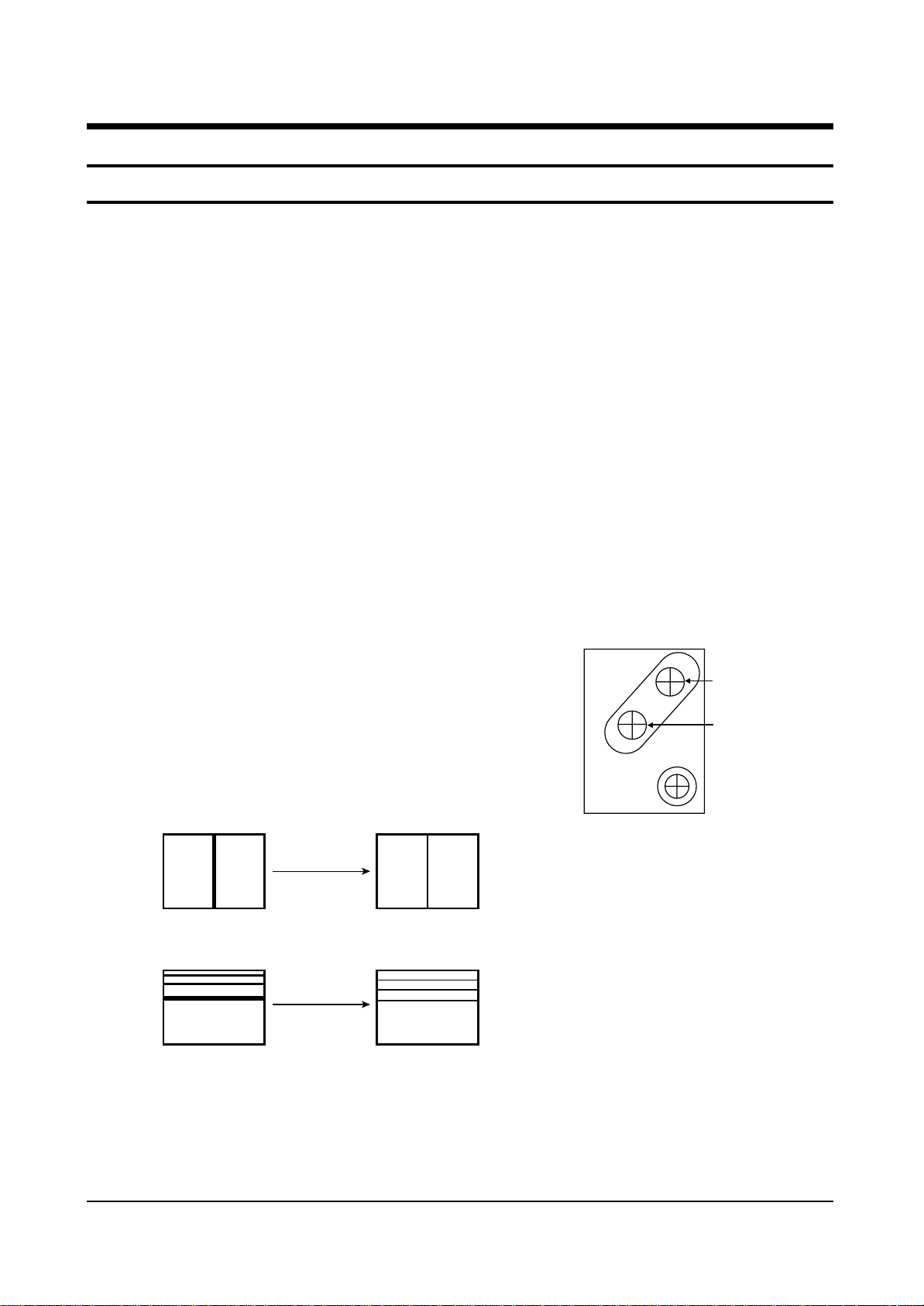
4. Leakage Current Hot Check (Figure 1-1):
Warning: Do not use an isolation
transformer during this test. Use a leakagecurrent tester or a metering system that
complies with American National Standards
Institute (ANIS C101.1, Leakage Current for
Appliances), and Underwriters Laboratories
(UL Publication UL1410, 59.7).
5. With the unit completely reassembled, plug
the AC line cord directly into the power
outlet. With the unit’s AC switch first in the
ON position and then OFF, measure the
current between a known earth ground (metal
water pipe, conduit, etc.) and all exposed
metal parts, including: antennas, handle
brackets, metal cabinets, screwheads and
control shafts. The current measured should
not exceed 0.5 milliamp. Reverse the powerplug prongs in the AC outlet and repeat the
test.
Fig. 1-1 AC Leakage Test
6. Antenna Cold Check:
With the unit’s AC plug disconnected from the
AC source, connect an electrical jumper across
the two AC prongs. Connect one lead of the
ohmmeter to an AC prong. Connect the other
lead to the coaxial connector.
7. X-ray Limits:
The picture tube is especially designed to
prohibit X-ray emissions. To ensure continued
X-ray protection, replace the picture tube only
with one that is the same type as the original.
Carefully reinstall the picture tube shields and
mounting hardware; these also provide X-ray
protection.
8. High Voltage Limits:
High voltage must be measured each time
servicing is done on the B+, horizontal
deflection or high voltage circuits.
Correct operation of the X-ray protection
circuits must be reconfirmed whenever they
are serviced.
(X-ray protection circuits also may be called
“horizontal disable” or “hold-down”.)
Heed the high voltage limits. These include
the X–ray Protection Specifications Label, and
the Product Safety and X-ray Warning Note on
the service data schematic.
Precautions
Samsung Electronics 1-1
LEAKAGE
CURRENT
TESTER
DEVICE
UNDER
TEST
TEST ALL
EXPOSED METAL
SURFACES
2-WIRE CORD
ALSO TEST WITH
PLUG REVERSED
(USING AC ADAPTER
PLUG AS REQUIRED)
EARTH
GROUND
(READING SHOULD
NOT BE ABOVE
0.5mA)
Follow these safety, servicing and ESD precautions to prevent damage and protect against potential
hazards such as electrical shock and X-rays.
1-1 Safety Precautions (Continued)
9. High voltage is maintained within specified
limits by close-tolerance, safety-related
components and adjustments. If the high
voltage exceeds the specified limits, check
each of the special components.
10. Design Alteration Warning:
Never alter or add to the mechanical or
electrical design of this unit. Example: Do not
add auxiliary audio or video connectors. Such
alterations might create a safety hazard. Also,
any design changes or additions will void the
manufacturer’s warranty.
11. Hot Chassis Warning:
Some TV receiver chassis are electrically
connected directly to one conductor of the AC
power cord. If an isolation transformer is not
used, these units may be safely serviced only
if the AC power plug is inserted so that the
chassis is connected to the ground side of the
AC source.
To confirm that the AC power plug is inserted
correctly, do the following: Using an AC
voltmeter, measure the voltage between the
chassis and a known earth ground. If the
reading is greater than 1.0V, remove the AC
power plug, reverse its polarity and reinsert.
Re-measure the voltage between the chassis
and ground.
12. Some TV chassis are designed to operate with
85 volts AC between chassis and ground,
regardless of the AC plug polarity. These units
can be safely serviced only if an isolation
transformer inserted between the receiver and
the power source.
13. Some TV chassis have a secondary ground
system in addition to the main chassis ground.
This secondary ground system is not
isolated from the AC power line. The two
ground systems are electrically separated by
insulating material that must not be defeated
or altered.
14. Components, parts and wiring that appear to
have overheated or that are otherwise
damaged should be replaced with parts that
meet the original specifications. Always
determine the cause of damage or
overheating, and correct any potential
hazards.
15. Observe the original lead dress, especially
near the following areas: Antenna wiring,
sharp edges, and especially the AC and high
voltage power supplies. Always inspect for
pinched, out-of-place, or frayed wiring. Do
not change the spacing between components
and the printed circuit board. Check the AC
power cord for damage. Make sure that leads
and components do not touch thermally hot
parts.
16. Picture Tube Implosion Warning:
The picture tube in this receiver employs
“integral implosion” protection. To ensure
continued implosion protection, make sure
that the replacement picture tube is the same
as the original.
17. Do not remove, install or handle the picture
tube without first putting on shatterproof
goggles equipped with side shields. Never
handle the picture tube by its neck. Some
“in-line” picture tubes are equipped with a
permanently attached deflection yoke; do not
try to remove such “permanently attached”
yokes from the picture tube.
18. Product Safety Notice:
Some electrical and mechanical parts have
special safety-related characteristics which
might not be obvious from visual inspection.
These safety features and the protection they
give might be lost if the replacement
component differs from the original—even if
the replacement is rated for higher voltage,
wattage, etc.
Components that are critical for safety are
indicated in the circuit diagram by shading,
( ) or ( ).
Use replacement components that have the
same ratings, especially for flame resistance
and dielectric strength specifications.
A replacement part that does not have the
same safety characteristics as the original
might create shock, fire or other hazards.
Precautions
1-2 Samsung Electronics

1-2 Servicing Precautions
1. Servicing precautions are printed on the
cabinet. Follow them.
2. Always unplug the unit’s AC power cord from
the AC power source before attempting to:
(a) Remove or reinstall any component or
assembly, (b) Disconnect an electrical plug or
connector, (c) Connect a test component in
parallel with an electrolytic capacitor.
3. Some components are raised above the printed
circuit board for safety. An insulation tube or
tape is sometimes used. The internal wiring is
sometimes clamped to prevent contact with
thermally hot components. Reinstall all such
elements to their original position.
4. After servicing, always check that the screws,
components and wiring have been correctly
reinstalled. Make sure that the portion around
the serviced part has not been damaged.
5. Check the insulation between the blades of the
AC plug and accessible conductive parts
(examples: metal panels, input terminals and
earphone jacks).
6. Insulation Checking Procedure: Disconnect the
power cord from the AC source and turn the
power switch ON. Connect an insulation
resistance meter (500V) to the blades of the AC
plug.
The insulation resistance between each blade
of the AC plug and accessible conductive parts
(see above) should be greater than 1 megohm.
7. Never defeat any of the B+ voltage interlocks.
Do not apply AC power to the unit (or any of
its assemblies) unless all solid-state heat sinks
are correctly installed.
8. Always connect a test instrument’s ground
lead to the instrument chassis ground before
connecting the positive lead; always remove
the instrument’s ground lead last.
Precautions
Samsung Electronics 1-3
Warning1: First read the “Safety Precautions” section of this manual. If some unforeseen circumstance creates a conflict between
the servicing and safety precautions, always follow the safety precautions.
Warning2: An electrolytic capacitor installed with the wrong polarity might explode.

1. Some semiconductor (“solid state”) devices
are easily damaged by static electricity. Such
components are called Electrostatically
Sensitive Devices (ESDs); examples include
integrated circuits and some field-effect
transistors. The following techniques will
reduce the occurrence of component damage
caused by static electricity.
2. Immediately before handling any semicon
ductor components or assemblies, drain the
electrostatic charge from your body by
touching a known earth ground. Alternatively,
wear a discharging wrist-strap device. (Be
sure to remove it prior to applying power—
this is an electric shock precaution.)
3. After removing an ESD-equipped assembly,
place it on a conductive surface such as
aluminum foil to prevent accumulation of
electrostatic charge.
4. Do not use freon-propelled chemicals. These
can generate electrical charges that damage
ESDs.
5. Use only a grounded-tip soldering iron when
soldering or unsoldering ESDs.
6. Use only an anti-static solder removal device.
Many solder removal devices are not rated as
“anti-static”; these can accumulate sufficient
electrical charge to damage ESDs.
7. Do not remove a replacement ESD from its
protective package until you are ready to
install it. Most replacement ESDs are
packaged with leads that are electrically
shorted together by conductive foam,
aluminum foil or other conductive materials.
8. Immediately before removing the protective
material from the leads of a replacement ESD,
touch the protective material to the chassis or
circuit assembly into which the device will be
installed.
9. Minimize body motions when handling
unpackaged replacement ESDs. Motions such
as brushing clothes together, or lifting a foot
from a carpeted floor can generate enough
static electricity to damage an ESD.
Precautions
1-4 Samsung Electronics
1-3 Precautions for Electrostatically Sensitive Devices (ESDs)
Reference Information
Samsung Electronics 2-1
2. Reference Information
2-1 Tables of Abbreviations and Acronyms
A
Ah
Å
dB
dBm
°C
°F
°K
F
G
GHz
g
H
Hz
h
ips
kWh
kg
kHz
kΩ
km
km/h
kV
kVA
kW
I
MHz
Ampere
Ampere-hour
Angstrom
Decibel
Decibel Referenced to One
Milliwatt
Degree Celsius
Degree Fahrenheit
degree Kelvin
Farad
Gauss
Gigahertz
Gram
Henry
Hertz
Hour
Inches Per Second
Kilowatt-hour
Kilogram
Kilohertz
Kilohm
Kilometer
Kilometer Per Hour
Kilovolt
Kilovolt-ampere
Kilowatt
Liter
Megahertz
MV
MW
MΩ
m
µA
µF
µH
µm
µs
µW
mA
mg
mH
mI
mm
ms
mV
nF
Ω
pF
Ib
rpm
rps
s
V
VA
W
Wh
Megavolt
Megawatt
Megohm
Meter
Microampere
Microfarad
Microhenry
Micrometer
Microsecond
Microwatt
Milliampere
Milligram
Millihenry
Milliliter
Millimeter
Millisecond
Millivolt
Nanofarad
Ohm
Picofarad
Pound
Revolutions Per Minute
Revolutions Per Second
Second (Time)
Volt
Volt-ampere
Watt
Watt-hour
Table 2-1 Abbreviations
Reference Information
2-2 Samsung Electronics
Table 2-2 Table of Acronyms
ABL
AC
ACC
AF
AFC
AFT
AGC
AM
ANSI
APC
APC
A/V
AVC
BAL
BPF
B-Y
CATV
CB
CCD
CCTV
Ch
CRT
CW
DC
DVM
EIA
ESD
ESD
FBP
FBT
FF
FM
FS
GND
G-Y
H
HF
HI-FI
IC
IC
IF
Automatic Brightness Limiter
Alternating Current
Automatic Chroma Control
Audio Frequency
Automatic Frequency Control
Automatic Fine Tuning
Automatic Gain Control
Amplitude Modulation
American National Standards Institute
Automatic Phase Control
Automatic Picture Control
Audio-Video
Automatic Volume Control
Balance
Bandpass Filter
Blue-Y
Community Antenna Television (Cable TV)
Citizens Band
Charge Coupled Device
Closed Circuit Television
Channel
Cathode Ray Tube
Continuous Wave
Direct Current
Digital Volt Meter
Electronics Industries Association
Electrostatic Discharge
Electrostatically Sensitive Device
Feedback Pulse
Flyback Transformer
Flip-Flop
Frequency Modulation
Fail Safe
Ground
Green-Y
High
High-Frequency
High Fidelity
Inductance-Capacitance
Integrated Circuit
Intermediate Frequency
I/O
L
L
LED
LF
MOSFET
MTS
NAB
NEC
NTSC
OSD
PCB
PLL
PWM
QIF
R
RC
RF
R-Y
SAP
SAW
SIF
SMPS
S/N
SW
TP
TTL
TV
UHF
UL
UV
VCD
VCO
VCXO
VHF
VIF
VR
VTR
VTVM
TR
Input/output
Left
Low
Light Emitting Diode
Low Frequency
Metal-Oxide-Semiconductor-Field-Effect-Tr
Multi-channel Television Sound
National Association of Broadcasters
National Electric Code
National Television Systems Committee
On Screen Display
Printed Circuit Board
Phase-Locked Loop
Pulse Width Modulation
Quadrature Intermediate Frequency
Right
Resistor & Capacitor
Radio Frequency
Red-Y
Second Audio Program
Surface Acoustic Wave(Filter)
Sound Intermediate Frequency
Switching Mode Power Supply
Signal/Noise
Switch
Test Point
Transistor Transistor Logic
Television
Ultra High Frequency
Underwriters Laboratories
Ultraviolet
Variable-Capacitance Diode
Voltage Controlled Oscillator
Voltage Controlled Crystal Oscillator
Very High Frequency
Video Intermediate Frequency
Variable Resistor
Video Tape Recorder
Vacuum Tube Voltmeter
Transistor

Reference Information
Samsung Electronics 2-3
2-2 Explanation of Landing Compensation Circuit
Landing in the display media using CRT means operation that beam occurred at the electronic gun passes
through a constant hole and arrives to the light emitting object. The more accurate this is, the more even
unified brightness of the whole of screen is uniform. However, landing becomes loose since there is deviation of manufacturing process in the CRT itself and various inside/outside factors.
- Effect of earth magnetic field
There is a magnetic line of force proceeding from South to North in the earth, called as earth magnetic field.
CRT emits light by electron from an electronic gun and direction of this electron becomes reverse direction
of current. Force (F) applies to electron moved by current (I) of the earth magnetic field and the CPT.
Electronic beam fails to arrive a proper position due to this force, which must constantly arrive at the fixed
position of a shadow mask.
2-2-1 Definition
- Effect of ambient temperature
Beam flying to a constant position fails to arrive to the light emitting object by distortion of a mask since
thermal expansion shrinkage of the shadow mask made of metal is different from the side where the light
emitting object is attached depending on temperature.
- Effect of operation time and beam force
Immediately after TV turns on, temperature inside of the CRT rapidly increases by electronic beam and
thereby thermal expansion proceeds in the shadow mask. This proceeds for about 2 hours and accordingly
landing varies. Such a level of change differs depending on the strength of beam shone on the screen
together with time. The stronger strength of the beam is, namely the brighter the screen is, the severer
change of landing is.
The CRT used in the ZEUS is OMEGA CRT of a complete flat32” HD-class with an injection degree of maximum 120’ independently developed and produced by the SDI. It was manufactured in the most minimum
width in the world in comparison with the same size to reduce depth of the set.
Such configuration gives a bad effect on the landing surface and thus landing at the 4 point within the CRT
becomes distorted even by a small ambient effect and purity error (change of color purity: other color)
occurs.
Reference Information
2-4 Samsung Electronics
The following tables show direction of Landing distortion for factors effecting on Landing.
2-2-2 Principle of Operation
The earth magnetic field sensor and the temperature sensor are attached for measuring direction and
strength of the current earth magnetic field and temperature of set. Since effect on the above table must be
compensated, force in the reverse direction must be made.
The following figure shows that coil for landing compensation and coil for TILT compensation are attached
on the rear side of CRT to compensate for it. 4 round coils (coil for landing compensation) is used to compensate for error in the corner where landing error mostly occurs. The TILT coil adjusts degree of the
whole of screen.
** The above tables show direction of actual effect and a reverse direction of it for Landing Data
(direction of microscope). **
Compensation is currently not done for TIME and beam in the landing compensation circuit and circuit
improved in the following version will operate
CRT Direction
Direction of
distorted
landing
EARTH WEST SOUTH NORTH
CRT Direction
Direction of
distorted
landing
Low Temperature High Temperature
TILT COMPENSATION COIL
LANDING
COMPENSATION COIL
COIL VIEWED BEHIND CRT

Reference Information
Samsung Electronics 2-5
- Explanation of Operation
Operation of the landing compensation circuit is controlled by a sub-micom within module. Operation of
the sub-micom for the actual landing compensation is perceived and controlled. It receives values of the
earth magnetic field sensor (SEN01) and temperature sensor (DM01) via the A/D port of the sub-micom
and then perceives the current status and outputs compensation value in the PWM form. Direct driving of
the landing compensation coil is done at the LA6510 power drive OP AMP. Standard operation voltage of
the AMP is made by divided voltage of R028, R029 and applied to the (+) 1N of the OP AMP. The PWM
type of control data that is output from the MICOM is smoothed by the RC integrated circuit and becomes
analog voltage with a constant level. It is applied to the reverse amplitude circuit composed of a power
drive OP AMP via a TR and resistance. In this case, amplitude level is determined by the whole output
impedance and feedback resistance of circuits connected to the (-) 1N terminal of the OP AMP. The LA6510
VSENSE PORT is used for limiting current and can limit the max current value using resistance value
between VOUT terminals. The output flows through the LC coil and creates magnetic field. Position of
electronic beam is compensated by the magnetic field. DC R (voltage at both ends of the LC coil measured
by DVM as direct current resistance component) of the LC coil is about 100 ohm.
Details of explanation are deleted since operation of the tilt coil operates even in general TV.
- Inspection of Operation
Operation inspection after set repair is as follows:
1) Is the output terminal (red, gray, blue, black) of coil at the aging mode within 9 +/- 300mV?
2) Does other color occur when removing the PCB Front Connector(CN905A) from the Main Chassis?
3) Does other color occur when touching magnetic object near the earth magnetic field Sensor Module?
Where all answers for the above questions are Yes, they show that the Landing compensation circuit
properly operates for the set.
2-2-3 Operation of Circuit
Two matters are related each other in the factory mode.
Factory mode -> TL, BL, TR and BR value are value of the area that user (service man) can vary.
It is better not use these values unless purity error occurs (where, TL, BL, TR, BR represents TOP LEFT,
BOTTOM LEFT, TOP RIGHT and BOTTOM LIGHT, respectively).
Factory mode -> There are TL, BL, TR, BR and SENCE LRR types in the ITC. They must not be changed.
There is information about CRT and the circuit part for compensating it. However, in replacing EEPROM
or main chassis, change of it is needed but the value of sense REF must not be changed.
(The sense REF is used to compensate for sensor unique omission and is line adjustment value that reads
center value of sensor in the 0-earth magnetic field and stores it at the EEPROM. Since the 0-earth magnetic
field cannot be made in the field, this item shall not be changed. If changing it and thus purity error occurs,
the EEPROM must be replaced according to the following cautions)
2-2-4. Related OSD Matters

Reference Information
2-6 Samsung Electronics
Check item prior to repair
1) Is the +- output terminal (Red, Gray, Blue, Black) of a coil in the Aging Mode within 0 +/- 300mV?
2) Does other color occur when removing the PCB front connector from the main chassis?
3) Does other color occur when touching approaching magnetic object around the earth magnetic field
Sensor Module?
If all answers for above questions is Yes, it means landing compensation circuits properly operates for the
set.
1) Cautions in replacement of parts and E2PROM in earth magnetic field
You should replace an E2PROM within the main chassis and the main chassis in the following orders if
necessary:
Where set operation is possible
a) Memorize values of TL, BL, TR and BR from the Factory Mode -> TIC. Sense REF values should not be
changed at any case (If pressing + - key, current values of the earth magnetic field becomes standard
value and emergent operation is done by it).
b) Replace parts.
c) Change it into TL, BL, TR and BR memorized from the Factory Mode -> TIC. Sense REF values should
not be changed at any case (In this case, initial value is 115, 125).
d) Inspect operation status.
e) If there is no abnormality in the operation inspection but other color occurs, change and adjust
four value(TR, BL, TR, BR) from the Factory Mode ->User so that there is no purity error.
Where set operation is not possible
a) Replace parts.
b) Change should not be done at any case in the Factory Mode -> TIC mode.
(In this case, initial value is 115, 125).
c) Inspect operation status.
d) If there is no abnormality in the operation inspection but other color occurs depending on ambient
conditions, change and adjust 4 values from the Factory Mode ‡User so that there is no purity error.
2-2-5 Cautions in troubleshooting

Reference Information
Samsung Electronics 2-7
2) Cautions in De-Gaussing
1. ADG (Auto Degaussing)
- There is no problem since set itself operates in the Degaussing operation of set itself under the Purity
Off Mode.
However, the set normally operates when performing Power On after Off for 30 minutes after removing
power.
2. HDG (Hand Degaussing)
- If desiring to operate the compulsory Degaussing mode, you should set “Aging Mode” for operation.
3. AGING MODE
- A strong magnetic field occurred in the HDE-GAUSSING affects on sensor in the earth magnetic field
and as a result, a strong magnetic field occurs from the LC coil. It is not good for sense operation and
DE-GAUSSING of the earth magnetic field. Be sure to perform semsing and DE-GAUSSING magnetic
field in Aging Mode, especially whem adjusting user values.
Reference Information
2-8 Samsung Electronics
2-2 IC Line Up
Block Des-Loc Part-Number IC Name Description
MAIN
IC601
IC701
IC702
IC703
TU01
TUP01
IC905
ICH01
IC602
ICD603
IC603
IC804
IC805
IC802
1204-001594
1001-001073
1001-001113
1002-001193
AA40-00020A
AA40-00032A
1103-001171
1204-001454
1201-000407
1201-001385
1201-001385
1203-000203
1203-000203
1203-000293
MSP3440G-B6
TEA6415C
TEA6422
PCF8591P
TCLN318PA09A(S)
TCPN3081PC09A(S)
24L161
TDA7449L
TDA7050
TDA7269A
TDA7269A
SI3050
SI3050
KA7808
IC-SOUND PROCESSOR
IC-VIDEO SWITCH
IC-AUDIO SWITCH
IC-A/D & D/A CONVERTER
TUNER-F/S
TUNER-F/S
IC-EEPROM
IC-VOLUME CONTROL
IC-POWER AMP
IC-POWER AMP
IC-POWER AMP
IC-POSI.ADJUST REG.
IC-POSI.ADJUST REG.
IC-POSI.FIXED REG.
POWER
IC803
IC801
IC301
D801S
IC801S
IC803S
Q403
Q404
QH407
QH408
QH406
1203-000298
1203-000165
1204-000517
0402-001399
1203-002091
AA13-00024A
0505-000156
0505-001116
0502-001187
0502-001104
0502-001100
KA7809
78R12
LA7845
GSDIB660
STR-F6658B
TNY253P
IRF620
BUZ73A
2SC5612
2SD921
2SD4125
IC-POSI.FIXED REG.
IC-POSI.ADJUST REG.
IC-VERTIVAL DEF.
IC-HYBRID
IC-HYBRID
IC-HYBRID
FET-SILICON
FET-SILICON
TR-POWER
TR-POWER
TR-POWER

Reference Information
Samsung Electronics 2-9
Block Des-Loc Part-Number IC Name Description
QH405
DH401
DH400
Q801
IC01
IC02
IC05
IC06
IC07
IC03
IC04
PIC01
PIC02
PIC04
PIC05
IC902
IC903
IC11
IC12
IC13
IC14
IC04
IC501
IC502
IC503
QF10
QF09
IC504
0505-001202
0402-001176
0402-001176
1004-000101
1204-001598
AA13-00095A
1002-001045
1204-001372
1204-001550
1105-001035
1105-001035
1204-001598
1109-001144
1203-001419
1203-001419
1203-001140
1203-001274
1203-001419
1203-001140
1203-001359
1202-000001
1203-001419
1201-001588
1201-001588
1201-001588
0502-000153
0502-000131
1201-000010
IRF640
FMQG5GS
FMQG5GS
SE140N-DIP
VPC3230D-A0
SDP01
SDA9280
SDA9361
CXA2101AQ
416S1120
416S1120
VPC3230D-A0
81V04160
4931
4931
7039
7545
4931
7039
1086
KA7533
4931
TDA6120Q
TDA6120Q
TDA6120Q
2SC2344-D
2SA1011A-D
2030
FET-HYBRID
TR-DIODE
TR-DIODE
IC-HYBRID
IC-VIDEO PROCESS
IC-ASIC
IC-D/A CONVERTER
IC-HOR./VER.PROCESS
IC-VIDEO PROCESS
IIC-DRAM
IC-DRAM
IC-VIDEO PROCESS
IC-FIFO
IC-VOLTAGE REGULATOR
IC-VOLTAGE REGULATOR
IC-VOL.DETECTOR
IC-VOL.DETECTOR
IC-VOLTAGE REGULATOR
IC-VOL.DETECTOR
IC-POSI.FIXED REG.
IC-VOLTAGE COMP.
IC-VOLTAGE REGULATOR
IC-VIDEO AMP
IC-VIDEO AMP
IC-VIDEO AMP
TR-POWER
TR-POWER
IC-OP AMP
POWER
F-BOX
CRT
Reference Information
2-10 Samsung Electronics
Block Des-Loc Part-Number IC Name Description
IC901
IC01
IC005
IC006
IC001
IC003
SEN01
DM03
IC601
IC602
AA13-00101A
1204-001556
1201-001199
1201-001199
1203-000515
AA09-00070A
AA32-00010A
1404-001039
1204-0001198
1201-000541
Z9037116PSC-OTP
UPD64082GF
IC-POWER AMP
IC-POWER AMP
IC-VOL. DETECTOR
IC MCU
SENSOR MAG
THERMISTOR-NTC
IC-DECODER
IC-OP AMP
IC-MCU
IC-SEPARATOR
6510, SIP
6510, SIP
7042, T0-92, 3P
SPR2000, 42P
TMC3000NF, 35MA
Kohm, 1%, 3435K
DPL3519A
062
MICOM
3D-COMB
SUB
MICOM
CRT
SENSOR
TACK S/W
DOLBY
Specifications
Samsung Electronics 3-1
3. Specifications
Specifications are subject to change.
Model
Dimensions
(mm)
Weight
Set
Transmitter
Tuning Ranges
Television System
Intermediate Frequency
TSL3099WHFX
67 Kg
153 g (including batteries)
Hi Contrast Instant Reception Type
VHF (CH 2 ~ 13)
UHF (CH 14 ~ 69)
CATV (CH 1, 14 ~ 125)
NTSC-M
VHF, UHF: 75 ohm unbalanced type
Video: 45.75 MHz
Sound: 41.25 MHz
Chrominance Subcarrier: 42.17 MHz
Reverse Automatic Gain Control (Reverse AGC)
910 (W) x 455 (D) x 578 (H)
54 (W) x 31.5 (D) x 220 (H)
Set
Transmitter
Picture Tube
Antenna Input
Automatic Gain Control
Power Supply
AC 120 V, 60 Hz
DC 1.5V (AAA Size) x 2
180 W
Insulation Switch
7.5 W x 2, WOOFER : 25W x 1
Transmitter Adjustment: Infrared Rays Type
UHF/VHF electronic tuner fine tuning: Electronic Type
Electronic Function Adjustment
Power Consumption
Rectification
Sound Output
Adjustment System
Set
Transmitter

3-2 Samsung Electronics
MEMO
Alignment and Adjustments
Samsung Electronics 4-1
4. Alignment and Adjustments
4-1 Adjustments
Usually, a color TV needs only slight touch-up adjustment upon installation. Check the basic
characteristics such as vertical size, horizontal size, and focus. Observe the picture and check for
good black and white details. There must be no objectionable color shading: If color shading is
present, demagnetize the receiver. If color shading persists, re-do purity and convergence adjustments.
Note :
1. This ‘4. Alignment and Adjustments’ applies to KS4A chassis applications.
2. AC Power Supply: 220 V only
3. This service manual has been written on the basis of domestic remote-control model adopting KS4A
chassis. Depending on sales location and product specifications, some of specifications herein may
be changed.
KS4A contains a dynamic focus circuit. When CRT PCB, FBT or CRT is replaced, be sure to adjust
in the following sequence:
4-1-1 General Alignment Instructions
4-1-2 Focus Adjustment
Dynamic Focus Adjustment
1. Input a crosshatch pattern.
2. Select “Standard” from the menu,
3. Turn the Static Focus VR clockwise to set it to its maximum.
4. Turn the Dynamic Focus VR counterclockwise to set it to its
maximum.
5. Turn the Static Focus VR counterclockwise slowly for the clearest
center vertical line.
<FBT FOCUS PACK>
6. Turn the Dynamic Focus VR clockwise slowly for the clearest third line.
7. Check for the FOCUS of entire screen. If necessary, re-do adjustments 3~6.
V
STATIC FOCUS VR
H
DYNAMIC FOCUS VR
NO USE
After Adjustment
1
2
3

Alignment and Adjustments
4-2 Samsung Electronics
4-1-3 Screen Voltage Adjustment
1. Enter the Video/Component Mode. Just connect a jack and do not supply a video signal.
2. Use a DC multi-meter to identify RK, GK, BK. And then adjust FBT Screen VR so that the highest
voltage becomes 175 Vp-p.
4-1-4 White Balance Adjustment
1. Select “Standard” from the menu.
2. Input an 100% White pattern.
3. In standby, press the remote-control keys in the following sequence: Mute 1 8 2
Power on the TV set.
4. Warm up the TV set at least for 30 minutes.
5. Input a 10-step stair signal.
6. Use the Volume +/- buttons on the remote-control to select RDR, GDR, BDR, CON.
7. Adjust High-Light while viewing the brighter side of screen.
8. Use the Volume +/- buttons on the remote-control to select RCT, GCT, BCT, SBT.
9. Adjust Low-Light while viewing the darker side of screen.
10. If not proper, re-adjust White Balance.
11. Press the Power button to exit.
4-1-5 Sub-Brightness Adjustment
1. In standby, press the remote-control keys in the following sequence: Mute 1 8 2
Power on the TV set.
2. Use the Channel Up/Down buttons to receive the sub bright adjustment signal.
3. Use the Volume +/- buttons to select SBT.
4. Press the Menu or Mute button on the remote control to adjust so that the seventh step on
the right of screen cannot be seen.
5. Press the Memory button to exit.
Alignment and Adjustments
Samsung Electronics 4-3
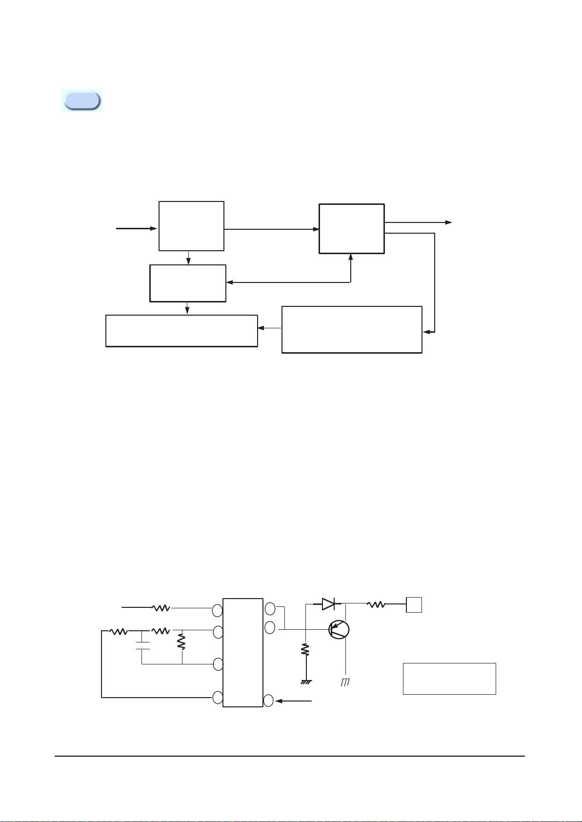
This circuit uses in pulse width modulation method to check high voltage difference
and then adjust energy of storage trans, in order to compensation and stabilize high voltage.
1)Block Diagram
Note1.
HIGH VOLTAGE REGULATOR CIRCUIT (Digital TV) : 32”, 36”
2) Circuit description
This circuit detect high voltage difference from FBT, will be compared with reference voltage of HVIC02.
The varied voltage will be changed pulse width modulation by PWM Generator HV IC02 .
This pulse will vary energy of storage trans(TD402S) according to high voltage difference the varied energy
is added to basic high voltage pulse of FBT. As a result, this circuit will be stable high voltage.
2-1) Working description in case of high voltage Up & Down
In case high voltage goes up(or down) due to change of beam current, the voltage of
high voltage detection prove will be goes up(or down) according to Divider resistance value
(which are inside of FBT(T444) and outside resistance), and this increased voltage will be
supplied to PWM PULSE IC(HVIC02) pin #1.
B+ input
PWM OUT FET(QH405)
(HVQ06 Ic Current control)
HV OUT
Transistor
(QH40 6 )
storage
trans(TD402S)
F.B.T
(T444S)
PWM generator & check
high voltage differe nce
(HVIC02)
High voltage
output
High voltage
Check
high voltage
Detector
HVR19
reference voltage
HVR20
HVR02
HVR14
1
2
3
14
HVIC02
9
10
HVR10
4
HVDZ01
F/S CHECK
HVR36
HVQ01
TS13
PWM PULSE
OUT PUT
ASSY-H/V
MODULE
Alignment and Adjustments
4-4 Samsung Electronics
This IC(HVIC02) provide a complete pulse width modulation system in a single monolithic intergrated
circuit.
The voltage which is inputed to HVIC02 pin #1 will be compared with reference voltage
(HVIC02 pin #14, 5V), and then its difference voltage will be amplified.
Its value will be convert PWM pulse in HVIC02, and then PWM pulse will be output from HVIC02
pin #9,#10. Transistor HVQ01 is used as Buffer for impedance matching.
The PWM duty which is outputed from HVQ01 is variable according to Beam current of high voltage.
In case high voltage goes up (or down) due to change of Beam Current, PWM duty will be decreased
(or increased).
This pulse which is inputed to QH406 Gate(FBT) will be turn on between source and drain,
and IC current of QH405 will be flow to primary of storage trans (TD402S) and then will be charge energy
in primary of storage trans during trace period .
This energy is variable according to pluse duty, and will be inducted to secondary of TD402S.
The inducted energy will be added to basic high voltage generation pulse in FBT (T444S).
As a result, high voltage will be regulated by this method.
3) F/S circuit description
In case high voltage goes up, consequently detected voltage will be goes up and this voltage will be divided
regularly through R432,R433,R434,RR400S R and R441.
H- DRIVE
QH405
TS13
R449
CR410S
QH406
G
DZ400
D
S
R486
L403
CR409S
D410
L481
+B INPUT
C47 2
5
11
TD402S
CR411S
6
9
1
2
FBT
T444S
High
voltage
output
T444S
ANODE
X- ra y T es t pin
R1
¤æ
Hight voltage
check voltage
C48 0
R4 31
R4 30
RR401S
R432
HVR20
R433
HVIC02¤ PIN
¤¤
R434
R4 37
TL494CN
HV- REG.
RR400S
R441
D411
R
HVIC03
TL431
F/S

Alignment and Adjustments
Samsung Electronics 4-5
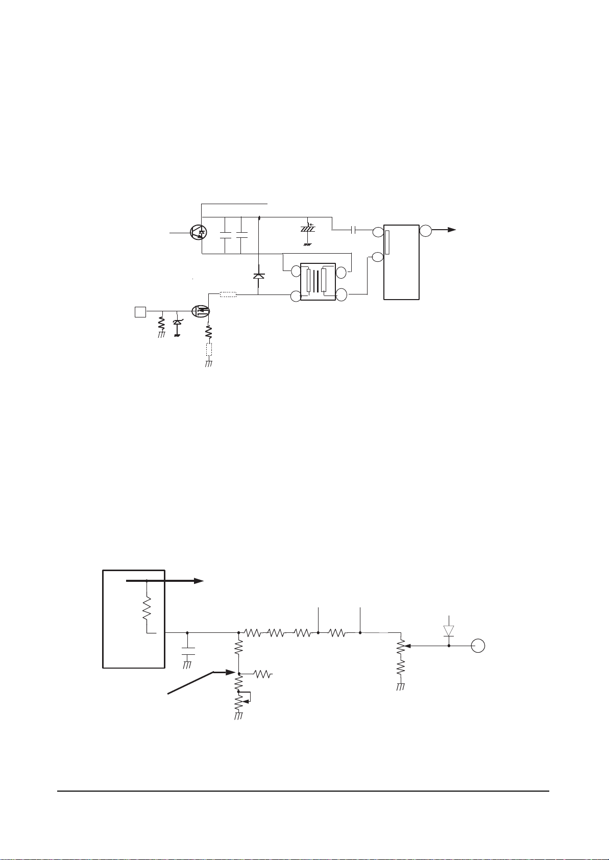
This divided voltage will be inputed to HVIC03 pin #R, and then in this case voltage goes up more than
2.95V, Between pin #K and pin #A of HVIC03 will be turn on and will be decreased
Base voltage of HVQ02, and then E-C of HVQ02 will be turn on and will be detected high level voltage
by R482. Its value will be inputed HVIC02 pin #4(X-ray detect) , and high voltage oscillation will be OFF
in order to protect X-ray.
In this case, high voltage will be On if power is re-ON.
+12V
HVC03
HVR01
HVQ02
HVR13
F/S Detector
R
K
HVC02
HVIC03(TL43 1)
A
HVR25
HVR08
HVD01
TS14
HVDZ02
4
HVIC02
X- ray

Alignment and Adjustments
4-6 Samsung Electronics
The high voltage hold-down circuit prevent TV from damage caused by abnormal high voltage.
The high voltage hold-down circuit is implemented by detecting the variation of Heater voltage because
heater voltage varies with the variation of high voltage.
When the input voltage (A-Point) of QX01’s RESET IC is higher than 4.5V, MICOM #3 port is turned to
“HIGH” then power-off follows.
So to speak, if MICOM #3 port becomes “HIGH”, MICOM #1 port is controlled (from “HIGH” to “ LOW”)
and power-off is implememted.
Note2.
HOLD-DOWN OR SAFETY CIRCUIT INFORMATION : 29”, 34”
Fail Safe Test Point

Alignment and Adjustments
Samsung Electronics 4-7
4-2 SZM 414AZ (ZILOG90371) Micom
4-2-1 Pin Layout
 Loading...