

Page 1

‘ 01 SHORT COURSE =====
(S-2)
Fundamentals of Active -Matrix
Liquid-Crystal Displays
(Sunday, June 3, 2001)
Sang Soo Kim, Ph.D.
Vice President, AMLCD Div.
Semiconductor Business
Samsung Electronics Co., Ltd.
Kyunggi-Do, Korea
Page 2

Fundamentals of Active -Matrix
Liquid-Crystal Displays
I. Introduction
II. Liquid Crystal Displays
III. Structure of Color TFT -LCDs
IV. Basic Operation Principles &
Design of Color TFT-LCDs
V. Color TFT-LCD Fabrication Process
VI. Summary and Projections
Page 3
I. Introduction
• What is Liquid Crystal ?
• Structure of L/C
• Alignment of L/C
• TN & STN Modes
• Normally White and Black Modes
Page 4
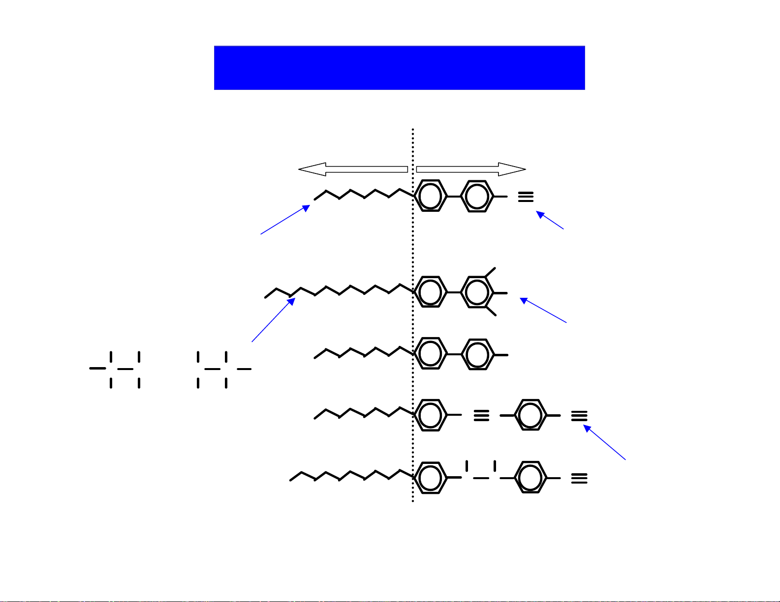
What is Liquid Crystal ?
Flexible Part Rigid Part
C
N
H
Terminal Group
H H
C C
H H
Alkyl Chain
...
H H
C C
H H
Alkyl group Biphenyl group Terminal Group
F
F
F
F
C C
H N
C C C
Fluorine
C
N
N
Cyano Group
Figure 1. The structure of a L/C
Page 5
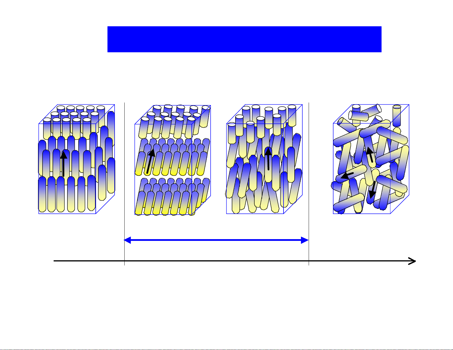
Phases of L/C vs. Temperature
* Operating Temperature Range for Display Application
Solid
Crystalline
(Melting Point)
Smectic Phase Nematic Phase
Liquid Crystalline
Tm
(Clearing Point)
Figure 2. Phases of a Liquid Crystal
Tc
Liquid
Isotrope
Temperature
Page 6
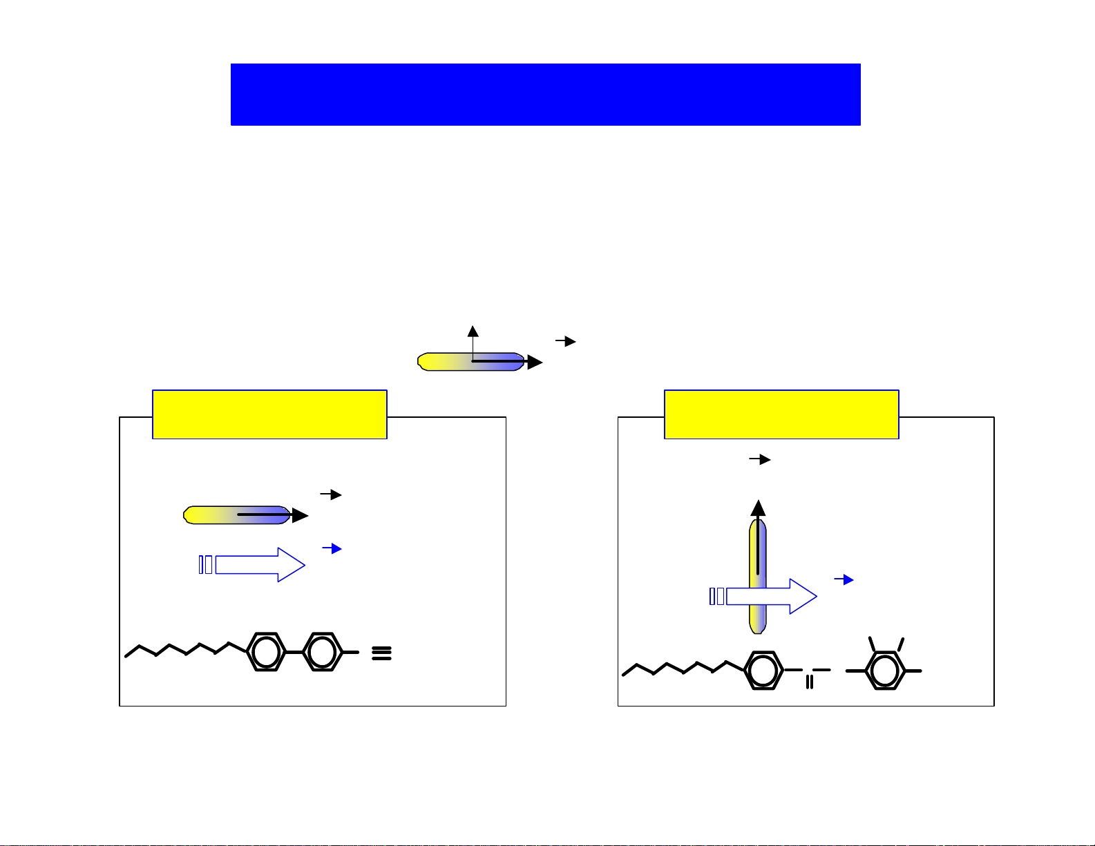
Structure of Liquid Crystal
Birefringence: ∆n = -n
e
n
o
Dielectric Anisotropy: ∆ε = -εe εo
n
o
εo
n
e
εe
D(Director)
p-type (∆ n >0) n-type (∆ n <0)
ne > no ne < no
D
D
E
C
N
Figure 3. Anisotropy of a L/C
E
C O
O
F
F
OC2H
5
Page 7
Intermolecular Attraction: Long Axis > Short Axis
n
n
n
n
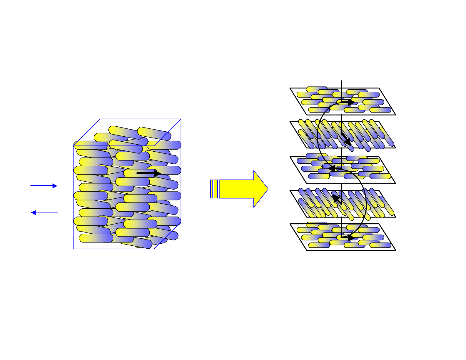
move
Nematic
Figure 4. Types of liquid crystal phases
n
Chiral Dopant
n
Cholesteric
Page 8
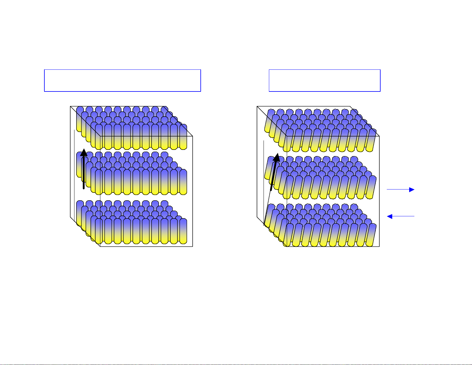
Intermolecular Attraction: Short Axis > Long Axis
Perpendicular to the layer
n
Tilted to the layer
n
move
Smetic A
(SmA)
Figure 5. Types of Liquid Crystal Phases
Smetic C
(SmC)
Page 9
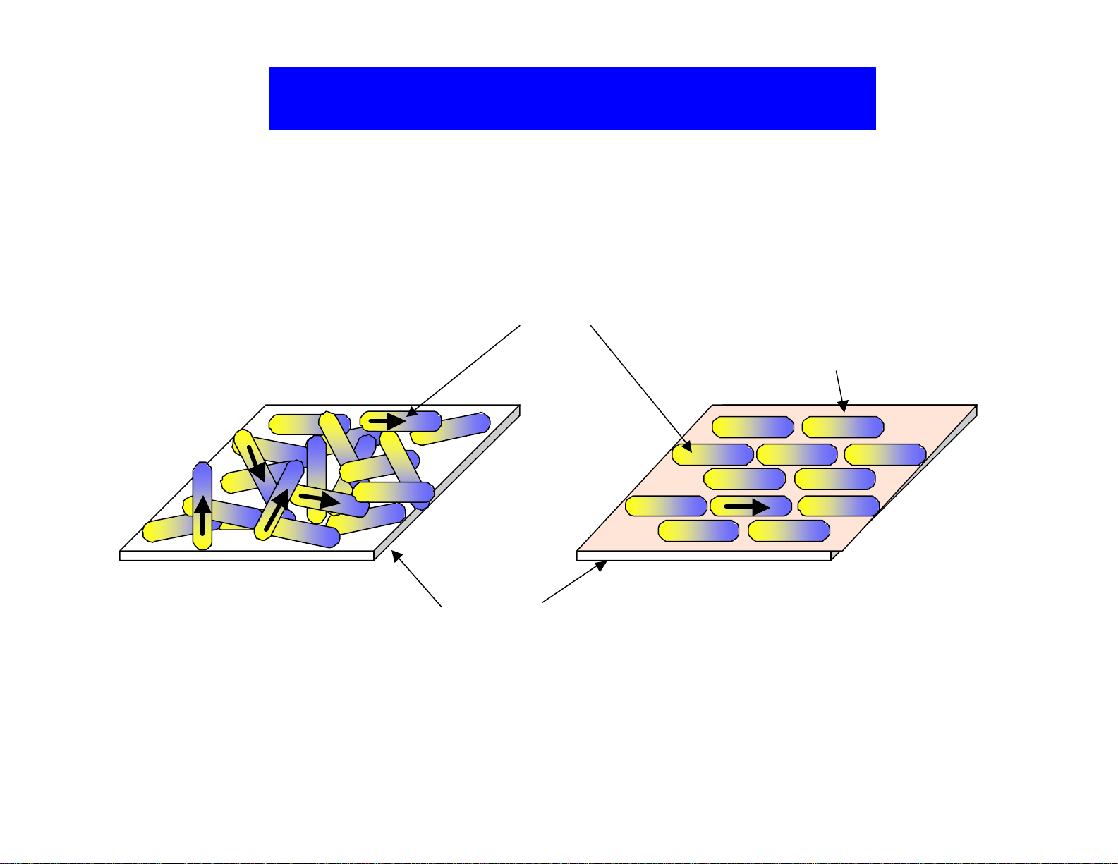
Alignment of Liquid Crystal
Interaction: L/C Molecule & Substrate
L/C Molecule
Alignment Layer
Glass Substrate
Figure 6. Liquid crystal alignment layer
Page 10
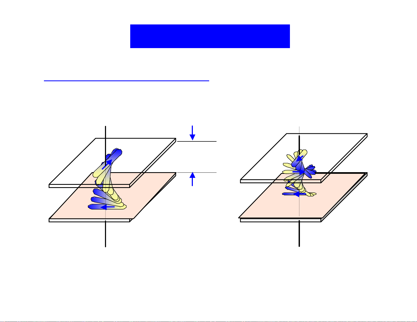
TN and STN Modes
Mauguin’s Condition for TN: ∆n? p = ∆ n? d x 2π/Θ > λ
Retardation for TN: ∆ n? d = 0.3~0.5µm
D~ 5µm
Φ = 90°
TN Mode
180°< Φ < 270°
STN Mode
Figure 7. Orientation of L/C molecules in TN and STN cells
Page 11
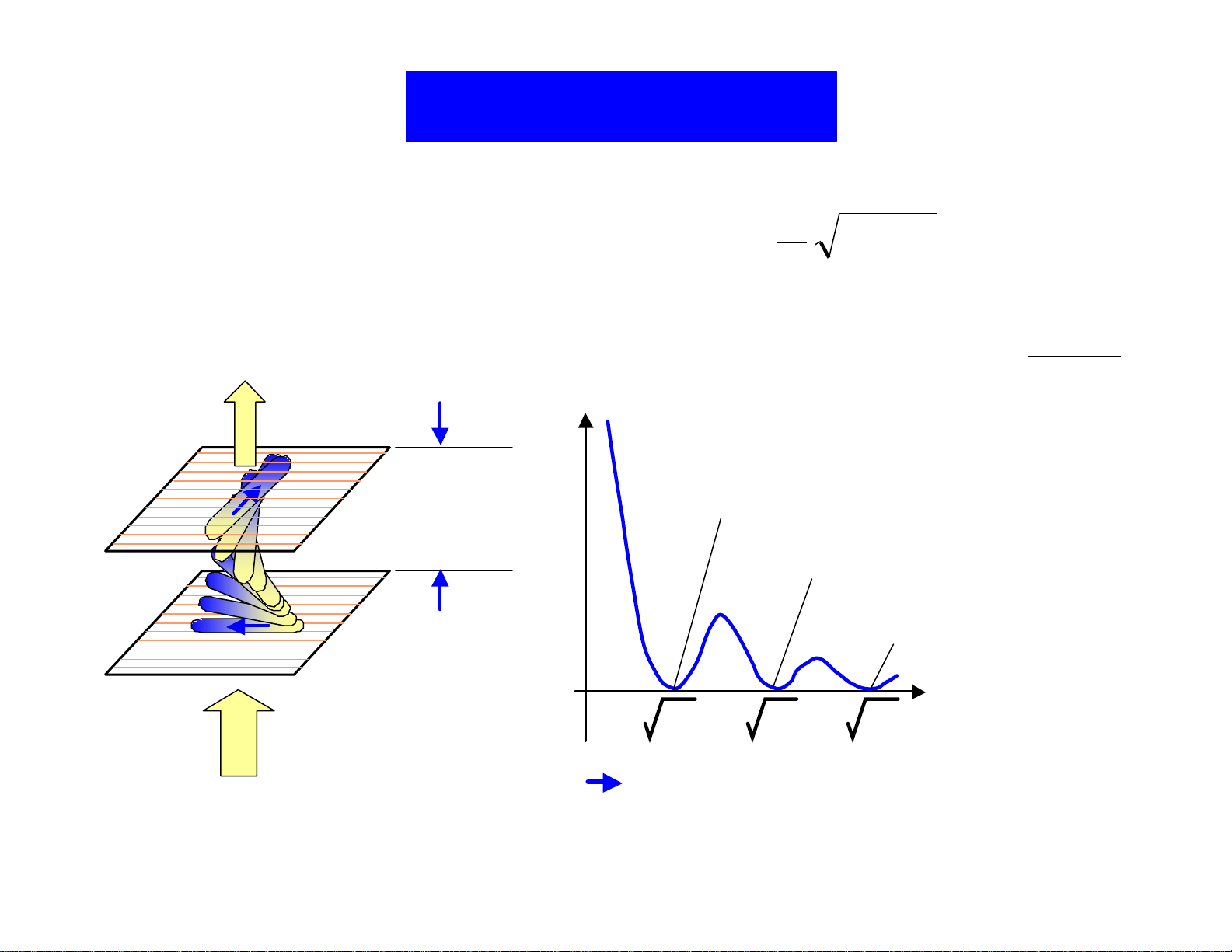
2
/
Design of TN Cell
Gooch -Tarry’s Law:
Normal Black Mode
(1st min.)
d~ 5µm
T = sin
T
π
2 2 2
1 1
2
u u
+
/
( )
+
∆
w u =
ith
λ
1st Minimum (∆n d ~ 0.48µm)
2nd Minimum (∆n d ~ 1.47µm)
3rd minimum
n d
⋅
u
3 15 35
∆n=0.09~0.10 5µm 14.7µm
Figure 8. Design of TN cell
Page 12

NW-Mode
V-T Characteristics
Transmittance(%)
100
90% Trans.
STN
50
TN
TN-Mode
(V10/V
~ 1.6)
90
Vth
STN-Mode
(V10/V
Figure 9. V-T curves for TN and STN cells in NW mode
~ 1.06)
90
0
1.0 2.0 3.0 4.00
L/C Voltage (V)
Vsat
10% Trans.
Page 13
NW Mode TN Cell
Normal White (NW) Mode:
• Higher C/R, True Black
• Less Cell Gap Dependent
Cross Nicols
Optical
Rotation
Light On
0 volt 5 volt
Polarizer(2)
L/C
Polarizer(1)
E
Light Off
No
Optical
Rotation
BacklightBacklight
Figure 10. Normally white mode TN cell
Page 14
NB Mode TN Cell
Light Off
0 volt 5 volt
Light On
Polarizer(2)
L/C
E
Polarizer(1)
BacklightBacklight
Figure 11. Normally black mode TN cell
Page 15
II. Liquid Crystal Displays
• Passive and Active Matrix LCD’s
• Kinds of AMLCD’s
Page 16

Liquid Crystal Operating Modes
• TN (Twisted Nematic)
• STN(Super TN)
• DSTN(Double STN)
• FLC(Ferroelectric LC)
• GH(Guest-Host)
• DS(Dynamic Scattering)
• PDLC(Polymer Dispersed LC)
• VA(Vertical Alignment)
• IPS(In-plane Switching)
Page 17
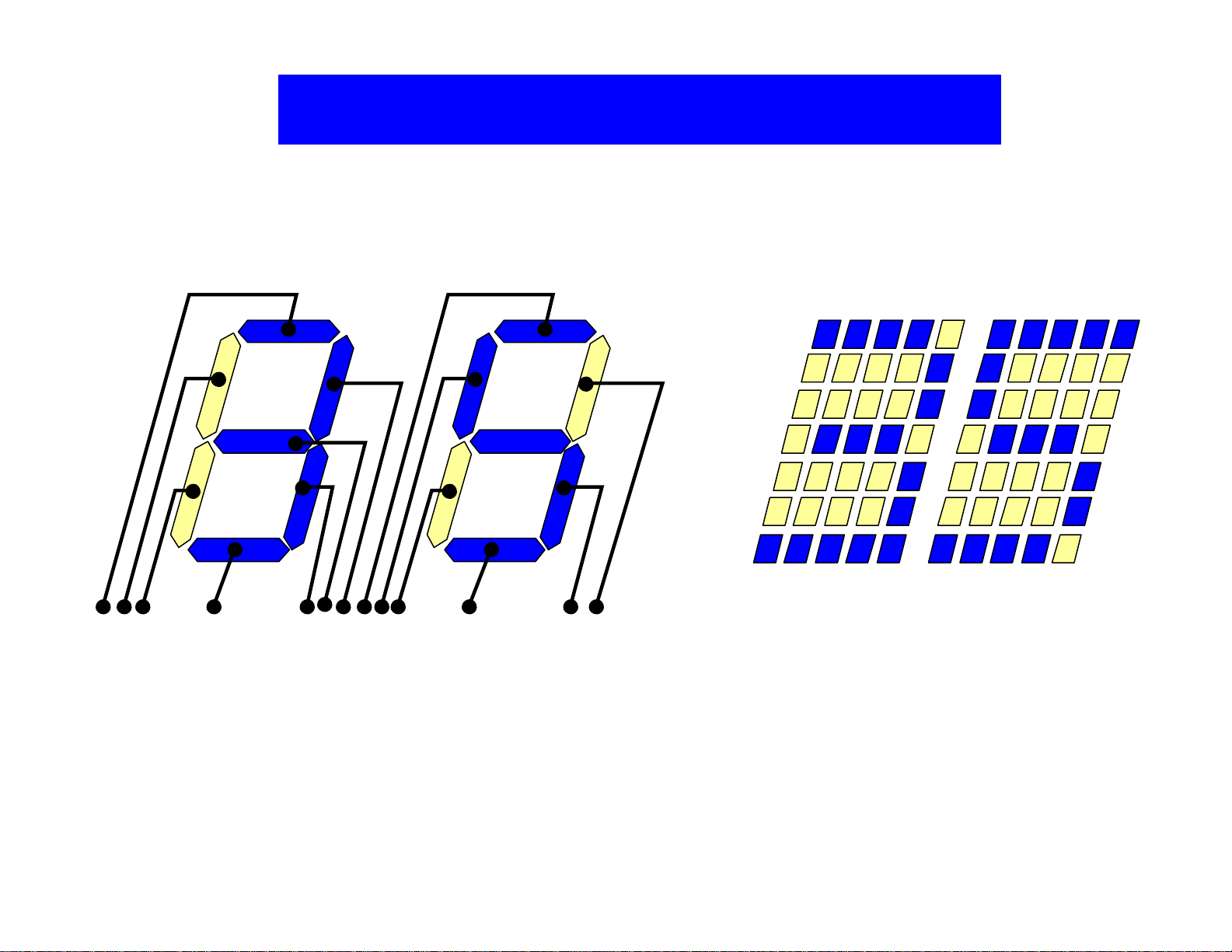
Segment & Dot- Matrix Driving
Segment Display
(7-segment)
Figure 12. Example of rendering an L/C image using direct driving
Dot-Matrix Display
(5x7 matrix)
Page 18

Multiplex Driving of Dot- Matrix Display
Signal Electrodes
Scanning
Electrodes
x1 x2 x3 x4 x5 x6
y1
y2
y3
y4
y5
y6
y7
x1 x2 x3 x4 x5 x6
y1
y2
y3
y4
y5
y6
y7
Figure 13. Example of rendering an L/C image by multiplex drivin g
Page 19

Application of LCDs
• Projection Type: LCD Projector, OHP, Projection TV
• Direct View Type: Notebook PC, LCD Monitor, Potable TV, ViewCam
• Reflective Type: PDA, Cellular Phone, Game
• Transflective Type : PDA, etc.
Page 20

LCD Projector (3-Panel System)
Dichroic
Mirror
LCD(1)
Mirror
Blue Red Green
LCD(2)
Projection
Lens
Screen
I I I
R G B
Mirror
Dichroic
Mirror
Figure 14. LCD Projector using three black and white LCD’s
LCD(3)
Composed
3I
Color Image
Page 21

LCD Projection TV (Single-Panel System)
Mirror
Screen
B(I/3)
G(I/3)
R (I/3)
Spatially divided
Color Image
Mirror
Figure 15. LCD projection TV using a color LCD
Lamp
Lens System
LCD Panel
(Color)
Mirror
Page 22

Color TFT-LCD Module (Direct View)
Backlight Lamp
LCD Panel
Reflector
LGP
Figure 16. An example of direct view LCD’s
Diffuser
BEF
LDI Chip
Chassis Unit
Page 23

Kinds of AMLCD’s
Passive Matrix LCD (PMLCD)
Active Matrix LCD (AMLCD)
MIM-LCD
Diode-LCD
TFT-LCD
a-Si TFT-LCD
poly Si-LCD
Low Tem. poly-Si LCD
High Tem. poly-Si LCD
Page 24

III. Structure of Color TFT-LCD
• Color TFT-LCD Panel
• Driving Circuit Unit
• Backlight and Assembly Unit
Page 25

Structure of Color TFT-LCD
? LCD Panel
? Driving Circuit Unit
TCP
PCB
Chassis
LDI
Lamp
Color Filter
Substrate
TFT-Array
Substrate
LGP
? LCD Panel
? TFT-Array Substrate
? Color Filter Substrate
? Driving Circuit Unit
? LCD Driver IC (LDI) Chips
? Multi-layer PCBs
? Driving Circuits
? Backlight & Chassis Unit
? Backlight Unit
? Backlight & Chassis
Unit
Figure 17. Structure of a color TFT-LCD module
? Chassis Assembly
Page 26

Structure of Color TFT-Panel
Common Electrode
Black Matrix
Seal
Short
TFT-Array Substrate
Bonding PAD
(ITO)
Color Filter Substrate
TFT
Pixel Electrode
(ITO)
L/C
Spacer
Storage Capacitor
Polarizer
Color-Filter
(Blue)
Alignment
Layer
Polarizer
Figure 18. The vertical structure of a color TFT-panel
Page 27

Structure of Driving Circuit Unit
LCD panel
Gate PCB
LDI Chip
(Gate)
Source PCB
LDI Chip
LCD Control
(Source)
ASIC
Figure 19. Assembly of LCD driving circuits
Interface
Connector
FPC
Connector
Page 28

Types of Backlight Units
Top-down
Reflector
Light
Diffuser
CCFL
(Cold Cathode Fluorescent Lamp)
Edge-light
Light
Reflector
Figure 21. Two different types of LCD backlight systems
LGP
Diffuser
CCFL
Page 29

Types of LCD Module Package
Flat TCP
Driving Circuit
Unit
Bent TCP
LGP
Chassis
LCD Panel
Diffuser
Reflector
Chassis Unit
CCFL
Driving Circuit
Unit
Figure 20. Slim type LCD module package
Tapered LGP
(t<2.5mm)
CCFL
(d<2.0mm)
Page 30

Improvement of Backlight Brightness
* BEF: Brightness Enhancement Film
Prism Effect
Prism Sheets
CCFL
Lamp Reflector
Figure 22. Improvement of B/L brightness using BEF
(BEF)
Diffuser
Reflector Sheet
LGP
Page 31

IV. Basic Operation Principles and
Design of Color TFT-LCD
• Operation of TFT-LCD Pixels
• Gray Scale Generation
• Color Generation
Break
• TFT Design
• Storage Capacitor Design
• Signal Bus-Line Design
• Aperture Ratio
• Design for Redundant
Page 32

Structure of Color TFT-Panel
TFT-Array
Substrate
(m x n) Resolution
(3m x n) active matrix
3m (800xRGB)
Bonding Pad
Color-Filter
Substrate
R G B
n
(600)
Unit Dot
(R,G,B sub-pixels)
SVGA: 800 x RGB x 600
(2400 x 600) Matrix
Figure 23. Active matrix structure of a color TFT-panel
Page 33

Resolution of Color LCDs
Resolution # of Dot # of Pixel
Aspect
Remark
Ratio
320 x 240
640 x 400
640 x 480
800 x 480
800 x 600
102 4 x 600
102 4 x 768
1280 x 1024
1400 x 1050
1600 x 1200
1920 x 1200
2048 x 1536
76,8 00 230,4 00 4:3 Quarter VGA
256,000 768,0 00 16:1 0 EGA
307,200 921,6 00 4:3 VGA
384,000 1,15 2,000 15:9 Wide VGA
480,000 1,44 0,000 4:3 SVGA
614,400 1,84 3,200 ~17:10 Wide SVGA
786,432 2,35 9,296 4:3 XGA
1,3 10,720 3,92 3,160 5:4 SXGA
1,4 70,000 4,41 0,000 4:3 SXGA+
1,9 20,000 5,76 0,000 4:3 UXGA
2,3 04,000 6,91 2,000 16:10 Wide UXGA
3,1 45,728 9,43 7,184 4:3 QXGA
2560 x 2048
3200 x 2400
5,2 42,880 15,728,640 4:3 QSXGA
7,6 80,000 23,040,000 4:3 QUXGA
Figure 24. Resolution of color LCDs
Page 34

TFT- Array & Unit Pixel
Bonding Pad
Pixel Electrode
Data Bus-Line
(ITO)
Storage Capacitor
Gate Bus-Line
TFT-Array Panel
Figure 25. TFT-Array and its unit pixel
(Cs)
TFT
Page 35

Unit Pixel & Equivalent Circuit
Common
Black Matrix
Source
Data
Bus-Line
TFT
Drain
Gate
Electrode (ITO)
Clc
Pixel Electrode
(ITO)
Color-Filter
TFT
Storage Capacitor
(Cs)
Data Bus-Line
Common
Electrode (ITO)
Cs
Pixel Electrode
Gate Bus-Line
Clc
(ITO)
Figure 26. Vertical structure of a pixel and its equivalent circuit
Page 36

AC Driving of TN -Mode
T(Vlc)
White
<Vlc>eff = r.m.s. of ( Vp-Vcom)
T(Vlc)
Vblack
White
Display
Black
Display
Black
Vwhite
Vlc
Vblack
Figure 27. AC driving of a TN-mode L/C
Odd FrameEven Frame
Page 37

Operation of Unit Pixel
Charge
+8V
? TFT On : 27µ sec(odd-frame)
Pixel Electrode
Vd
Ion
Cs
Vcom(+5V)
-
Vd
+
(+8V)
+3V
Clc
(+2V)
+
Vd
Vcom(+5V)
? TFT Off :16.7msec(odd-frame)
Refresh
+2V
Vd
(+8V)
-
(+2V)
+3V
-3V
Vcom(+5V)
? TFT Off :16.7msec(even frame)
Figure 28. Modeling of a unit pixel operation
Ion
Vcom(+5V)
? TFT On : 27µ sec(even-frame)
-3V
Page 38

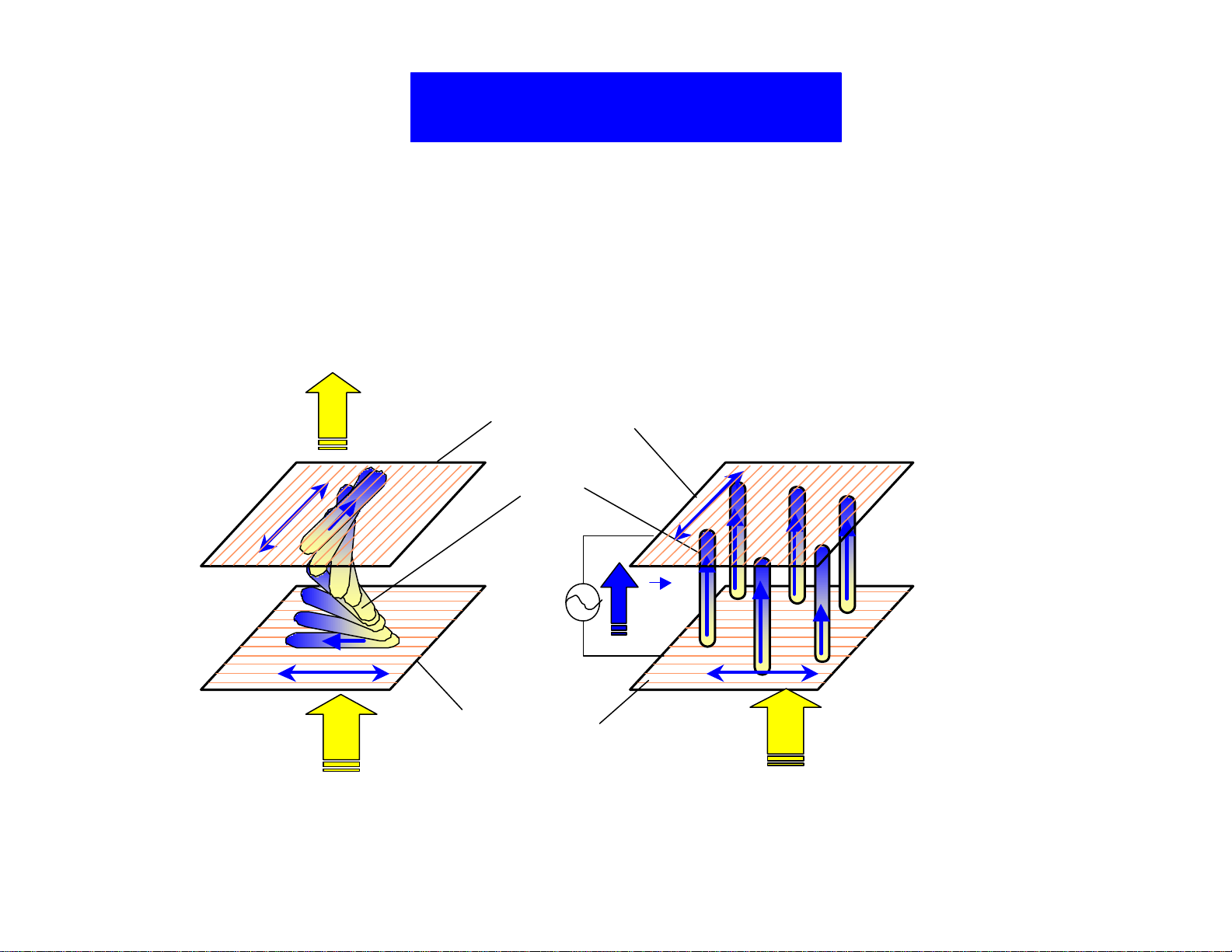
Active Addressing of (3x3) Matrix
t
Gate
Selection
t
-5V
20V
Gn-1
Gn
V1
+
V2
-
V3
Off Off Off
+
On On On
V1
V2
-
Off Off Off
+
Storage
Capacitor (Cs)
Pixel Electrode
(ITO)
+
V3
Line-by-Line
Addressing
-5V
Gn+1
Figure 29. An example of a (3x3) matrix pixel
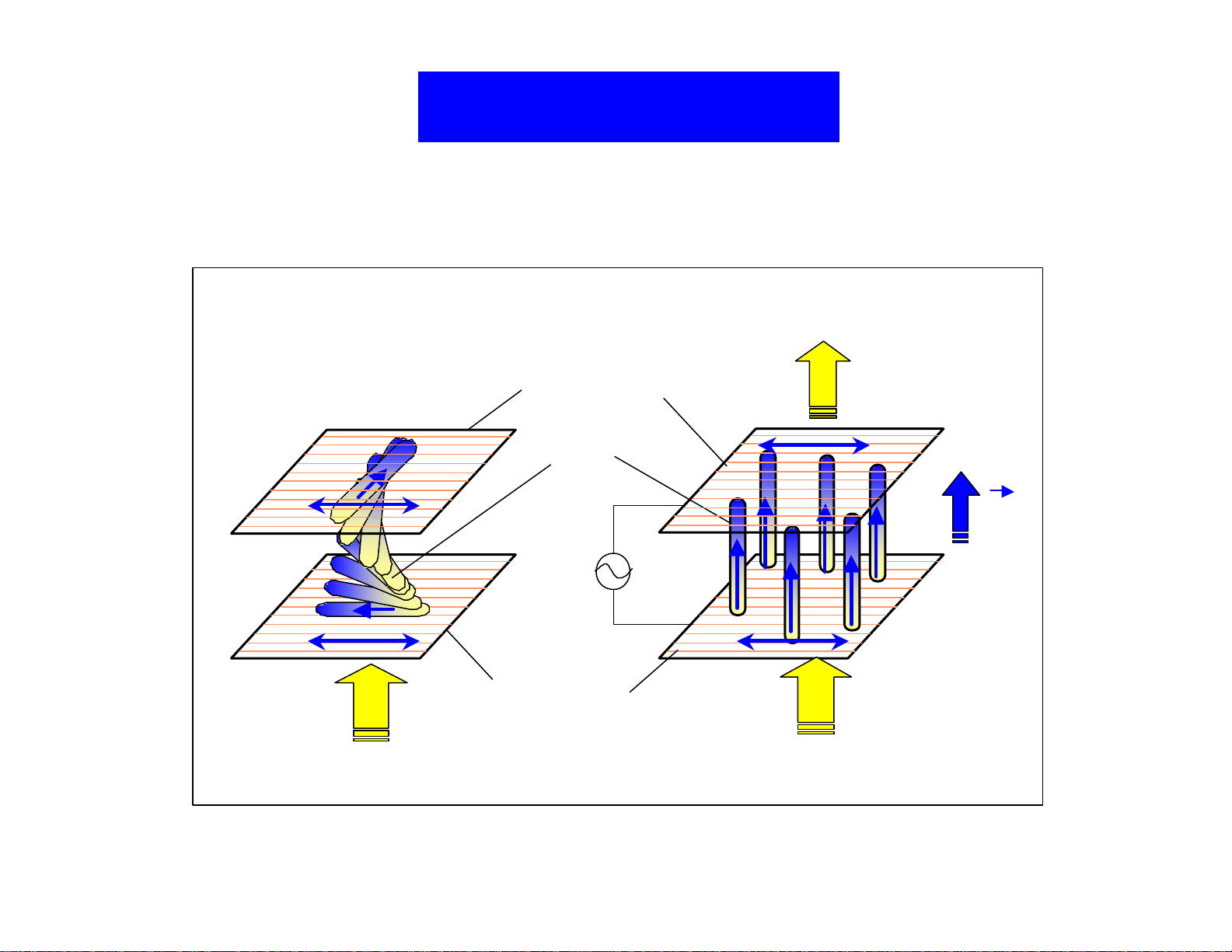
Page 39

G1
Animation of a (3x3) Matrix
V11 V12 V13
V21 V22 V23
V31 V32 V33
V11 V12 V13
V11 V12 V13
V11 V12 V13
Odd Frame
Odd Frame
Odd Frame
G3
V21 V22 V23
V21 V22 V23
V31 V32 V33
Page 40

Driving of LCD Panel
LCD Module
Data Signal
DC Power
DC/DC
Converter
Control
ASIC
LDI: LCD Driving IC
Source Driver IC’s
Gate Driver IC’s
Pixel
Electrode
TFT
LCD Panel
Inverter
Backlight Lamp
Figure 30. Driving of an LCD panel
Page 41

Representation of Image on LCD
multiplexing
0 0 0 0 0 0 0 0 0
0 0 0 0 0 0 0 0 0
0 0 0 1 1 1 1 1 0
0 0 1 0 0 0 1 1 0
0 1 0 0 0 1 0 1 0
1 1 1 1 1 0 0 1 0
1 0 0 0 1 0 1 0 0
1 0 0 0 1 1 0 0 0
1 1 1 1 1 0 0 0 0
Bit Image
in Memory
Figure 31. Representation of an image on an LCD
Pixels displayed
on Screen
Page 42

Parasitic Capacitance of TFT
• Staggered Structure
• Process Margin
W
L
Data Line
Gate Bus -Line
SourceDrain
Data Bus-Line
Pixel ITO
Common Electrode
Source
Cgs
(C/F Substrate)
Cds
Cs
Drain
Cgd
Gate Bus-Line
Clc
Gate
∆L
∆L Overlap (not avoidable)
Figure 32. Parasitic capacitors of a TFT
Page 43

Wave Forms of Pixel Driving Voltages
Cgd
Kickback Voltage
2Tf
1
<Vlc>eff = { Vp(t)-Vcom} dt
2 Tf
?
t=0
2
Tf = 1/60 sec
Odd Frame
Vg
On
∆ V
On Off
Vd
Vlc >Vcom
∆ V = x V
(Clc + Cs + Cgd)
+
-
Vd + Vd
Voffset = - Vcom
2
Tf = 1/60 sec
Even Frame
+
Vd + Vd
p -p
-
2
Vlc <Vcom
Vp(t)
Voffset
Vcom
∆ V
Figure 33. Driving a pixel and the effect of the parasitic capacitance
Page 44

Polarity Inversion Driving & Flickering
Driving Method
Frame
Inversion
H -Line
Inversion
2nd frame 3rd frame1st frame
Dot
Inversion
(Flicker free)
Figure 34. Polarity inversion driving methods
Page 45

Gray Scale Generation
D2
White
(101)(111) (000)
T
V1
T
1
V2
1 1 1 1 0 0 0 0
2
T3T
V3
4
V5
V4
T
5
(011)
T
6
V6
T7T
V7
V8
8 Gray-scale
8
Black
L/C Voltage
Transmittance
T1
T2
T7
T8
V1 V8V2 V7
...
D1
D0
1 1 0 0 1 1 0 0
1 0 1 0 1 0 1 0
Figure 35. A gray-scale example of the 3-bit LDI
L/C Voltage (V)
Digital Data
(3-bit)
23 = 8 gray scales
Page 46

Total # of Colors
n n n 3n
# of Color = 2 (R) x 2 (G) x 2 (B) = 2
n= # of data bits of LDI chip
3 bit = 8- gray/RGB = 512 colors
4 bit = 16- gray/RGB = 4,096 colors
ü6 bit = 64- gray/RGB = 262,144 colors
8 bit = 256- gray/RGB = 16,777,216 colors
Analog IC = Continuous gray-scale = full color
Figure 36. Total number of LCD colors
R
G
B
26=64
218=262,144
Page 47

Increasing Number of Gray Shades
Dithering
6 5
5 3/4 5 2/4 5 1/4
(2x2)
Unit Pixel
Reduced
Resolution
Frame Rate
Control
(FRC)
1st 2nd 3rd 4th frame
5
6
Figure 37. Dithering and frame rate control driving methods
+
+
+
+
+
+
+
+
+
+
+
+
+
+
+
=
=
=
=
=
Average
5
5 1/4
5 2/4
5 3/4
6
Page 48

Gray Scale with a Linear L/C Voltage
Trans. (%)
100
50
0
Trans. (%)
V8
V7
V6
V5
V4
V3
V2
V1
1.0 2.0 3.00
100
50
0
1
2 7
3 4 5 6 8
L/C Voltage (V)
Gray Scale
Figure 38. Gray-scale generation with a linear L/C voltage
Page 49

Optimization of Gray Scale Curve
Trans. (%)
V9
100
50
0
Trans. (%)
100
V8
V7
V6
V5
V4
V3
V2
V1
1.0 2.0 3.00
50
0
1
2 7
3 4 5 6 8
L/C Voltage (V)
Gray Scale
Figure 39. A gray-scale curve with an adjusted L/C voltage level
Page 50

γ −Correction of Gray Scale
Trans. (%)
100
50
γ
T = Tmax x ( gray # /Max. Gray)
γ = 1.0
• Light Sensitivity of Human Eye
0
γ = 2.2
γ = 3.0
16 32 48 64
Gray Scale
Figure 40. Gamma correction of the gray-scale curve
Page 51

Color Generation
Backlight
Spectra
400 500 600 700
TFT-Array
R G B
Color-Filter
Backlight
Color-Filter
Spectra
Transmitted
Lights
B
400 500 600 700
B
400 500 600 700
G
R
G
400 600 700
500 600 700
R
Figure 41. The color generation of the LCD
Page 52

Pixel Size and Resolving Power of Human Eye
• 10.4 inch VGA : 0.110mm x 0.330mm ( 77dpi )
• 12.1 inch SVGA : 0.1025mm x 0.3075mm ( 83dpi )
• 15.0 inch XGA : 0.099mm x 0.297mm (117dpi )
• 17.0 inch SXGA : 0.090mm x 0.270mm ( 94dpi )
• 21.3 inch UXGA : 0.090mm x 0.270mm ( 94dpi )
dpi : dot per inch
θ < 0.03° mixed color
Retina
~0.1mm
θ ~ 0.02°
~30cm
~0.1mm
Sub-Pixel
R G B
Figure 42. Color mix of RGB sub-pixel in the LCD panel
~0.3mm
Page 53

R G B
Arrangement of RGB
R G B
B R G
G B R
R G B
Array Design
C/F Fab.
R G B
R G B
R G B
Stripe Mosaic Delta
R G B
R G B
R G B
Simple
Simple
R
R
R
R G B
R G B
B
G B
R G B
Simple
Difficult
R G B
R G B
R G
R
R G B
B
R G B
R G B
R
R GB
Complex
Difficult
G
R
B
R
B
R
Driving CKT
Color Mix
Simple
Poor / w. low res.
Complex
Good
Figure 43. Arrangement of the RGB color-filter
Simple
Best
Page 54

Representation of Color
Primary Colors
Red (R)
Green(G)
Blue(B )
Color Coordinates
B
A color = rR + gG + bB
• r = R /(R + G + B )
• g = G /(R + G + B )
• b = B /(R + G + B )
with r + g + b = 1
Figure 44. The color coordinates
R
r
b
(r, g, b)
g
Y
(x, y)
G
X
Page 55

CIE Color Coordinates
• Color Balance
B
(0.21, 0.71)
G
W
(0.14, 0.08)
NTSC
(a)
(b)
(0.67, 0.33)
R
• Color Reproducibility
or Color Saturation
• Color Temperature
Color Reproducibility of
Display (a) =
Area of ∆ (a)
X 100%
Area of ∆ (NTSC)
Figure 45. The CIE color coordinates
 Loading...