

Samsung spl4225k service manual
PLASMA DISPLAY TV
Chassis : D53A
Model: SPL4225X/XAA
PLASMA DIAPLAY TV CONTENTS
Precautions
Reference Information
Specifications
Alignment and Adjustments
Circuit Operation Description
Troubleshooting
Exploded View and Parts List
Electric Parts List
Handling Description
Glossary
Wiring Diagram
Schematic Diagrams
1.
2.
3.
4.
5.
6.
7.
8.
9.
10.
11.
12.

ELECTRONICS
© Samsung Electronics Co., Ltd. FEB. 2002
Printed in Korea
AA82-
1. Precautions
1-1 Safety Precautions
1. Be sure that all of the built-in protective
devices are replaced. Restore any missing
protective shields.
2. When reinstalling the chassis and its
assemblies, be sure to restore all protective
devices, including: nonmetallic control knobs
and compartment covers.
3. Make sure that there are no cabinet openings
through which people—particularly
children—might insert fingers and contact
dangerous voltages. Such openings include
the spacing between fornt cabinet and back
cabinet, excessively wide cabinet
ventilation slots, and improperly fitted back
covers.
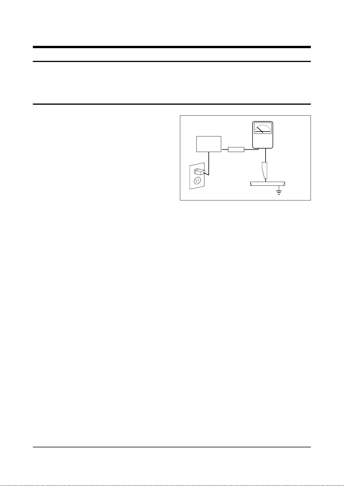
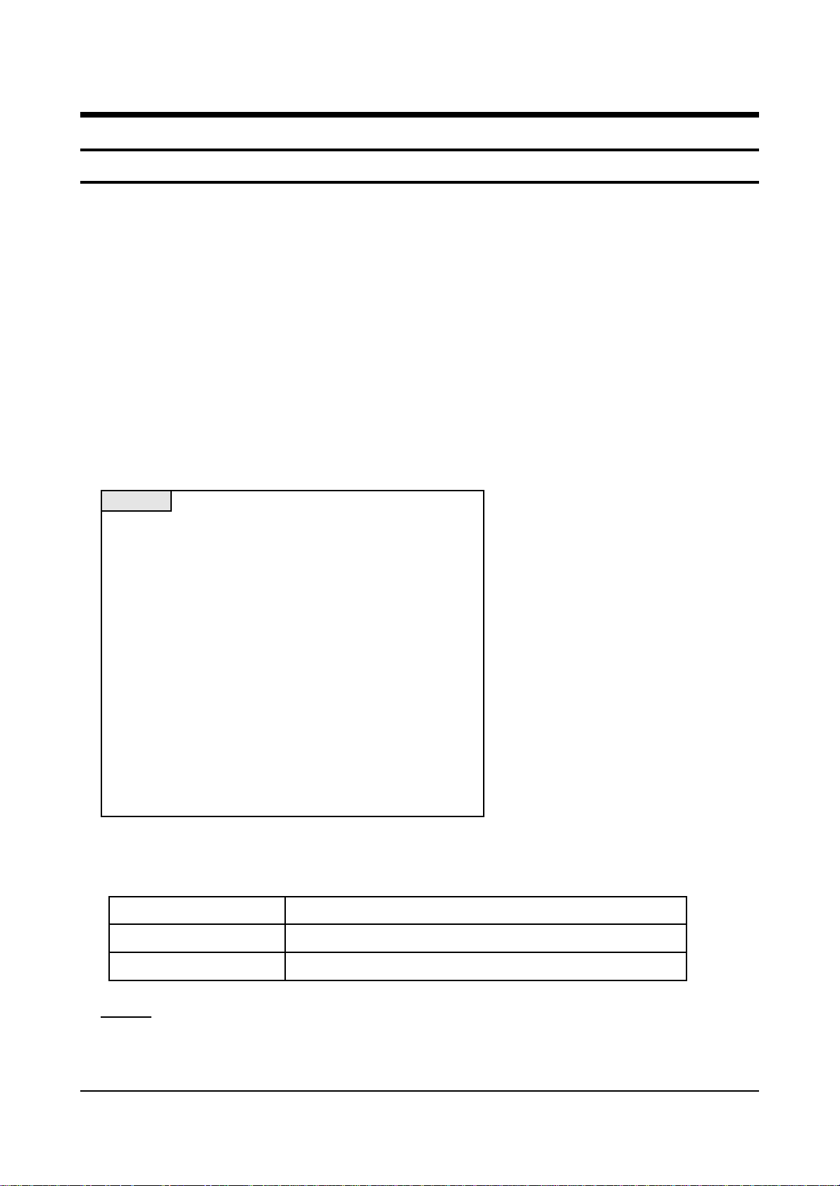
4. Leakage Current Hot Check (Figure 1-1):
Warning: Do not use an isolation
transformer during this test. Use a leakagecurrent tester or a metering system that
complies with American National Standards
Institute (ANSI C101.1, Leakage Current for
Appliances), and Underwriters Laboratories
(UL Publication UL1950.5.2).
5. With the unit completely reassembled, plug
the AC line cord directly into the power
outlet. With the unit’s AC switch first in the
ON position and then OFF, measure the
current between a known earth ground (metal
water pipe, conduit, etc.) and all exposed
metal parts, including: antennas, handle
brackets, metal cabinets, screwheads and
control shafts. The current measured should
not exceed 3.5 milliamp. Reverse the powerplug prongs in the AC outlet and repeat the
test.
Fig. 1-1 AC Leakage Test
6. Antenna Cold Check:
With the unit’s AC plug disconnected from the
AC source, connect an electrical jumper across
the two AC prongs. Connect one lead of the
ohmmeter to an AC prong. Connect the other
lead to the coaxial connector.
7. High Voltage Limits:
High voltage must be measured each time servicing is done on the B+, horizontal deflection
or high voltage circuits.
Precautions
Samsung Electronics 1-1
LEAKAGE
CURRENT
TESTER
DEVICE
UNDER
TEST
TEST ALL
EXPOSED METAL
SURFACES
2-WIRE CORD
ALSO TEST WITH
PLUG REVERSED
(USING AC ADAPTER
PLUG AS REQUIRED)
EARTH
GROUND
(READING SHOULD
NOT BE ABOVE
0.5mA)
Follow these safety, servicing and ESD precautions to prevent damage and protect against potential
hazards such as electrical shock and X-rays.

1-2 Safety Precautions (Continued)
8. High voltage is maintained within specified
limits by close-tolerance, safety-related
components and adjustments. If the high
voltage exceeds the specified limits, check
each of the special components.
9. Design Alteration Warning:
Never alter or add to the mechanical or
electrical design of this unit. Example: Do not
add auxiliary audio or video connectors. Such
alterations might create a safety hazard. Also,
any design changes or additions will void the
manufacturer’s warranty.
10. Hot Chassis Warning:
Some TV receiver chassis are electrically
connected directly to one conductor of the AC
power cord. If an isolation transformer is not
used, these units may be safely serviced only
if the AC power plug is inserted so that the
chassis is connected to the ground side of the
AC source.
To confirm that the AC power plug is inserted
correctly, do the following: Using an AC
voltmeter, measure the voltage between the
chassis and a known earth ground. If the
reading is greater than 1.0V, remove the AC
power plug, reverse its polarity and reinsert.
Re-measure the voltage between the chassis
and ground.
11. Some TV chassis are designed to operate with
85 volts AC between chassis and ground,
regardless of the AC plug polarity. These units
can be safely serviced only if an isolation
transformer inserted between the receiver and
the power source.
12. Some TV chassis have a secondary ground
system in addition to the main chassis ground.
This secondary ground system is not
isolated from the AC power line. The two
ground systems are electrically separated by
insulating material that must not be defeated
or altered.
13. Components, parts and wiring that appear to
have overheated or that are otherwise
damaged should be replaced with parts that
meet the original specifications. Always
determine the cause of damage or overheating, and correct any potential hazards.
14. Observe the original lead dress, especially
near the following areas: Antenna wiring,
sharp edges, and especially the AC and high
voltage power supplies. Always inspect for
pinched, out-of-place, or frayed wiring. Do
not change the spacing between components
and the printed circuit board. Check the AC
power cord for damage. Make sure that leads
and components do not touch thermally hot
parts.
15. Product Safety Notice:
Some electrical and mechanical parts have
special safety-related characteristics which
might not be obvious from visual inspection.
These safety features and the protection they
give might be lost if the replacement component differs from the original—even if the
replacement is rated for higher voltage,
wattage, etc.
Components that are critical for safety are
indicated in the circuit diagram by shading,
( ) or ( ).
Use replacement components that have the
same ratings, especially for flame resistance
and dielectric strength specifications.
A replacement part that does not have the
same safety characteristics as the original
might create shock, fire or other hazards.
Precautions
1-2 Samsung Electronics

1-3 Servicing Precautions
1. Servicing precautions are printed on the
cabinet. Follow them.
2. Always unplug the unit’s AC power cord from
the AC power source before attempting to: (a)
Remove or reinstall any component or
assembly, (b) Disconnect an electrical plug or
connector, (c) Connect a test component in
parallel with an electrolytic capacitor.
3. Some components are raised above the printed
circuit board for safety. An insulation tube or
tape is sometimes used. The internal wiring is
sometimes clamped to prevent contact with
thermally hot components. Reinstall all such
elements to their original position.
4. After servicing, always check that the screws,
components and wiring have been correctly
reinstalled. Make sure that the portion around
the serviced part has not been damaged.
5. Check the insulation between the blades of the
AC plug and accessible conductive parts
(examples: metal panels, input terminals and
earphone jacks).
6. Never defeat any of the B+ voltage interlocks.
Do not apply AC power to the unit (or any of
its assemblies) unless all solid-state heat sinks
are correctly installed.
7. Always connect a test instrument’s ground
lead to the instrument chassis ground before
connecting the positive lead; always remove
the instrument’s ground lead last.
8. Plasma display panels have partial afterimages when a same picture continues to be displayed for a certain time. This happens due to
the degradation of brightness caused by a
scale-down effect.
To prevent such afterimages when displaying
a same picture for a certain time, be sure to
reduce the level of brightness and contrast.
ex) Contrast : 50 or 75, Brightness : 25
9. Plasma display is an array of pixels(cells).
Therefore, if at least 99.9% pixels keep normal,
the appropriate panel is judged as ‘approved
product.’ Even though some of pixels keep
luminescent or always light off, do not worry
because the panel is approved.
Precautions
Samsung Electronics 1-3
Warning 1 : First read the “Safety Precautions” section of this manual. If some unforeseen circumstance creates a
conflict between the servicing and safety precautions, always follow the safety precautions.
Warning 2 : An electrolytic capacitor installed with the wrong polarity might explode.
1-4 Precautions for Electrostatically Sensitive Devices (ESDs)
1. Some semiconductor (“solid state”) devices
are easily damaged by static electricity. Such
components are called Electrostatically
Sensitive Devices (ESDs); examples include
integrated circuits and some field-effect
transistors. The following techniques will
reduce the occurrence of component damage
caused by static electricity.
2. Immediately before handling any semicon
ductor components or assemblies, drain the
electrostatic charge from your body by
touching a known earth ground. Alternatively,
wear a discharging wrist-strap device. (Be
sure to remove it prior to applying power—
this is an electric shock precaution.)
3. After removing an ESD-equipped assembly,
place it on a conductive surface such as
aluminum foil to prevent accumulation of
electrostatic charge.
4. Do not use freon-propelled chemicals. These
can generate electrical charges that damage
ESDs.
5. Use only a grounded-tip soldering iron when
soldering or unsoldering ESDs.
6. Use only an anti-static solder removal device.
Many solder removal devices are not rated as
“anti-static”; these can accumulate sufficient
electrical charge to damage ESDs.
7. Do not remove a replacement ESD from its
protective package until you are ready to
install it. Most replacement ESDs are
packaged with leads that are electrically
shorted together by conductive foam,
aluminum foil or other conductive materials.
8. Immediately before removing the protective
material from the leads of a replacement ESD,
touch the protective material to the chassis or
circuit assembly into which the device will be
installed.
9. Minimize body motions when handling
unpackaged replacement ESDs. Motions such
as brushing clothes together, or lifting a foot
from a carpeted floor can generate enough
static electricity to damage an ESD.
Precautions
1-4 Samsung Electronics
CAUTION
These servicing instructions are for use by
qualified service personnel only.
To reduce the risk of electric shock do not
perform any servicing other than that contained
in the operating instructions unless you are
qualified to do so.
Reference Information
Samsung Electronics 2-1
2. Reference Information
2-1 Tables of Abbreviations and Acronyms
A
Ah
Å
dB
dBm
°C
°F
°K
F
G
GHz
g
H
Hz
h
ips
kWh
kg
kHz
kΩ
km
km/h
kV
kVA
kW
I
MHz
Ampere
Ampere-hour
Angstrom
Decibel
Decibel Referenced to One
Milliwatt
Degree Celsius
Degree Fahrenheit
degree Kelvin
Farad
Gauss
Gigahertz
Gram
Henry
Hertz
Hour
Inches Per Second
Kilowatt-hour
Kilogram
Kilohertz
Kilohm
Kilometer
Kilometer Per Hour
Kilovolt
Kilovolt-ampere
Kilowatt
Liter
Megahertz
MV
MW
MΩ
m
µA
µF
µH
µm
µs
µW
mA
mg
mH
mI
mm
ms
mV
nF
Ω
pF
Ib
rpm
rps
s
V
VA
W
Wh
Megavolt
Megawatt
Megohm
Meter
Microampere
Microfarad
Microhenry
Micrometer
Microsecond
Microwatt
Milliampere
Milligram
Millihenry
Milliliter
Millimeter
Millisecond
Millivolt
Nanofarad
Ohm
Picofarad
Pound
Revolutions Per Minute
Revolutions Per Second
Second (Time)
Volt
Volt-ampere
Watt
Watt-hour
Table 2-1 Abbreviations
Reference Information
2-2 Samsung Electronics
Table 2-2 Table of Acronyms
ABL
AC
ACC
AF
AFC
AFT
AGC
AM
ANSI
APC
APC
A/V
AVC
BAL
BPF
B-Y
CATV
CB
CCD
CCTV
Ch
CRT
CW
DC
DVM
EIA
ESD
ESD
FBP
FBT
FF
FM
FS
GND
G-Y
H
HF
HI-FI
IC
IC
IF
Automatic Brightness Limiter
Alternating Current
Automatic Chroma Control
Audio Frequency
Automatic Frequency Control
Automatic Fine Tuning
Automatic Gain Control
Amplitude Modulation
American National Standards Institute
Automatic Phase Control
Automatic Picture Control
Audio-Video
Automatic Volume Control
Balance
Bandpass Filter
Blue-Y
Community Antenna Television (Cable TV)
Citizens Band
Charge Coupled Device
Closed Circuit Television
Channel
Cathode Ray Tube
Continuous Wave
Direct Current
Digital Volt Meter
Electronics Industries Association
Electrostatic Discharge
Electrostatically Sensitive Device
Feedback Pulse
Flyback Transformer
Flip-Flop
Frequency Modulation
Fail Safe
Ground
Green-Y
High
High-Frequency
High Fidelity
Inductance-Capacitance
Integrated Circuit
Intermediate Frequency
I/O
L
L
LED
LF
MOSFET
MTS
NAB
NEC
NTSC
OSD
PCB
PLL
PWM
QIF
R
RC
RF
R-Y
SAP
SAW
SIF
SMPS
S/N
SW
TP
TTL
TV
UHF
UL
UV
VCD
VCO
VCXO
VHF
VIF
VR
VTR
VTVM
TR
Input/output
Left
Low
Light Emitting Diode
Low Frequency
Metal-Oxide-Semiconductor-Field-Effect-Tr
Multi-channel Television Sound
National Association of Broadcasters
National Electric Code
National Television Systems Committee
On Screen Display
Printed Circuit Board
Phase-Locked Loop
Pulse Width Modulation
Quadrature Intermediate Frequency
Right
Resistor & Capacitor
Radio Frequency
Red-Y
Second Audio Program
Surface Acoustic Wave(Filter)
Sound Intermediate Frequency
Switching Mode Power Supply
Signal/Noise
Switch
Test Point
Transistor Transistor Logic
Television
Ultra High Frequency
Underwriters Laboratories
Ultraviolet
Variable-Capacitance Diode
Voltage Controlled Oscillator
Voltage Controlled Crystal Oscillator
Very High Frequency
Video Intermediate Frequency
Variable Resistor
Video Tape Recorder
Vacuum Tube Voltmeter
Transistor
Specifications
Samsung Electronics 3-1
3. Specifications
MODEL
3-1 Display(PDP Monitor)
Display
Remote Control
Display
Remote Control
Voltage
Power Consumption
Number of Pixels
Screen Size
AUDIO Input
AUDIO Output
VIDEO Input
Dimensions
(mm/inch)
Weight
SPL4225
1038.8(W) x 89(D) x 635(H)mm / 40.9(W) x 3.5(D) x 25(H) Inches
54(W) x 31.5(D) x 220(H)mm / 2.13(W) x 1.24(D) x 8.66(H) Inches
32Kg / 70.55\bs
150g (Including batteries) / 0.33\bs
AC 100-240V, 50/60Hz
310 Watts
852(H) X 480(V)
106Cm / 42 Inches
VIDEO / S-VIDEO
COMPONENT 1
COMPONENT 2
PC (RGB)
7W + 7W (8Ω)
VIDEO
S-VIDEO
COMPONETN 1 -480i / 480p
COMPONETN 2 -480p~1080i
PC (RGB)

3-2 Samsung Electronics
MENO
Alignment and Adjustments
Samsung Electronics 4-1
4. Alignment and Adjustments
4-1 Service Mode
4-1-1 SERVICE MODE ENTRY METHOD (General Transmitter)
1. Turn off the power to make the SET STAND-BY mode.
2. In order to enter the Service Mode, select MUTE-1-8-2-POWER.
S In case entry into SERVICE MODE is unsuccessful, repeat the procedures above.
4-1-2 Initial DISPLAY State in times of SERVICE MODE Switch overs
4-1-2(A) OSD DISPLAY
4-1-2(B) BUTTONS OPERATIONS WITHIN SERVICE MODE
#Notice
1. In case of no signal in ALL MODE. entry into the FACTORY MODE cannot be made.
1. PWS364 - Video
2. SDA9280 - Video
3. VPC3230 - Video
4. SDA9400 - Video
5. CXA2101 - Video /HSComponent
6. AD9884
7. OSD Position
8. Option
9. Reset
10. Aging
Release Time :
Menu
Joystick UP/DOWN
Joystick (LEFT/RIGHT)
Entire menu display
Cursor move to select items
Enable to increase and decrease the data of the selected items
MENU
Alignment and Adjustments
4-2 Samsung Electronics
4-1-3 Details of Control
4-1-3(A) PW364
No OSD Range
1
2
3
4
Horizontal Size
Vertical Size
Horizontal Pos
Vertical Pos
0 ~ 255
0 ~ 255
0 ~ 255
0 ~ 255
DO NOT ENTER
DO NOT ENTER
DO NOT ENTER
DO NOT ENTER
4-1-3(B) SDA9280
Default of MODE
VIDEO / S-VHS /DVD 1080i 720p 480p PC
2
51
185
24
148 (Fix)
45
148 (Fix)
11
69
46
188
13
80
42
121
29
No OSD Range
1
2
3
4
5
6
7
8
CTI THRESH
CTI TRAWID
Y-DELAY
LPF GAIN
BPF GAIN
HPF GAIN
PHACOM
COR
0 ~ 15
0 ~ 12
0 ~ 15
0 ~ 7
0 ~ 15
0 ~ 15
0 ~ 2
0 , 1
Default of MODE
VIDEO / S-VHS /DVD DTV PC
DO NOT ENTER
DO NOT ENTER
DO NOT ENTER
DO NOT ENTER
DO NOT ENTER
DO NOT ENTER
DO NOT ENTER
DO NOT ENTER
8
1
8
7
10
8
2
1
-
-
-
-
-
-
-
-

Alignment and Adjustments
Samsung Electronics 4-3
4-1-3(C) VPC3230
4-1-3(D) SDP9400
No OSD Range
1
2
3
4
5
6
7
8
9
10
11
12
13
14
Bright YUV
Cont YUV
IF Comp
Chroma band
Luma LPF
HPLL Speed
Luma Delay
3230 Bright
3230 Contrast
H LPF Y/C
H LPF Chroma
H Peak Filter
Peaking Gain
Coaring Off/On
0 ~ 255
0 ~ 63
0 ~ 3
0 ~ 3
0 , 1
0 ~ 3
0 ~ 8
0 ~ 255
0 ~ 63
0 ~ 3
0 , 1
0 ~ 2
0 ~ 7
0 , 1
Default of MODE
VIDEO / S-VHS /DVD DTV PC
DO NOT ENTER
DO NOT ENTER
DO NOT ENTER
DO NOT ENTER
DO NOT ENTER
DO NOT ENTER
DO NOT ENTER
DO NOT ENTER
DO NOT ENTER
DO NOT ENTER
DO NOT ENTER
DO NOT ENTER
DO NOT ENTER
DO NOT ENTER
195
29
0
3
1
1
8
146
42
0
0
2
4
1
-
-
-
-
-
-
-
-
-
-
-
-
-
-
No OSD Range
1
2
3
4
OUT DELAY
TNRCLY
TNRCNC
STOP MODE
0 ~ 255
0 ~ 15
0 ~ 15
0 ~ 7
Default of MODE
VIDEO / S-VHS /DVD DTV PC
DO NOT ENTER
DO NOT ENTER
DO NOT ENTER
DO NOT ENTER
10
0
10
3
-
-
-
-
Alignment and Adjustments
4-4 Samsung Electronics
1
2
3
4
5
6
7
8
9
10
11
12
13
14
15
16
17
Limit Level
System
D-Color
R Drive
G Drive
B Drive
R CutOff
G CutOff
B CutOff
ABL Mode
ABL TH
H Sep Sel.
Contrast
Bright
Cr Offset1
CB Offset1
Drive
4-1-3(E) CXA2101
No OSD Range Remarks
Default of MODE
VIDEO DTV
0 ~ 3
0 ~ 3
0 ~ 63
0 ~ 63
0 ~ 63
0 ~ 63
0 ~ 63
0 ~ 63
0 ~ 63
0 ~ 3
0 ~ 3
0 , 1
0 ~ 63
0 ~ 3
0 ~ 15
0 ~ 15
-
0
2
31
31
31
31
31
31
31
0
0
0
9
52
7
7
-
0
3
31
31
31
31
31
31
31
0
0
0
9
52
7
7
-
DO NOT
ENTER
18
19
20
21
22
23
24
25
26
27
28
29
30
31
32
33
Sub Bright
Sub Cont
Sub Color
Sub Hue
Sub SHP
R-Y/R
R-Y/B
G-Y/R
G-Y/B
PABL Level
SHP F0
Pre/over
CTI Level
LTI Level
DC-Tran
D-Pic
No OSD Range Remarks
Default of MODE
VIDEO DTV
-
0 ~ 15
0 ~ 15
0 ~ 15
0 ~ 3
0 ~ 15
0 ~ 15
0 ~ 15
0 ~ 15
0 ~ 15
0 ~ 3
0 ~ 3
0 ~ 3
0 ~ 3
0 ~ 3
0 ~ 3
38
9
9
5
2
8
12
7
4
6
3
0
1
0
1
2
40
8
10
5
3
4
9
5
7
6
3
2
1
0
1
1
DO NOT
ENTER
Alignment and Adjustments
Samsung Electronics 4-5
4-1-3(F) AD9884
No OSD Range
1
2
3
4
5
6
7
8
9
10
11
12
Red Gain
Green Gain
Blue Gain
Red Offset
Green Offset
Blue Offset
Gain Drive
Offset Drive
V Contrast
V Bright
Phase
Charge Pump
0 ~ 255
0 ~ 255
0 ~ 255
0 ~ 255
0 ~ 255
0 ~ 255
0 ~ 255
0 ~ 255
0 ~ 63
0 ~ 63
0 ~ 31
0 ~ 7
135
130 (Fix)
150
124
128 (Fix)
132
50
150
DO NOT ENTER
DO NOT ENTER
0 (Fix)
0 (Fix)
Default of MODE
VIDEO / S-VHS /DVD 1080i 720p 480p PC
134
130 (Fix)
141
125
128 (Fix)
113
DO NOT ENTER
DO NOT ENTER
30
42
15
0
3
142
130 (Fix)
136
125
128 (Fix)
119
36
38
15
4-1-3(G) OSD POSITION
No OSD Item Range Default Description
12Horiz
Vert
Horiz (Left,Right)
Vert (Up,Down)
-128 ~ +128
-24 ~ +24
40
16
Move 8 by 8 (Total: 33 Step), Fixed
Move 8 by 8 (Total: 7 Step), Fixed
134
130 (Fix)
141
125
128 (Fix)
113
2
DO NOT ENTER
DO NOT ENTER
30
42
15
0
Alignment and Adjustments
4-6 Samsung Electronics
4-1-3(H) OPTION
1
2
3
4
5
6
7
8
Back Ground Color
Shift Pixel
Pixel Shift Min
Pixel Shift SEC
Fan Protect
Temp Protect
Sharpness
Base Language
No OSD Range
Default of MODE
VIDEO / S-VHS /DVD PC
BLUE1 ↔ GREEN
0 ~ 8
0 Min ~ 59 Min
0 Sec ~ 59 Sec
Off ↔ On
Off ↔ On
0 ~ 15
English → Espania →
France → Korea → English
BLUE1
4
4 Min
0 Sec
Off
On
5
English
-
-
-
-
-
-
5
English
-
-
-
-
-
-
7
English
-
-
-
-
-
-
8
English
DTV
720p 1080i
Samsung Electronics 4-7
Alignment and Adjustments
4-1-4 White Balance Adjust Method
1. Press MUTE-1-8-2-POWER to enter the factory mode.
2. Enter "6. AD9884"
3. Adjust LOW coordinates as R,B OFFSET and HIGH coordinates as R,B GAIN. (GREEN is fixed)
4. In VIDEO,DTV mode, Adjust LOW light as "V BRIGHT".
5. In PC mode, Adjust LOW light as "OFFSET DRIVE".
6. In VIDEO,DTV mode, Adjust HIGH light as "V CONTRAST".
7. In PC mode, Adjust HIGH light as "GAIN DRIVE".
- W/B Adjustment SPEC(Suwon Factory Toshiba PATTERN)
√ VIDEO MODE
√ DTV MODE
Adjustment
Coordinates
H-LIGHT
L-LIGHT
Coordinates
Value
x : 279
y : 283
Y : 28.4[f\]
x : 297
y : 252
Y : 0.53[f\]
Adjustment
Deviation
±: 3
±: 3
±: 3
±: 5
±: 5
± : 0.1
Adjustment
Coordinates
H-LIGHT
L-LIGHT
Coordinates
Value
x : 274
y : 275
Y : 30.8[f\]
x : 313
y : 275
Y : 0.59[f\]
Adjustment
Deviation
±: 3
±: 3
±: 3
±: 5
±: 5
± : 0.1
Alignment and Adjustments
4-8 Samsung Electronics
√ PC MODE
Adjustment
Coordinates
H-LIGHT
L-LIGHT
Coordinates
Value
x : 280
y : 278
Y : 16.4[f\]
x : 298
y : 244
Y : 1.19[f\]
Adjustment
Deviation
±: 3
±: 3
±: 2
±: 5
±: 5
± : 0.1

Alignment and Adjustments
Samsung Electronics 4-9
Alignment and Adjustments
4-2 SPL4225 PC Input Mode
USER
V-Position
Factory
HP/VP/P
PHASE
CLOCK/
fO(Hz)
125/22/0/0
125/22/0/0
70.1
125/8/0/1
125/16/0/0
125/8/0/1
125/16/0/0
85
70.0
124/31/0/0
125/31/0/0
124/31/0/0
125/31/0/0
75
72.8
125/2/0/0
125/9/1/2
125/2/0/0
125/9/1/2
59.9
85.1
125/0/0/1
125/31/0/2
125/0/0/1
125/31/0/2
75
72.2
126/1/0/1
125/15/0/1
126/1/0/1
125/15/0/1
60.3
56.3
126/14/2/3
125/20/1/3
125/21/1/3
125/16/1/2
126/14/2/3
125/20/1/3
125/21/1/3
85
75
70.1
125/16/1/2
60
HFreqSec
/99=31.777
/99=31.777
HS1Period
31.777u/10.1n=3146.2
31.777u/10.1n=3146.2
Dot_c
V_P
H_P
VTotal
28.232
1
0
449
31.777
25.175
0
1
449
31.777
HFreqSes
=23.111
=26.666
=2288.21
=2640.29
36.0
31.5
0
0
0
0
509
500
23.111
26.667
=26.414
=31.777
=2615.14
=3146.23
31.5
25.175
0
0
0
0
520
525
26.413
31.777
=18.626
=21.333
=1844.65
=2112.17
49.5
56.25
1
1
1
1
631
625
18.631
21.333
=20.797
=26.393
=2059.4
=2613.86
50.0
40.0
1
1
1
1
666
628
20.800
26.400
=28.444
=14.555
=2816.23
=1441.68
36.0
94.5
1
1
625
808
28.444
14.561
=16.656
=17.707
=1649.50
=1753.16
78.75
75.000
1
0
1
0
800
806
16.660
17.707
=20.676
=2047.22
65.000
0
0
806
20.677
400
350
480
480
480
480
600
600
600
600
600
768
768
768
1024
14
768
1024
15
VRes
720
640
640
640
640
640
800
800
800
800
800
1024
12
1024
13
HRes
1
2
3
4
5
6
7
8
9
10
NO
11
Alignment and Adjustments
4-10 Samsung Electronics
Alignment and Adjustments
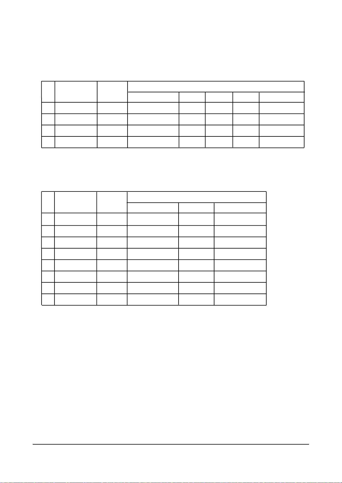
4-3 Discharge Voltage Adjustment Method (Monitor) in Times of ASS’Y Repair
and Replacement
-All VR (Variable Resistor), except for VR for Vs, voltage goes down when turned counterclockwise.
l Vsc and Vy Adjustment Method
l Vs and Va Adjustment Method
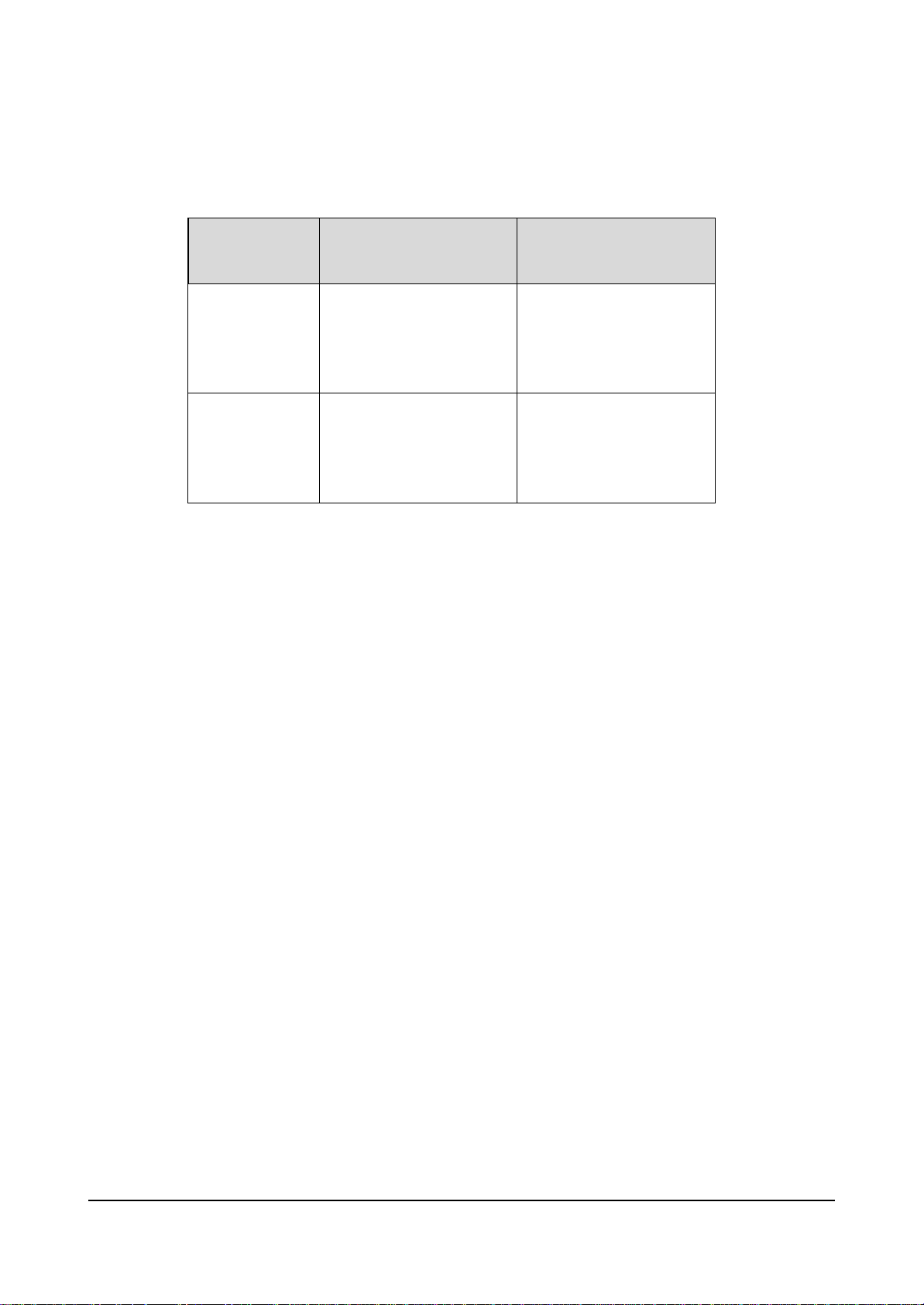
n Vsc is the voltage of the left terminal
for D5207
n Voltage adjustment is made for Vsc by
using VR5201
n Standard voltage for Vsc is –55V±10V
n Vy is the voltage of the right terminal
for D5207
n Voltage adjustment is made for Vy by
using VR5200
n Standard voltage for Vy is 132V±10V
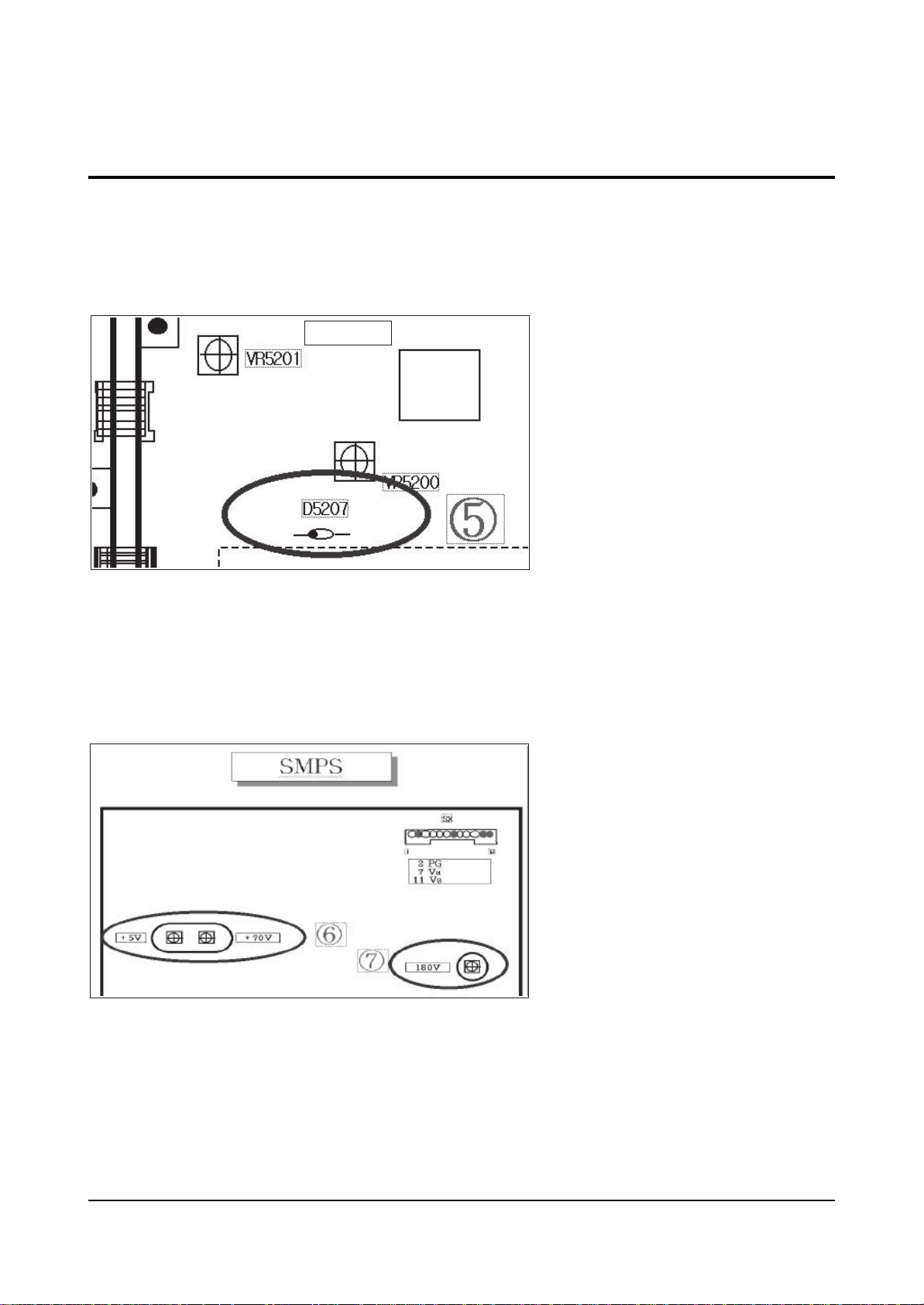
n Vs is the voltage of the no.11 PIN of SX
Connector.
n Voltage adjustment is made for Vs by
using VR in 7
n Vs is 175±5V
n Va is the voltage of the no.7 PIN of SX
Connector.
n Voltage adjustment is made for Va by
using right VR in 6
n Va is 75±5V
Y-Main
Alignment and Adjustments
Samsung Electronics 4-11
Alignment and Adjustments
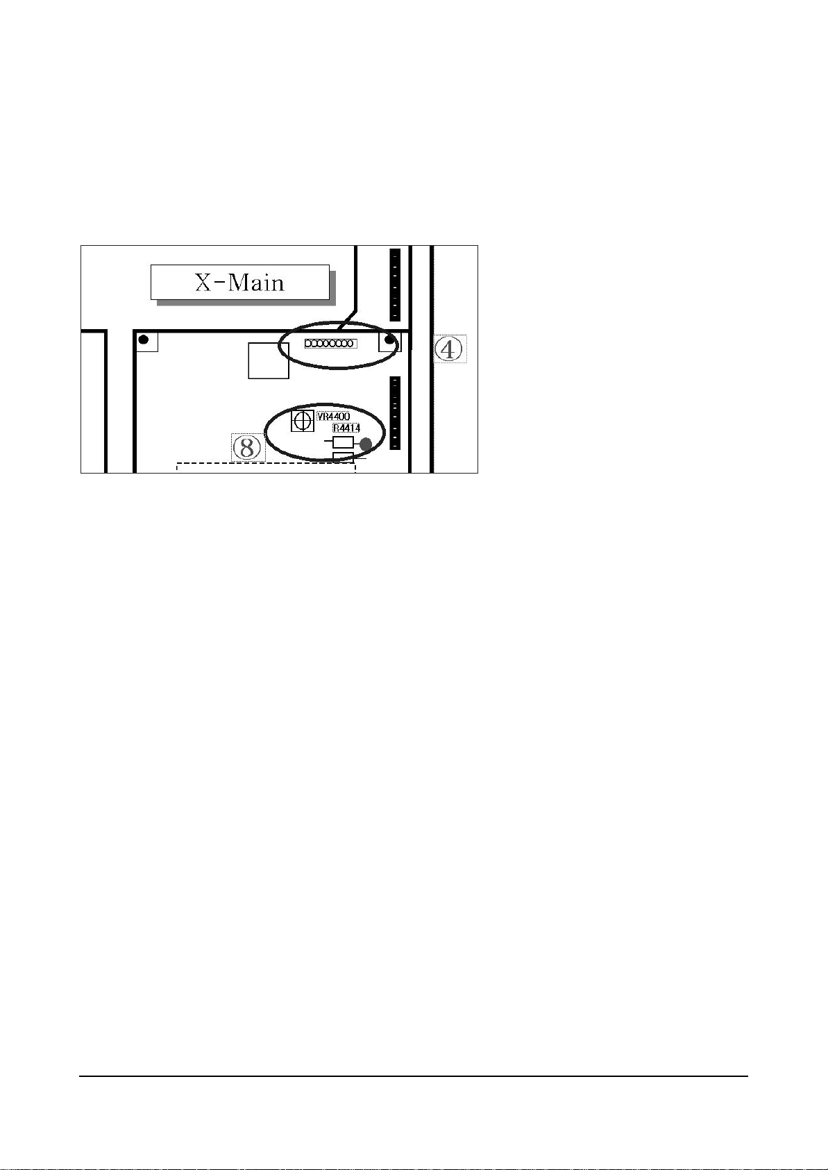
l Vw Adjustment Method
n Vw is the voltage of the right terminal
for R4414
n Voltage adjustment is made for Vw by
using VR4400
n Standard voltage for Vw is 175V±5V

Alignment and Adjustments
4-12 Samsung Electronics
Alignment and Adjustments
4-4 Fault Finding Using MULTI METER
Parts defects can be found for DIODE TRANSISTOR IC, using MULTI TEST including
Forward/Reverse direction Multi Test. Of course, in case resistance of several ohms and COIL are connected in parallel circuit, the lock out circuit parallel connected to part must be severed.
1.DIODE
2. TRANSISTOR
l For NPN(KSC815-Y, 2SC2068, 2SC2331-Y)
l For PNP(KSA539-Y)
Forward Direction
Hundreds of ohms
Reverse Direction
Infinity
Between Anode and Cathode
C (COLLECTOR)
E
B(BASE)
BC
C (COLLECTOR)
E
B(BASE)
BC
E (EMITTER)
E (EMITTER)
Forward Direction
Hundreds of ohms
Hundreds of ohms
Infinity
Reverse Direction
Infinity
Infinity
Infinity
Between B and E
Between B and C
Between E and C
Forward Direction
Hundreds of ohms
Hundreds of ohms
Infinity
Reverse Direction
Infinity
Infinity
Infinity
Between B and E
Between B and C
Between E and C
+- +-

Alignment and Adjustments
Samsung Electronics 4-13
Alignment and Adjustments
3. IC (INTEGRATED CIRCUIT)
IC has built in DIODE against overvoltage in PIN. Generally, except for internal circuit defects, IC defects
can be found, by measuring the DIODE.
› Defects have SHORT(0 ohm) for both forward and reverse direction.
Hundreds of ohms
Forward Direction
Reverse Direction
Varying depending on IC but generally normal
Infinity in DIODE TEST MODE

4-14 Samsung Electronics
MEMO

Troubleshooting
Samsung Electronics 6-1
6. Troubleshooting
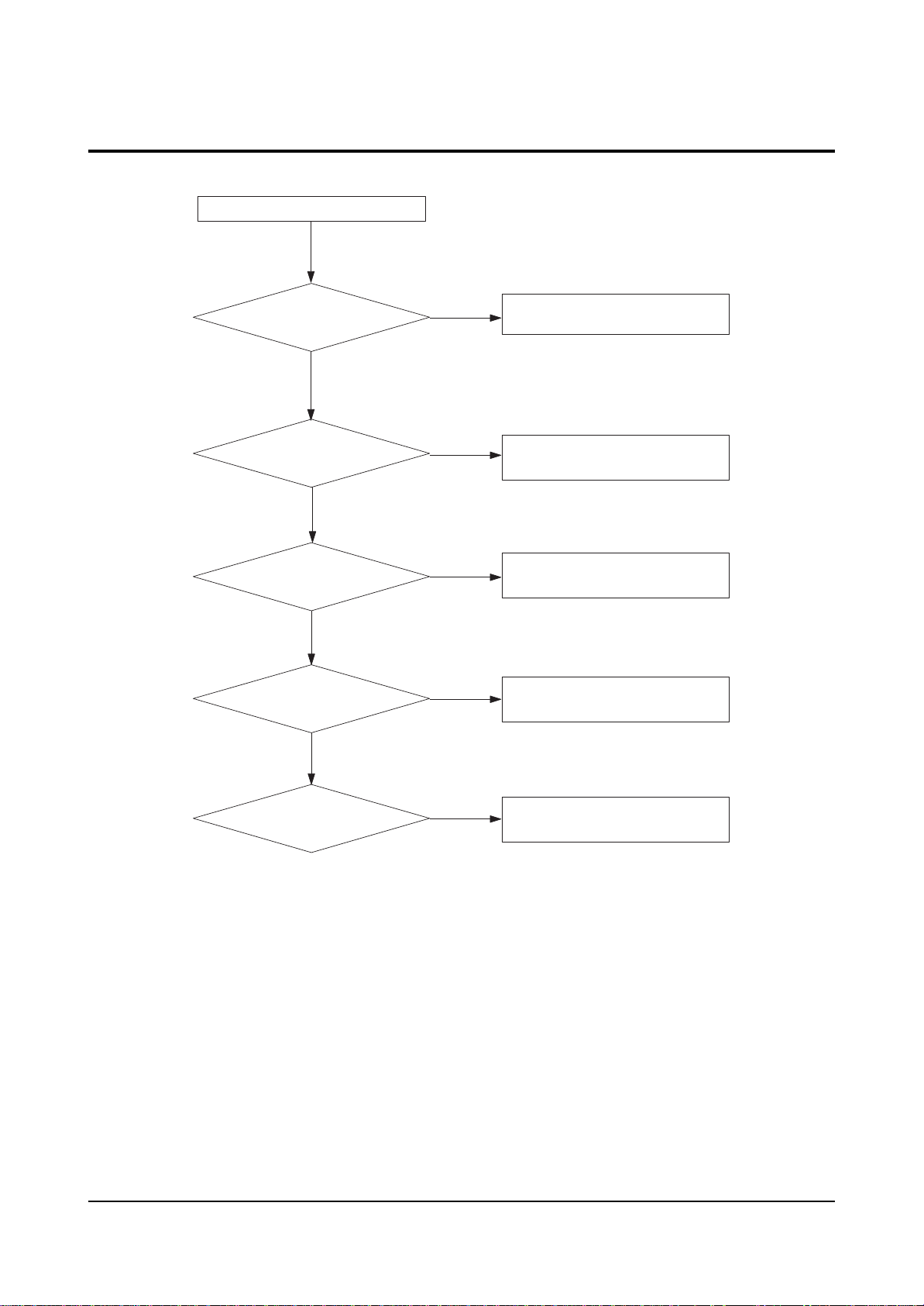
6-1 Entirely no screen
Remove SMPS output connector
(connect Video B d only)
Normal
Power on
Normal
SMPS Output
Voltage
Normal
Logic Connect Power
LED Light-on
(Power, Sink)
Normal
X-B d Connect Power
Abnormal
Abnormal
Abnormal
5V Output
Abnormal
AC Input
Normal
Replace SMPS
Replace Logic B d
Normal
Normal
Replace Video B d
Change Fuse
X-B d Output
Normal
Y-B d Connect Power
Y-B d Output
Normal
Replace Panel
Abnormal
Replace X-B d
Abnormal
Replace Y-B d
6-2 Samsung Electronics
Alignment and Adjustments
6-2 Partly no screen
Power on
Upper part no screen
No
Lower part no scree
No
1//14 Screen part
Abnormal
No
1/28 no screen
Yes
Yes
Yes
Yes
Replace Upper Scan Buffer B d
Replace Lower Scan Buffer B d
Replace Corresponding
Address Buffer B d
Replace Panel
No
1/7 no screen
Yes
Replace Panel
Troubleshooting
Samsung Electronics 6-3
6-3 Checking the Board (Unit)
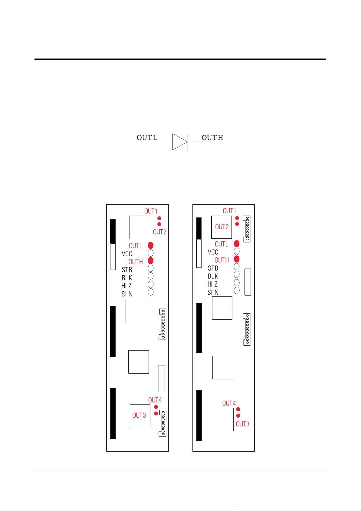
6-3-1 Y buffer
- To check the main board, you have to check the Y buffer first.
- After separating Y Main and Y buffer board,
- Check the Diode between OUTL and OUTH, and make sure that the forward voltage drop is between
0.4 and 0.5V.
- Check that the resistance between the two terminals is more than several kW.
Troubleshooting
6-4 Samsung Electronics
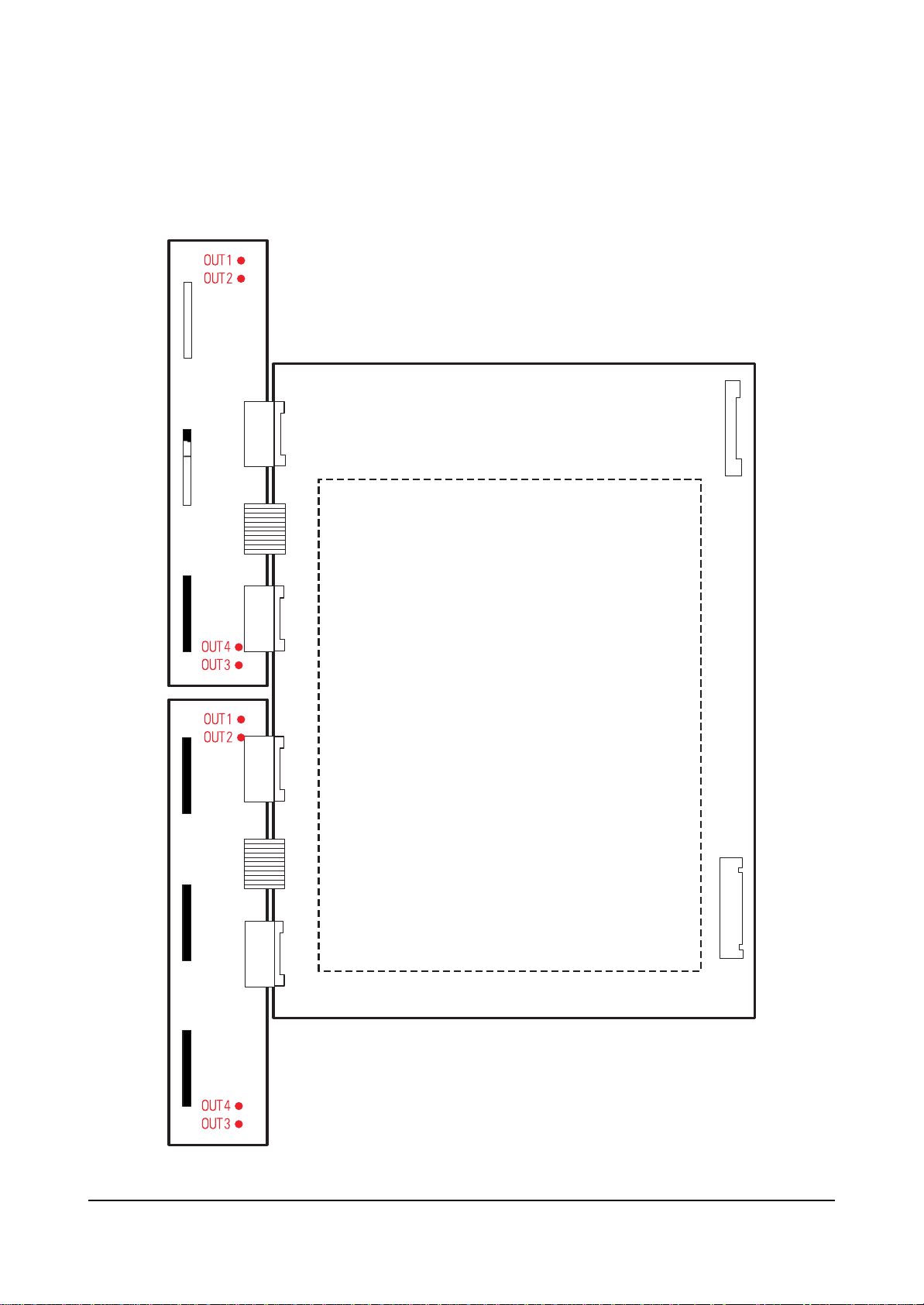
6-3-2 Y Main
- After connecting Y main and Y buffer board, check that one of the output waveforms from OUT 1, 2, 3
or 4 is the same as that of the appendix 1 when power is supplied.

Troubleshooting
Samsung Electronics 6-5
6-3-3 X Board
- Check that one of the output waveforms from X-OUT 1 or 2 is the same as that of the appendix 2
when power is supplied.
X- OUT1
X- OUT1
Troubleshooting
6-6 Samsung Electronics
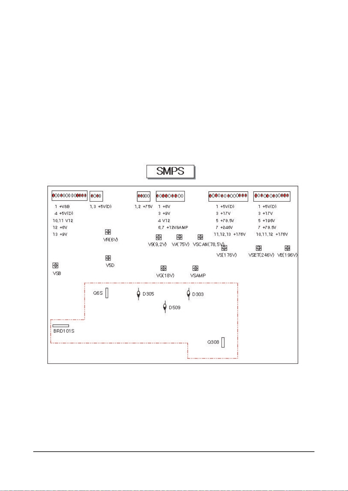
6-3-4 SMPS
- Check output voltage.
- If output voltage is not detected, check the following lists:
(1) Check fuse
(2) In case of +5V(D), check that D305 is short
(3) In case of VSAMP, check that D506 is short
(4) In case of VA, check that D303 is short
(5) In case of VS, check that pin 2 and 3 of Q303 are short
(6) In case of Q6S, check that pin 2 and 3 are short
(7) Check that BRD101S is short
 Loading...