

Page 1

2
CONTENTS
ⅠⅠ.. SSPPEECCIIFFIICCAATTIIOONN
1. CAMERA SPECIFICATION …………………………………………………………………………………………4
2. SYSTEM REQUIREMENTS ………………………………………………………………………………………5
3. TFT LCD PANEL MARK …………………………………………………………………………………………6
4. CONNECTION DIAGRAM …………………………………………………………………………………………8
5. IDENTIFICATION OF FEATURES …………………………………………………………………………………9
ⅡⅡ.. IINNSSTTAALLLLAATTIIOONN
………………………………………………………………………………………………11
ⅢⅢ.. EEXXPPLLOODDEEDD VVIIEEWW AANNDD PPAARRTTSS LLIISSTT
1. FORNT COVER ASSEMBLY ……………………………………………………………………………………18
2. MAIN ASSEMBLY…………………………………………………………………………………………………20
3. MIDDLE COVER ASSEMBLY ……………………………………………………………………………………22
4. BACK ASSEMBLY ………………………………………………………………………………………………24
5. PACKING ITEM……………………………………………………………………………………………………26
ⅣⅣ.. AADDJJUUSSTTMMEENNTT
1. Digital Camera Service ………………………………………………………………………………………29
2. How to check the FIRMWARE VERSION………………………………………………………………………35
3. How to check the FIRMWARE UPGRADE ……………………………………………………………………36
4. ADJUSTMENT ……………………………………………………………………………………………………38
ⅤⅤ.. PPAATTTTEERRNN DDIIAAGGRRAAMM
1. PARTS ARRANGEMENT FOR EACH PCB ASS’Y
1) MAIN_TOP ……………………………………………………………………………………………………47
2) MAIN_BOTTOM ………………………………………………………………………………………………48
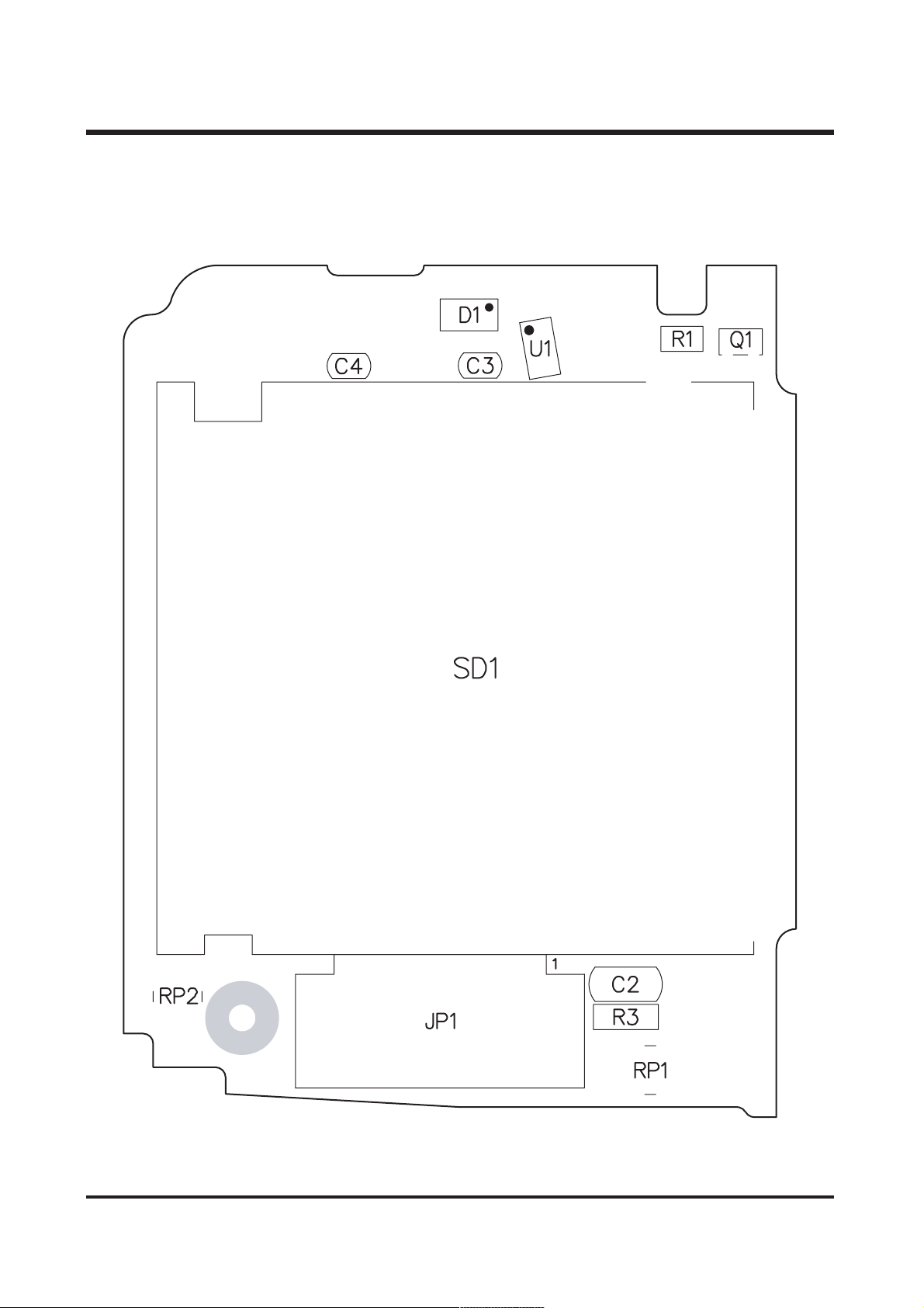
3) KEY_TOP ……………………………………………………………………………………………………49
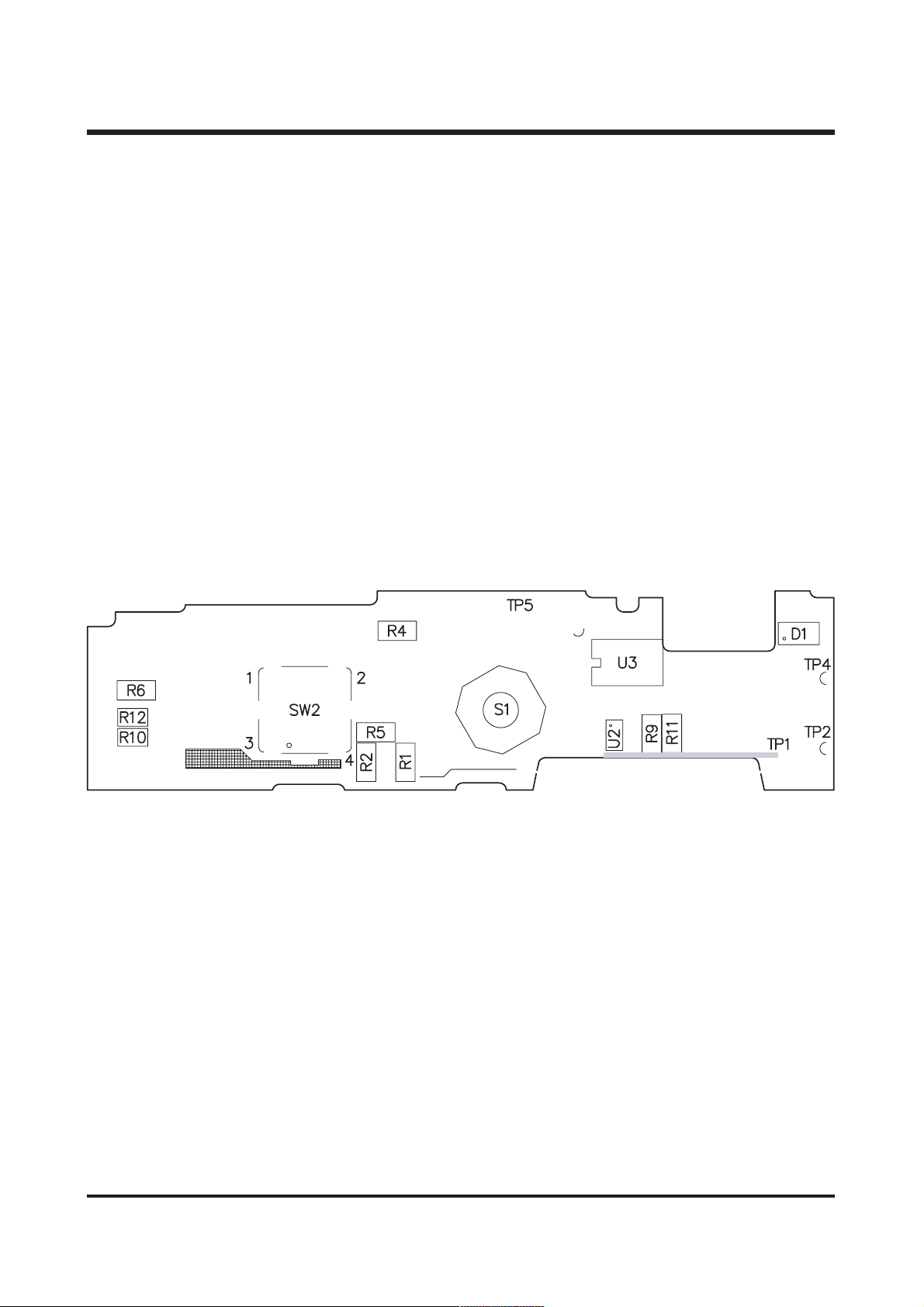
4) KEY_BOTTOM ………………………………………………………………………………………………50
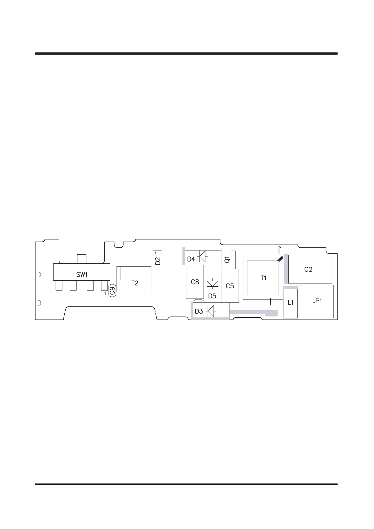
5) FLASH_TOP …………………………………………………………………………………………………51
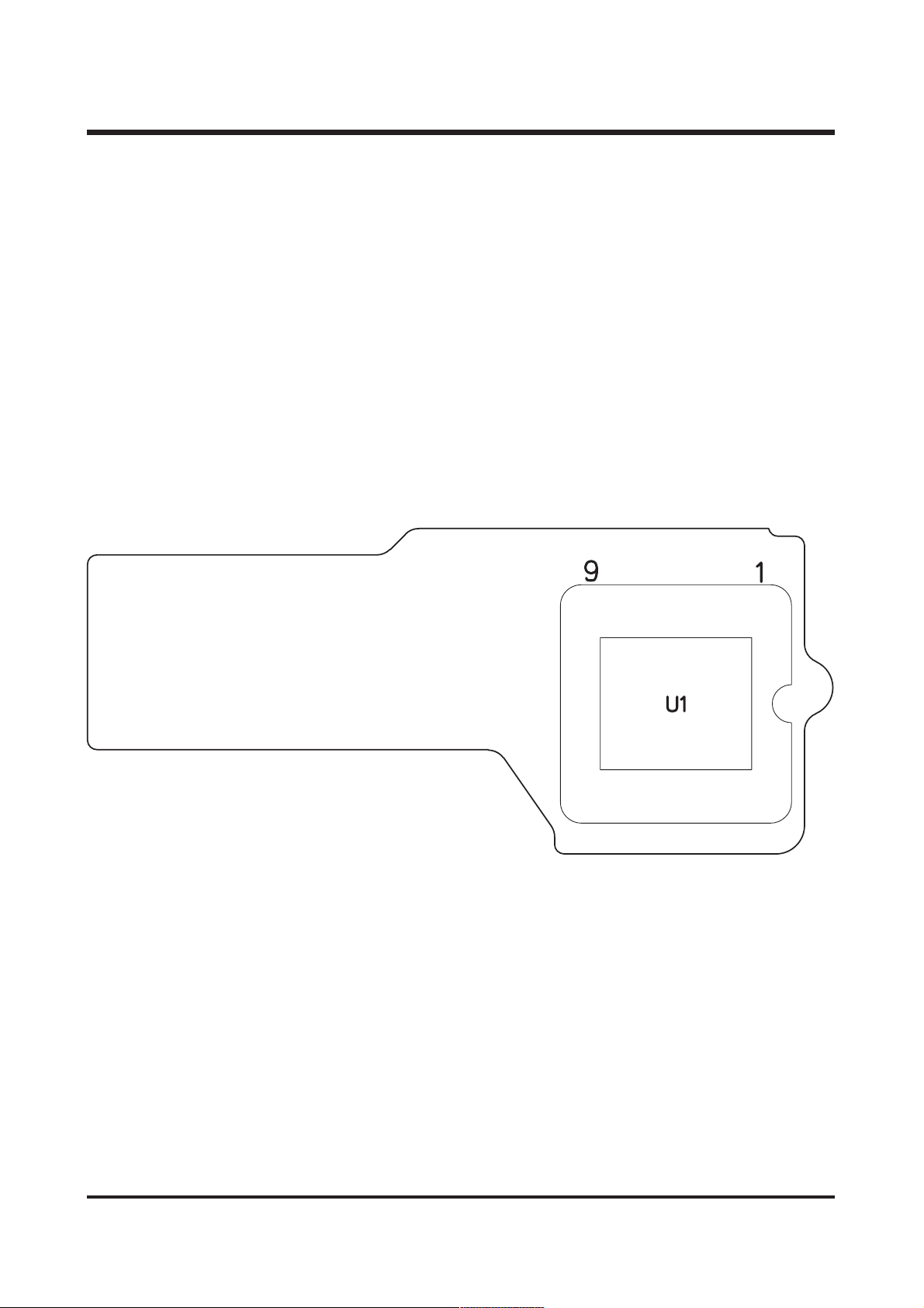
6) FLASH_BOTTOM ……………………………………………………………………………………………52
7) CCD_TOP ……………………………………………………………………………………………………53
8) CCD_BOTTOM ………………………………………………………………………………………………54
9) USB_TOP ……………………………………………………………………………………………………55
10) USB_BOTTOM ………………………………………………………………………………………………56
ⅥⅥ.. CCIIRRCCUUIITT DDIIAAGGRRAAMM
1. BLOCK DIAGRAM…………………………………………………………………………………………………57
2. CIRCUIT DIAGRAM
1) TOP VIEW ……………………………………………………………………………………………………58
2) SPCA536 DSP …………………………………………………………………………………………………59
3) IMAGE SENSOR-PERIPHERIC CIRCUIT ……………………………………………………………………60
3-1) IMAGE SENSOR-PERIPHERIC CIRCUIT …………………………………………………………………61
3-2) IMAGE SENSOR-PERIPHERIC CIRCUIT …………………………………………………………………62
4) TRAP/EEPROM ………………………………………………………………………………………………63
5) TFT LCD ………………………………………………………………………………………………………64
6) USB 1.1/MIC/TVOUT/BUZZE ………………………………………………………………………………65
7) POWER MODULE-AT 1388 …………………………………………………………………………………66
8) POWER SOURCE/RESET/LED ………………………………………………………………………………67
9) INTERFACE IO…………………………………………………………………………………………………68
10) IMAGE SENSOR FPC-MN39620 ……………………………………………………………………………69
11) STROBE FLASH ……………………………………………………………………………………………70
12) USB/VO/AO/HEADPHONE/MIC/SPK ………………………………………………………………………71
13) KEY/SD CON ………………………………………………………………………………………………72
Page 2

3
ⅦⅦ.. TTRROOUUBBLLEESSHHOOOOTTIINNGG
1. Check List for Repairing ………………………………………………………………………………………73
2. Main Troubleshooting ……………………………………………………………………………………………74
3. How to DISASSEMBLY …………………………………………………………………………………………80
Page 3
4
ⅠⅠ.. SSPPEECCIIFFIICCAATTIIOONN
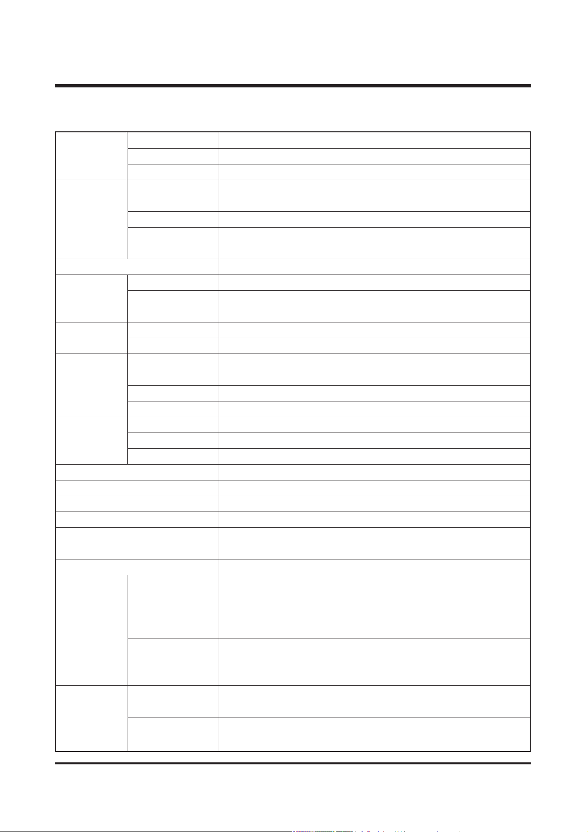
11.. CCAAMMEERRAA SSPPEECCIIFFIICCAATTIIOONN
Type 1/2.5" CCD
Effective Pixels Approx. 5.0 Mega-pixel
Total Pixels Approx. 5.2 Mega-pixel
Lens f=5.8mm
(35mm film equivalent:35mm)
F No. F3.2 / F7.0
Still Image mode: 1.0X ~ 5.0X
Play mode: 1.0X~8.0X (depends on Image size)
LCD Monitor 2.0" colour TFT LCD
Type TTL Auto Focus
Normal: 0.6m~infinity
Macro: 6 cm ~ 60cm
Type Mechanical and Electronic shutter
Speed 2 ~ 1/1000 sec. (8 ~ 1/1000sec.in Night Mode)
Programmed AE
Metering: Multi, Spot
Compensation ±2EV (0.5EV steps)
ISO Equivalent Auto, 100, 200, 400
Modes Auto, Auto & Red - eye reduction, Fill-in flash, Slow sync, Flash Off
Range 0.3m ~ 3.0m
Recharging Time Approx. 3 ~ 5 sec.
Sharpness Soft, Normal, Vivid
Effect Normal, B&W, Sepia, RGB
White Balance Auto, Daylight, Cloudy, Sunset, Fluorescent(H), Fluorescent(L),Tungsten, Custom
Photo Frame 9 Frames
Voice Recording (max. 1 hour)
Voice Memo on Still Image (max. 10.sec)
Date Imprinting Off , Date, Date & Time (User selectable)
Mode: Auto, Program, Scene
* Scene : Night, Portrait, Landscape, Text, Fireworks
Shooting: Single, continuous
Self-timer: 2 sec., 10 sec, Double Self Timer (10 / 2sec.)
With audio (recording time: memory capacity dependent)
Size: 640 x 480, 320 x 240
Frame rate: 24fps, 15fps * no digital zoom in movie clip
Internal memory: 16MB flash memory
External memory: SD card /MMC (Up to 512MB Guaranteed)
Still Image: JPEG (DCF), EXIF 2.2, DPOF 1.1, PictBridge 1.0
Movie Clip: AVI (MJPEG) Audio: WAV
Image Sensor
Lens
Digital Zoom
Range
Focal Length
Still Image
Movie Clip
Media
File Format
Control
Focusing
Shutter
Exposure
Flash
Shooting
Voice Recording
Storage
Page 4
5
Ⅰ. SPECIFICATION
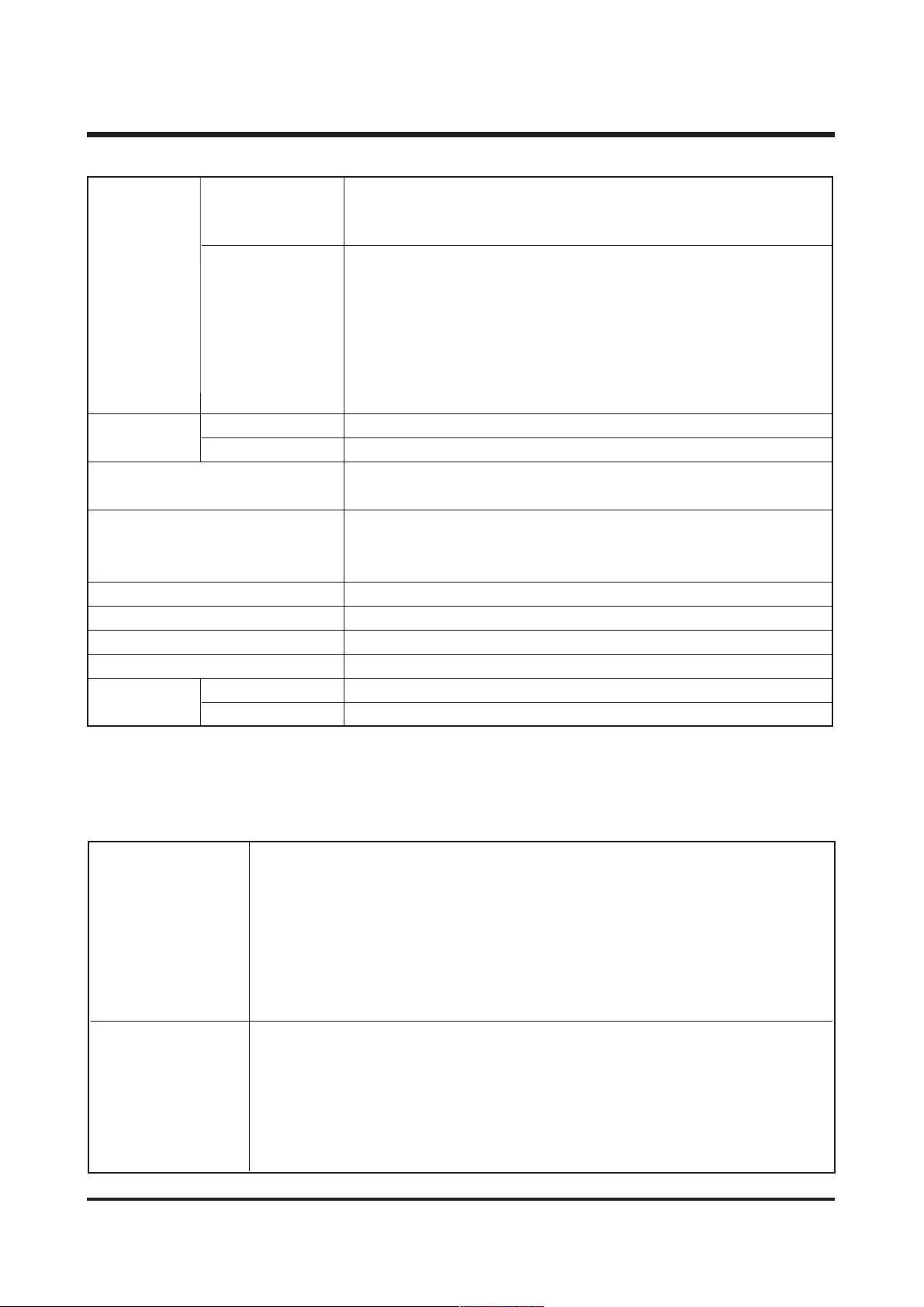
2560 : 2560x1920 pixels, 2048 : 2048x1536 pixels
1600 : 1600x1200 pixels, 1024 : 1024x768 pixels,
640 : 640x480 pixels
2560 : Super fine (9) / Fine (18) / Normal (29)
2048: Super fine (10 ) / Fine (24) / Normal (38)
1600: Super fine (16 ) / Fine (36) / Normal (58)
1024: Super fine (36) / Fine (67) / Normal (117)
640: Super fine (72) / Fine (121) / Normal (214)
* These figures are measured under Samsung’s standard conditions and
may vary depending on shooting conditions and camera settings.
Type Single image / Thumbnails / Slide show/ Movie Clip
Editing Rotation, Trimming, Resizing
Digital output connector: USB 1.1
Video output: NTSC, PAL (User selectable)
Primary battery: 3V Lithium battery (CP1)
Rechargeable battery: 3.7V Li-ion battery (SLB-1137)Charger : SBC-L3
Included battery may vary depending on sales region.
Dimensions (WxHxD) 97 x 52 x 23 mm
Weight Approx. 110g (without batteries and card)
Operating Temperature 0 ~ 40 °C
Operating Humidity 5 ~ 85%
Camera Driver Storage Driver (Windows98/98SE/2000/ME/XP, Mac OS 9.0 ~10.2 )
Application Arcsoft PhotoImpression, Digimax Viewer, Digimax Reader
Capacity
(16MB)
Image Size
Storage
Power Source
이미지재생
Software
Interface
22.. SSYYSSTTEEMM RREEQQUUIIRREEMMEENNTTSS
PC with processor better than MMX Pentium 233MHz (XP : Pentium II 300MHz)
Windows 98/98SE/2000/ME/XP
For Windows Minimum 32MB RAM (XP : 128MB)
140MB of available hard-disk space, USB port, CD-ROM drive,
800×600 pixels, 16-bit colour display compatible monitor
(24-bit color display recommended)
Power Mac G3 or later
Mac OS 9.0 ~ 10.2
For Macintosh Minimum 64MB RAM
110MB of available hard-disk space, USB port, CD-ROM drive,
QuickTime 4.0 or later for Movie Clip
Page 5
6
Ⅰ. SPECIFICATION
②
③
④
⑤
⑥
⑦
⑧
⑪
⑨
⑩
⑫
⑬
⑭
⑮
⒃
⒔
⒕
⒗
⒖
①
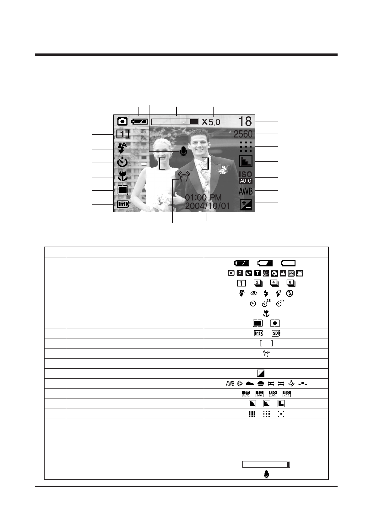
33.. TTFFTT LLCCDD PPAANNEELL MMAARRKK
■ Recording mode
No. Description Icons
1 Battery
2 Recording mode
3 Continuous shot
4 Flash
5 Self-timer
6 Macro
7 Metering
8 Card inserted indicator
9 Auto focus frame
10 camera shake warning
11 Date/Tme 2004/10/01 01:00 PM
12 Exposure conpensation
LLTT
13 White Balance
14 ISO
15 Sharpness
16 Image quality
17 Image Size 2560, 2048, 1600, 1024, 640
Number of available shots remaining 18
Remaining time(Movie dip/Voice recording) 00:01:25 / 00:24:52
19 Digital zoom rate X5.0
20 Digital zoom bar
21 Voice memo
18
Page 6
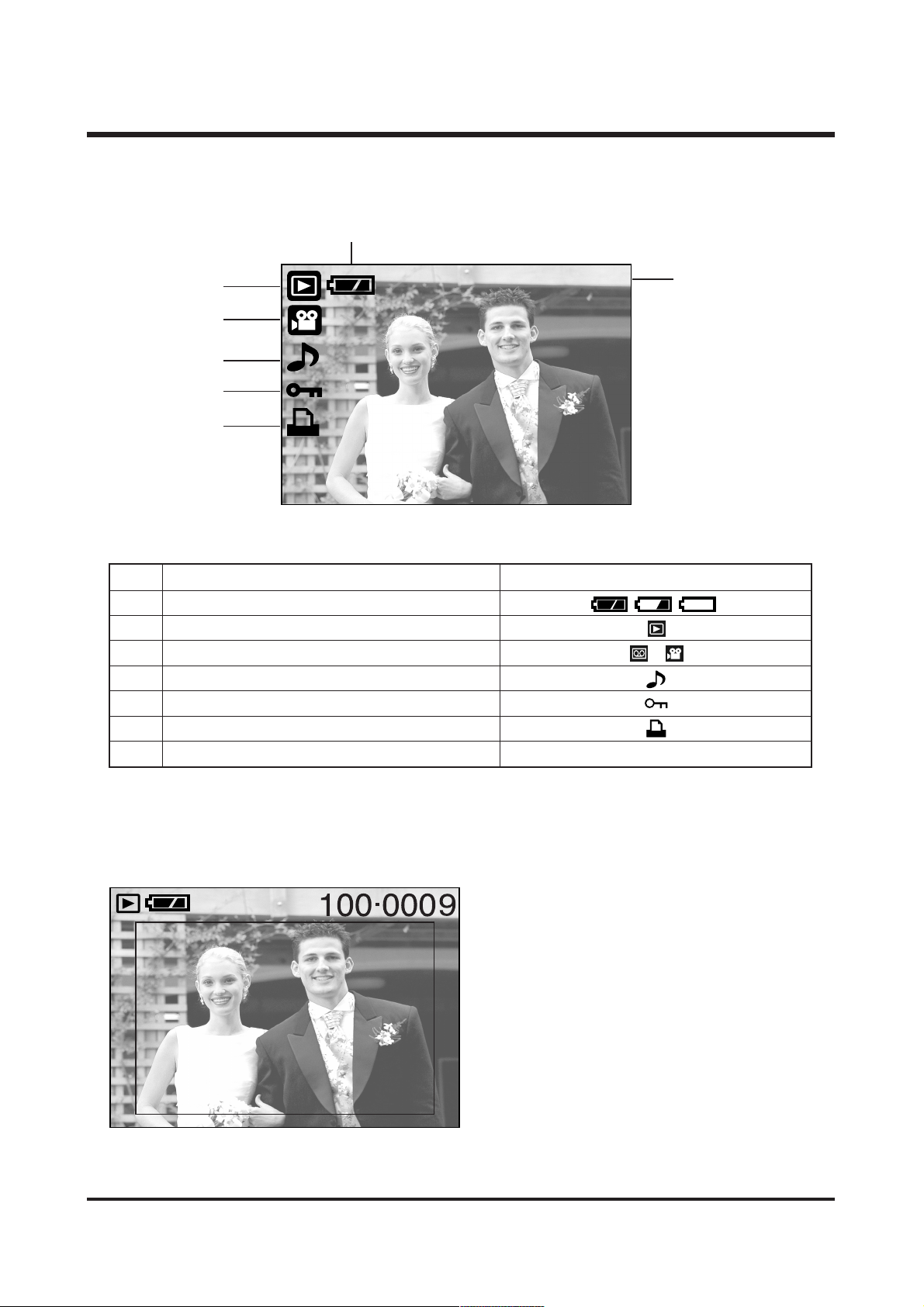
NO. Description Icons
1 Battery
2 Play mode
3 File Type
4 Voice memo
5 Protect indicator
6 DPOF indicator
7 Stored image number 100-0009
7
Ⅰ. SPECIFICATION
②
③
④
⑤
⑥
⑦
①
■ Play mode
100-0009
SIZE : 2560X1920 Size
AV : F3.2 Aperture value
TV : 1/18 Shutter speed
FLASH : OFF Whether or not
the flash is used.
DATE : 2004/10/01 Recording date
SSIIZZEE :: 22556600XX11992200
AAVV :: FF33..22
TTVV :: 11//1188
FFLLAASSHH :: OOFFFF
DDAATTEE :: 22000044//1100//0011
Page 7
8
Ⅰ. SPECIFICATION
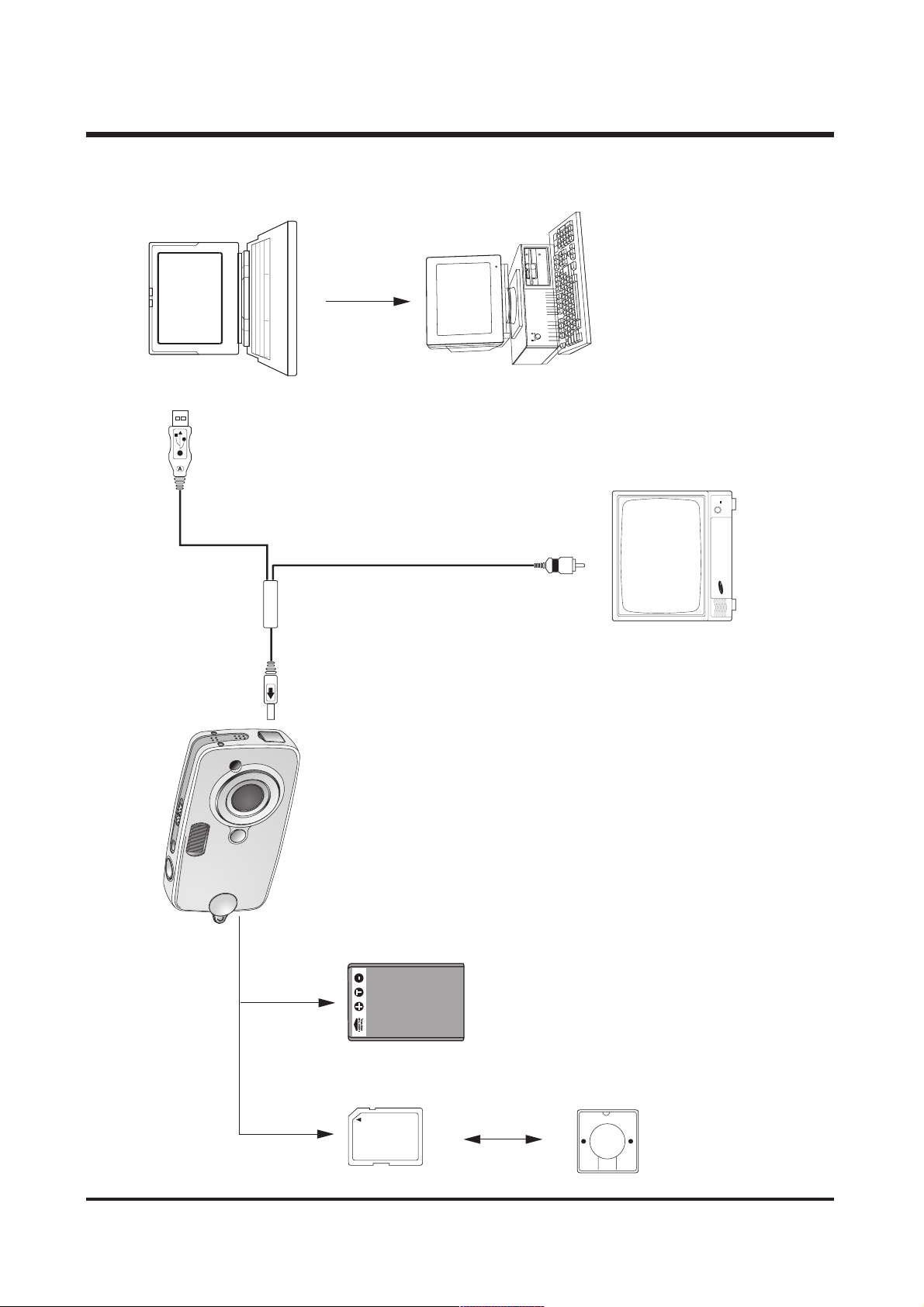
44.. CCOONNNNEECCTTIIOONN DDIIAAGGRRAAMM
USB Cable
Lap top
IBM / MAC
Video Cable
TV Monitor
SLB-1037
SD Card
Card Reader
Page 8
9
Ⅰ. SPECIFICATION
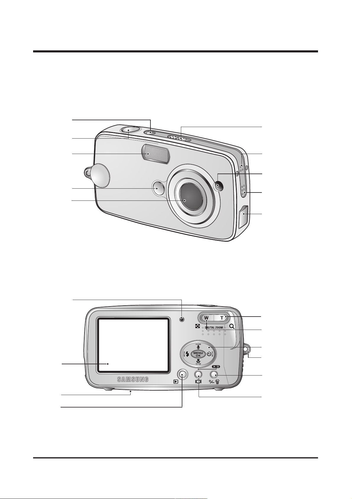
55.. IIDDEENNTTIIFFIICCAATTIIOONN OOFF FFEEAATTUURREESS
Shutter button
Flash
Lens
USB connection port/
Video connection
terminal
Mode switch
Microphone
Self-timer lamp/
Auto Focus lamp
Power button
Mirror for
self portrait
Speaker
LCD monitor
Camera status lamp
Strap eyelet
Zoom T button (Digital zoom)
Zoom W button (Thumbnail)
Play mode button
Tripod socket
LCD button
+/-,
DELETE
button
5-function button
Page 9
10
Ⅰ. SPECIFICATION
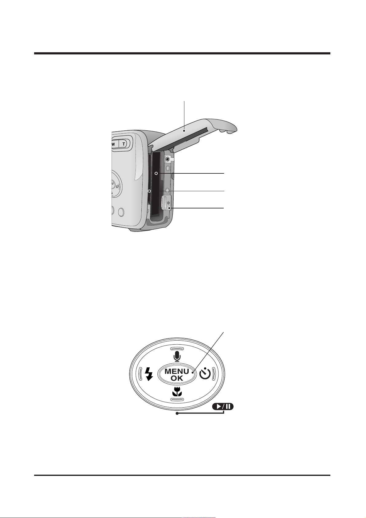
FLASH/ LEFT
button
MENU/ OK
button
MACRO/ DOWN button
PLAY&PAUSE button
SELF-TIMER/
RIGHT button
Voice memo/ UP button
Battery holder
Memory card slot
Battery chamber
Battery chamber cover
Page 10
11
ⅡⅡ.. IINNSSTTAALLLLAATTIIOONN
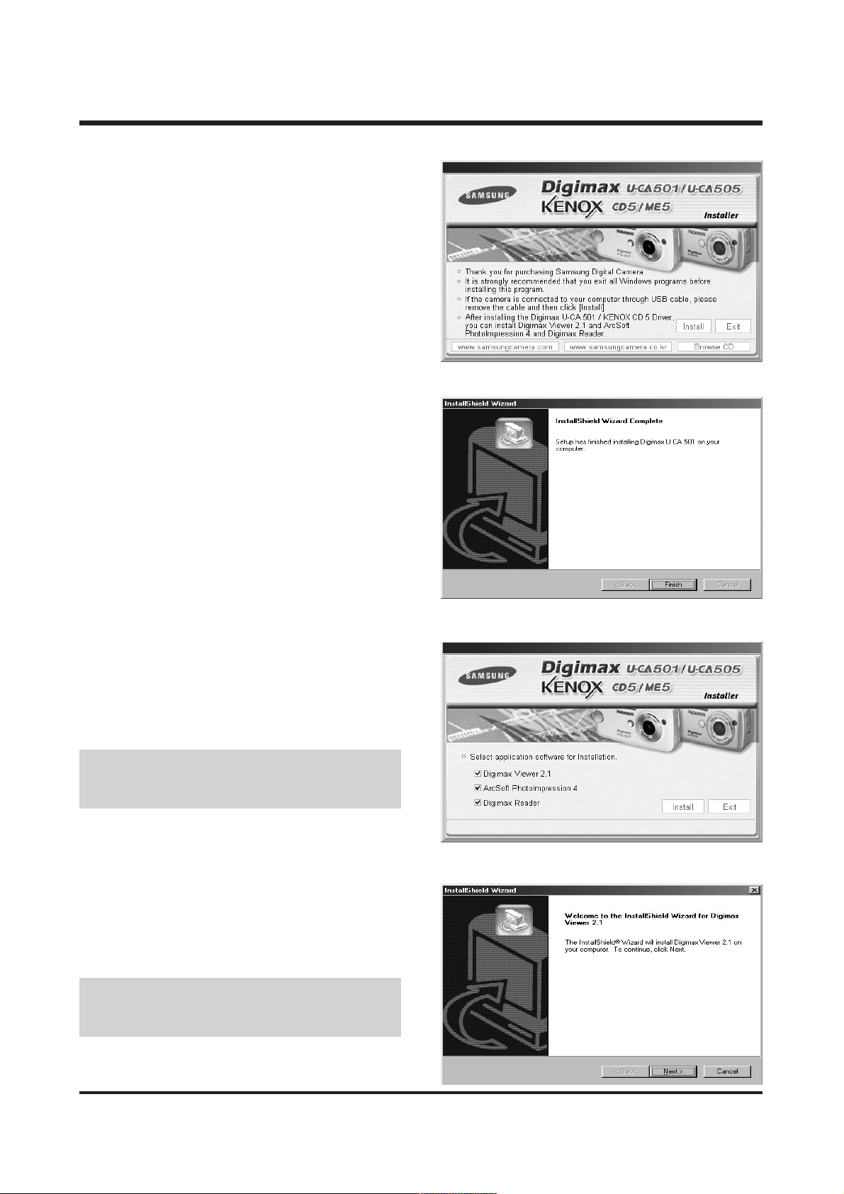
1. Click the [Install] menu in the Autorun frame.
The camera driver is installed automatically.
2. Camera driver installation is complete.
Click the [Finish] button.
● If you select [Exit] at the step 3, the appli-
cation program installation will be cancelled.
● If you select [Cancel] at step 4, a window for
installing PhotoImpression will be displayed.
3. A window for which you can select application
software will be displayed. Select the application program and click the [Install] button.
Refer to page 89 for more information about
the application program.
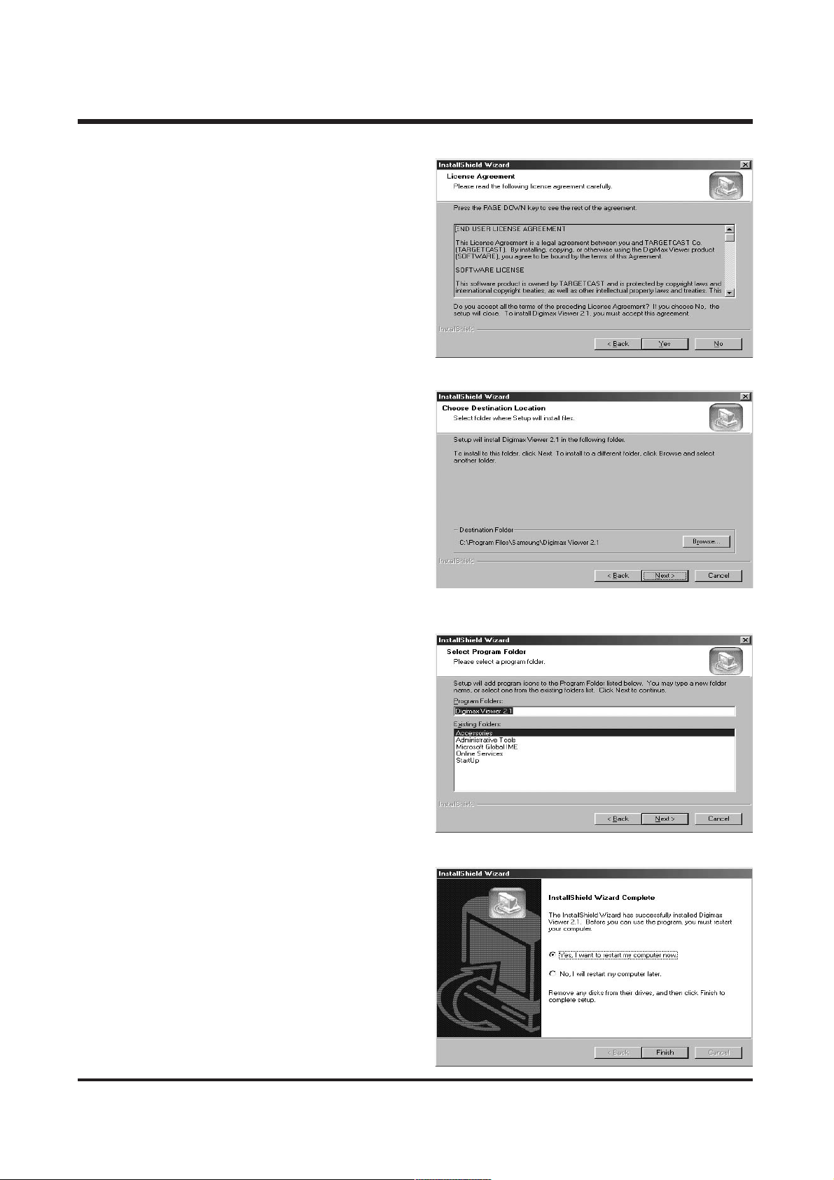
4. Install Digimax Viewer.
Click [Next >] button.
Page 11
12
ⅡⅡ
.. IINNSSTTAALLLLAATTIIOONN
5. The Software License Agreement window will
be displayed. If you agree to this, click
[Yes], the window will then move to the
next step.
If you disagree, click [No] and the installation program will be canceled.
6. A destination selection window will open.
Click [Next >]. To copy to the files to
another folder, click [Browse..] and choose
a folder you want.
8. Digimax Viewer installation is successfully completed. Click the [Finish] button to install
PhotoImpression. The system will not reboot
even the [Yes, I want to restart the computer
now] option is selected.
* The frame 8 may not appear according to
the system requirements.
7. A window will open, asking you to choose a
folder to which program icons will be added.
Click [Next >] button. If you want to add the
program icons to a different folder, choose
another folder, and then click [Next >] button.
Page 12
13
ⅡⅡ
.. IINNSSTTAALLLLAATTIIOONN
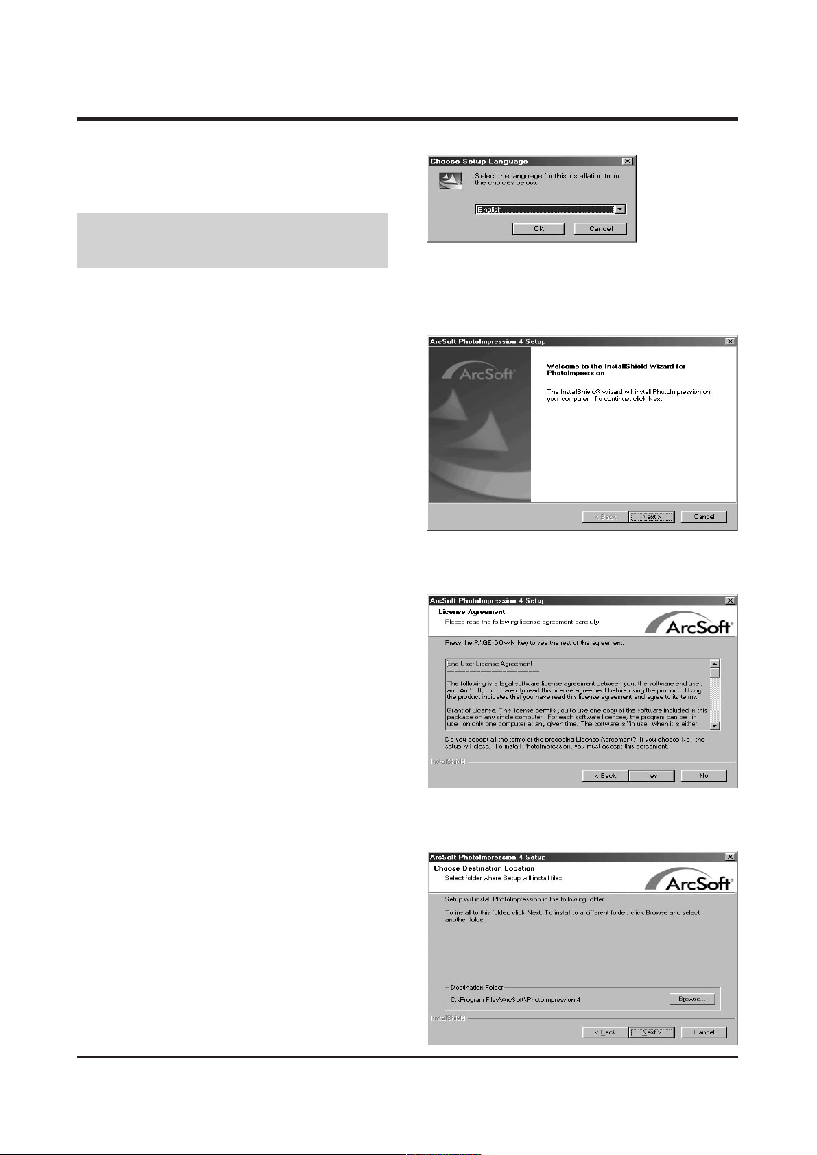
9. The PhotoImpression installation window will be
displayed as shown alongside. Click the [OK]
button.
● If you select [Cancel] at step 9, a window for
installing Digimax Reader will be displayed.
10. A Welcome window will be displayed.
Click the [Next >] button.
12. A destination selection window will open. Click
[Next >]. To copy to the files to another
folder, click [Browse...] and choose a folder
you want.
11. The Software License Agreement window will
be displayed. If you agree to this, click [Yes],
the window will then move to the next step.
If you disagree, click [No] and the installation
program will be canceled.
Page 13
14
ⅡⅡ
.. IINNSSTTAALLLLAATTIIOONN
16. Digimax Reader를 설치합니다.
[설치하기]를 클릭하십시오.
- [설명서]를 클릭하면 Digimax Reader의 간
단한 설명이 나타납니다.
- [종료]를 선택하면 Digimax Reader
설치를 종료하고 컴퓨터 재시작을 위한 완료
창이 나타납니다.
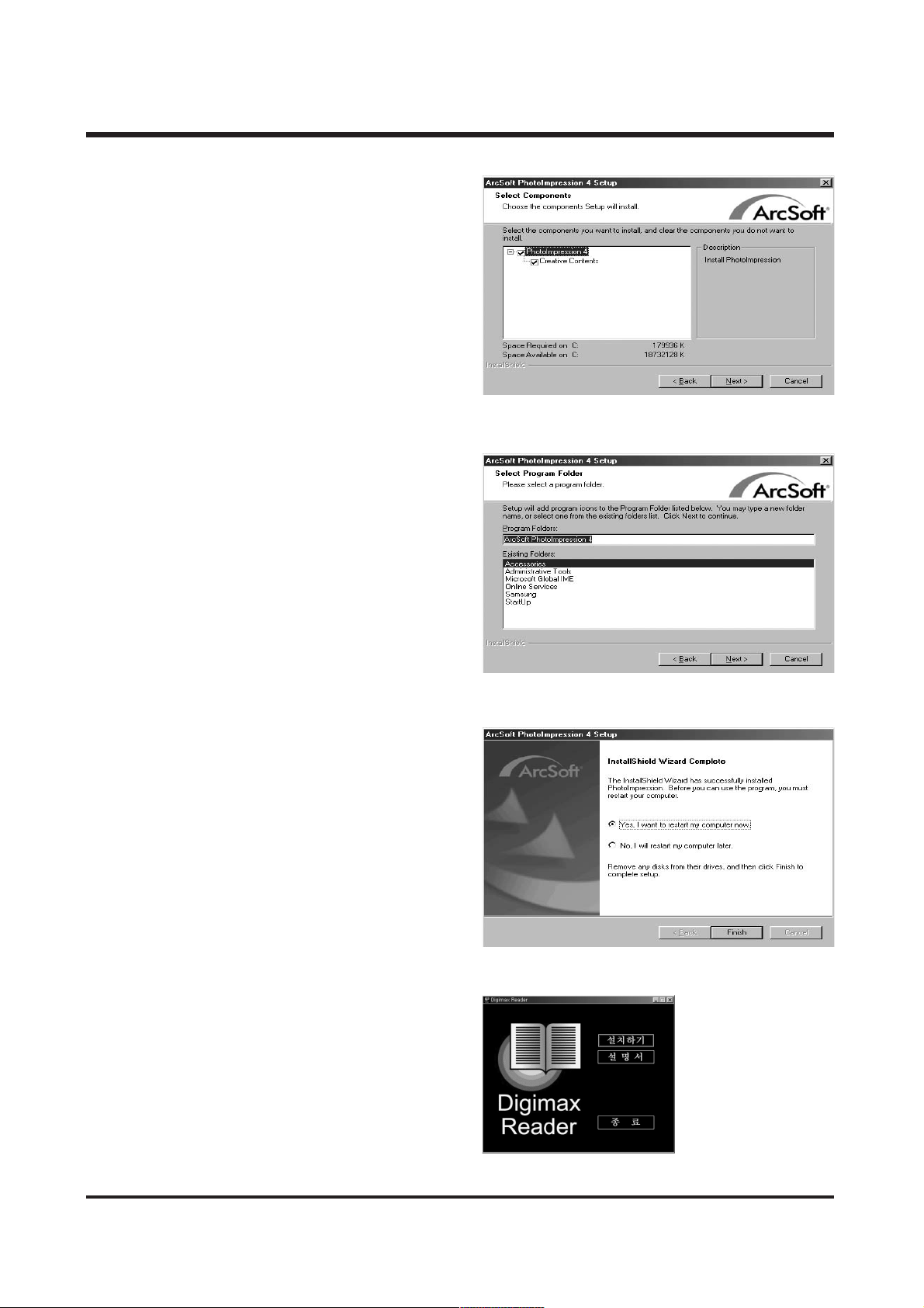
13. The [Select Components] window will appear.
Click [Next >] button.
14. A window will open, asking you to choose a
folder to which program icons will be added.
Click [Next >] button. If you want to add the
program icons to a different folder, choose
another folder, and then click [Next >] button.
15. PhotoImpression installation is successfully
completed. Click the [Finish] button to install
Digimax Reader.
* The system will not reboot even the [Yes, I
want to restart the computer now] option is
selected.
* The frame 15 may not appear according to
the system requirements.
Page 14
15
ⅡⅡ
.. IINNSSTTAALLLLAATTIIOONN
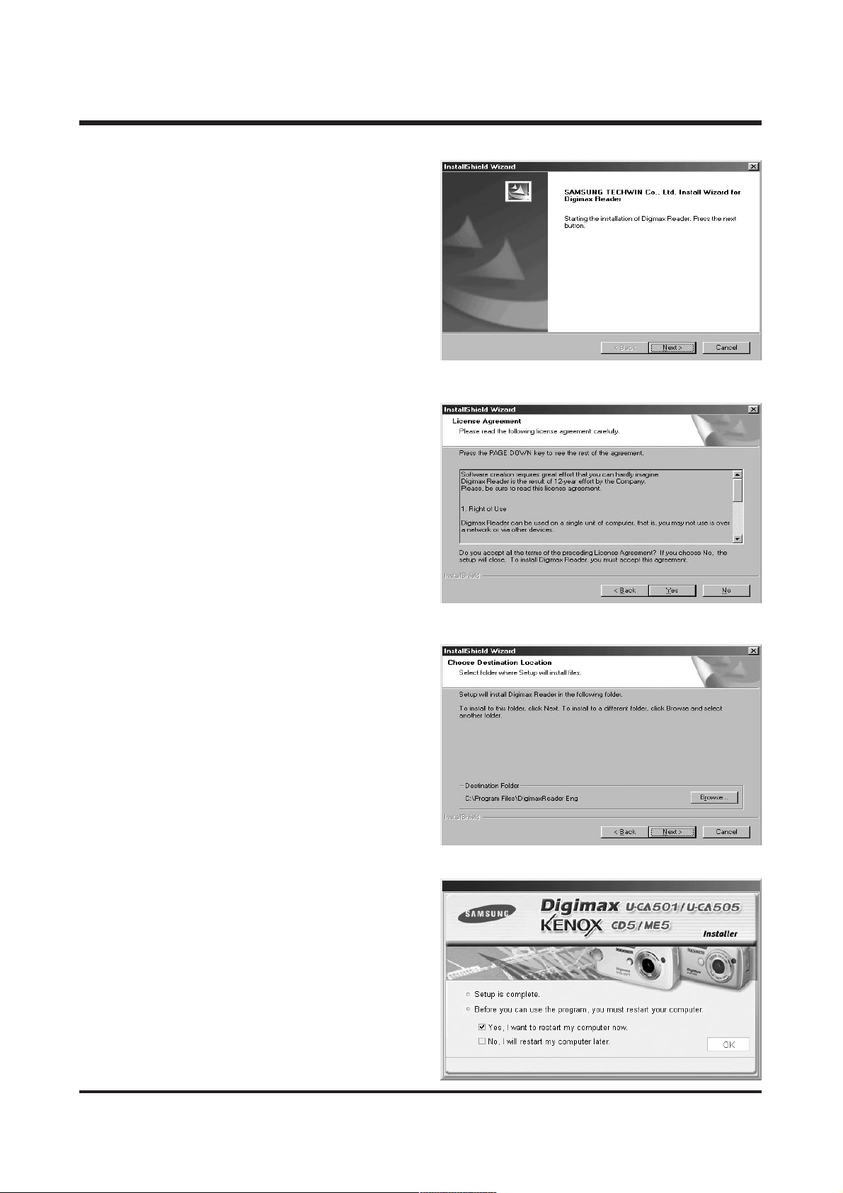
17. A window will open. Click the [Next(N)>]
button.
18. The Software License Agreement window will
be displayed. If you agree to this, click
[Yes], the window will then move to the next
step.
If you disagree, click [No] and the installation program will be canceled.
19. A destination selection window will open.
Click [Next >]. To copy to the files to another folder, click [Browse...] and choose a
folder you want.
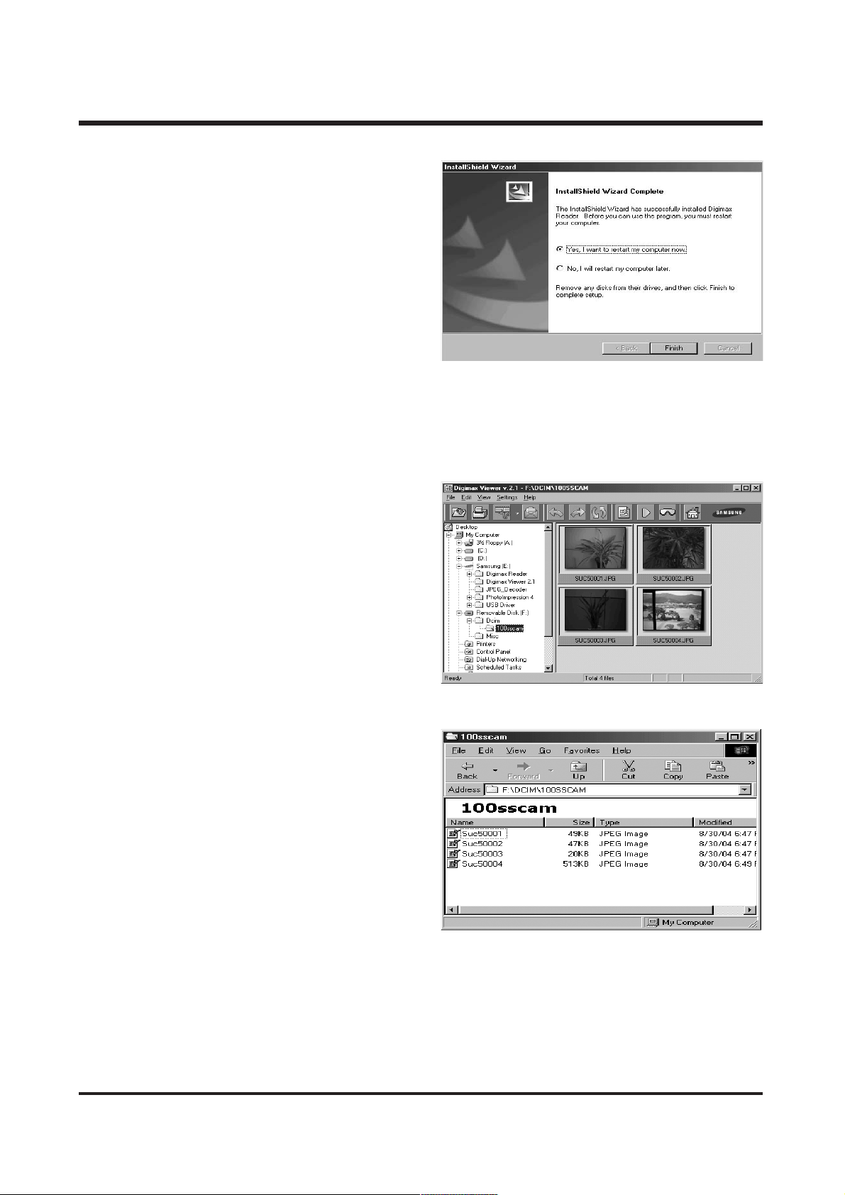
20. Installation is complete. To apply changes,
you must restart the computer. Select [Yes, I
want to restart my computer now], and then
click [OK].
Page 15
16
ⅡⅡ
.. IINNSSTTAALLLLAATTIIOONN
* The frame 20 may be displayed according to
the system requirements. Click the [Finish]
button to restart the computer.
21. After restarting the computer, connect the PC to the camera with the USB cable.
22. Turn the camera power on. [Found New
Hardware Wizard] will open and the computer will recognise the camera.
* If you have ever installed an image viewer
program or your OS is Windows XP, an
image viewer program will open. If the image
viewer program opens, the camera driver
was setup successfully.
23. If you can see [Removable Disk] under [My
computer], the camera driver installation was
successful. Now you can transfer image files
from the camera to PC via the USB cable.
Page 16

17
ⅡⅡ
.. IINNSSTTAALLLLAATTIIOONN
● If you have installed the camera driver, [Found New Hardware Wizard] may not open.
● On a Windows 98 or 98 SE system, the Found New Hardware Wizard dialog box opens and a window
asking you to select a driver file may appear. In this case, specify "USB Driver" in the CD supplied.
● Before connecting the camera to the PC, You should first install the camera driver.
● After installing the camera driver, you have to restart your PC.
● If you connect the camera to the PC before installing the camera driver, the [Found New Hardware
Wizard] will open.
In this case, cancel the [Found New Hardware Wizard] and disconnect the camera. Install the camera
driver and connect the camera to the PC again.
● Should the computer not find the camera driver after installation, please try one or more of the fol-
lowing measures.
1. Delete the camera driver, and re-install the driver.
2. Refer to FAQ to check for a possible solution to the problem.
3. If your PC’s central processing unit is VIA chip (This is shown in the USB Host Controller), download
the patch file from the Samsung Camera web page. (http://www.samsungcamera.com)
Page 17
18
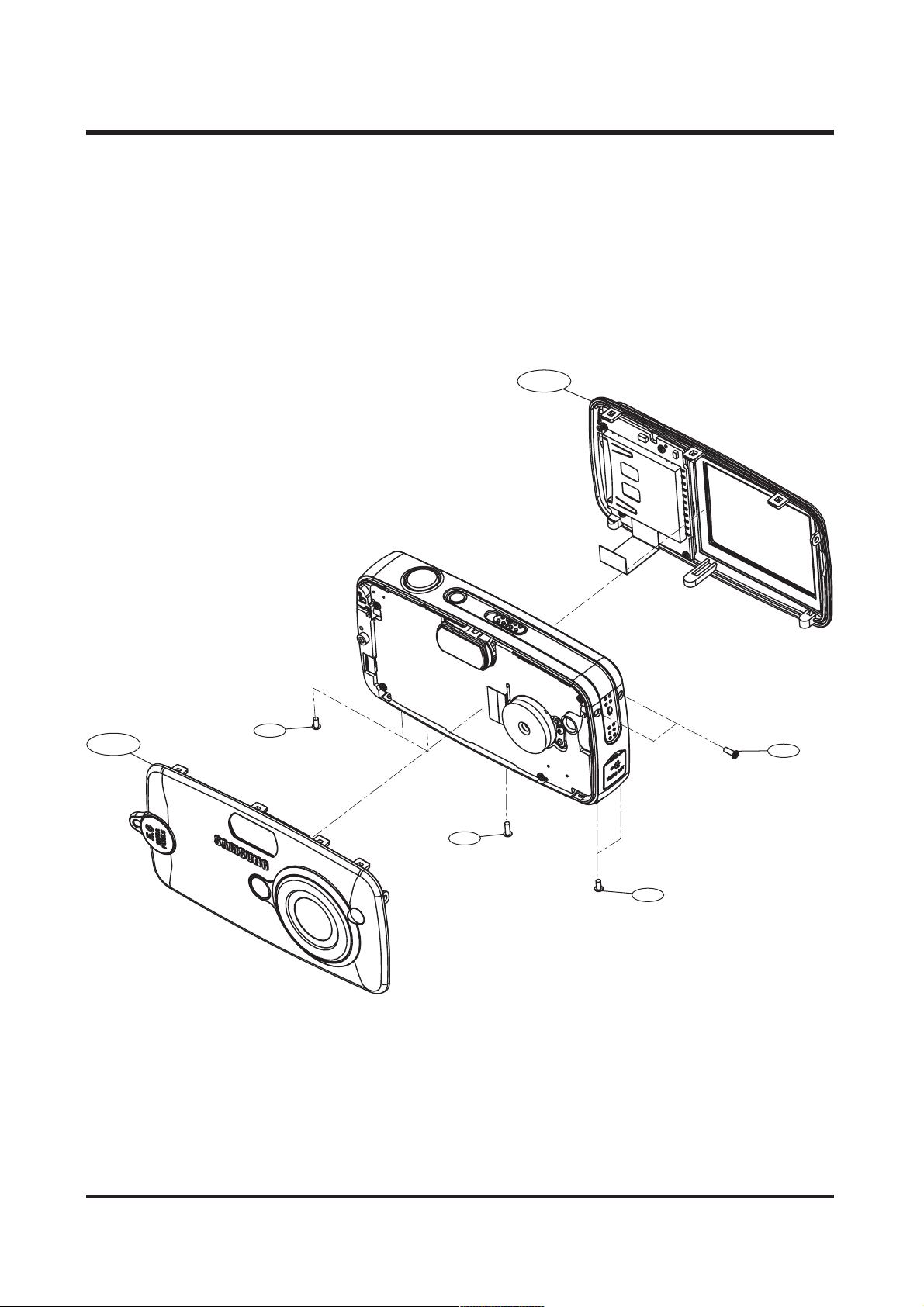
ⅢⅢ.. EEXXPPLLOODDEEDD VVIIEEWWSS AANNDD PPAARRTTSS LLIISSTT
1. MAIN ASSEMBLY
1818
1-2
1-1
1-4
1-3
1-3
1-4
Page 18
19
Ⅲ. EXPLODED VIEWS AND PARTS LIST
1919
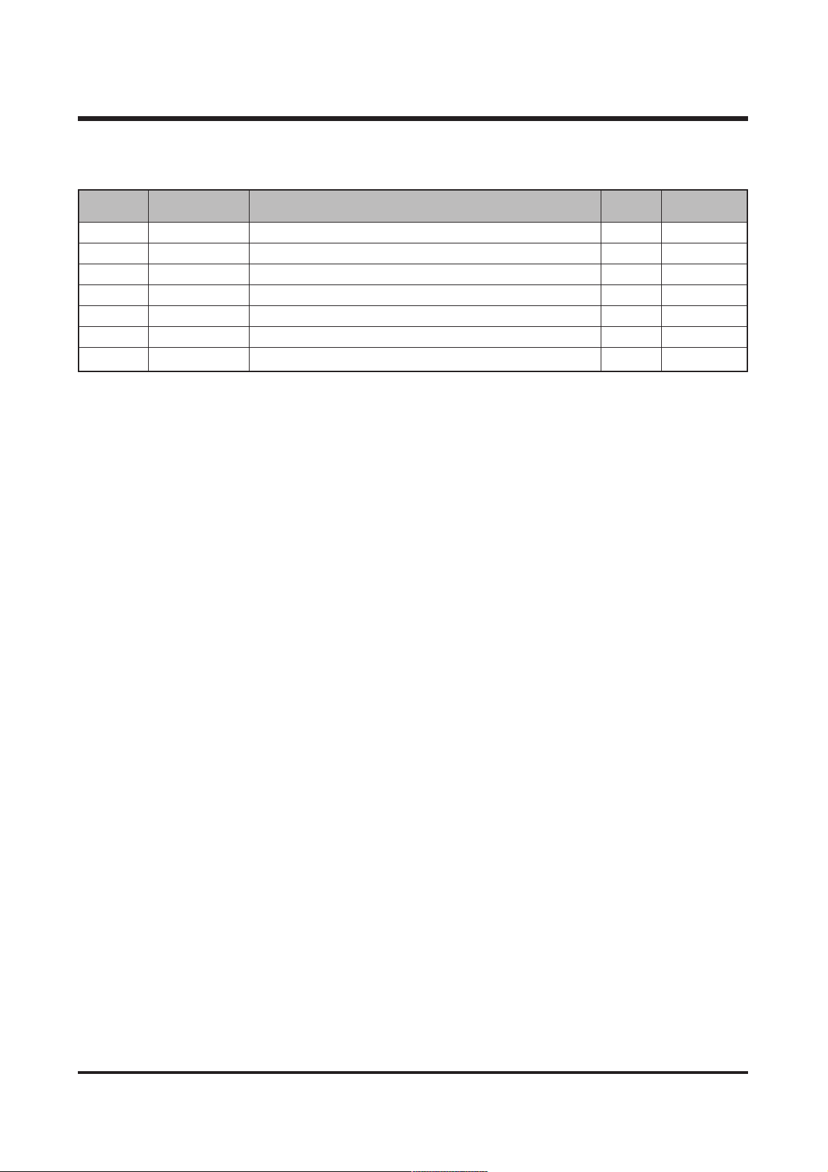
FFiigg..NNoo.. PPaarrttss NNoo.. PPaarrttss NNaammee QQ''ttyy RReemmaarrkkss
1-1 Q9007967501A FRONT COVER ASS'Y-U CA 501 1
Q9007967601A FRONT COVER ASS'Y-U CA 505 1
Q9007967701A FRONT COVER ASS'Y-KENOX CD 5 1
Q9007220901A FRONT COVER ASS'Y-KENOX ME 5 1
1-2 Q9007221001A BACK COVER ASS'Y 1
1-3 Q6002024201A TAPPING SCREW 3
1-4 Q6002024301A TAPPING SCREW 4
▶▶
PARTS LIST
Page 19
20
Ⅲ. EXPLODED VIEWS AND PARTS LIST
20
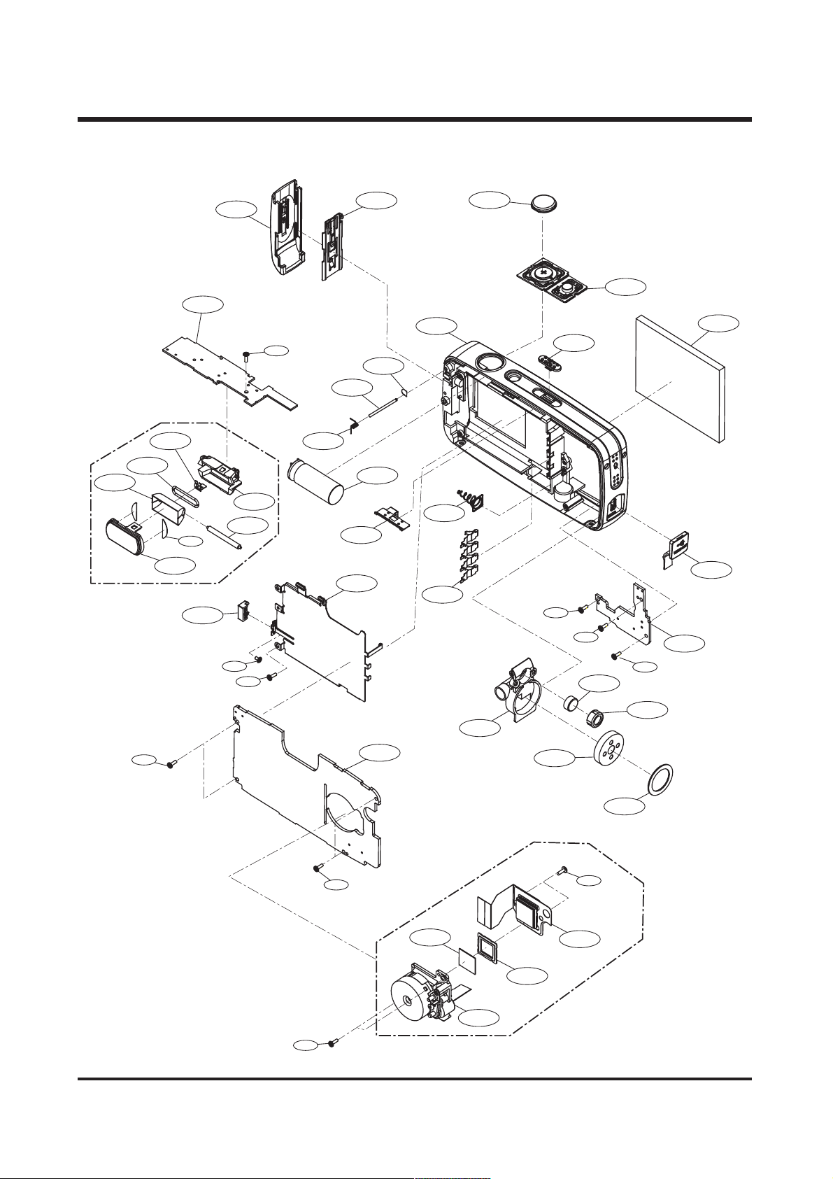
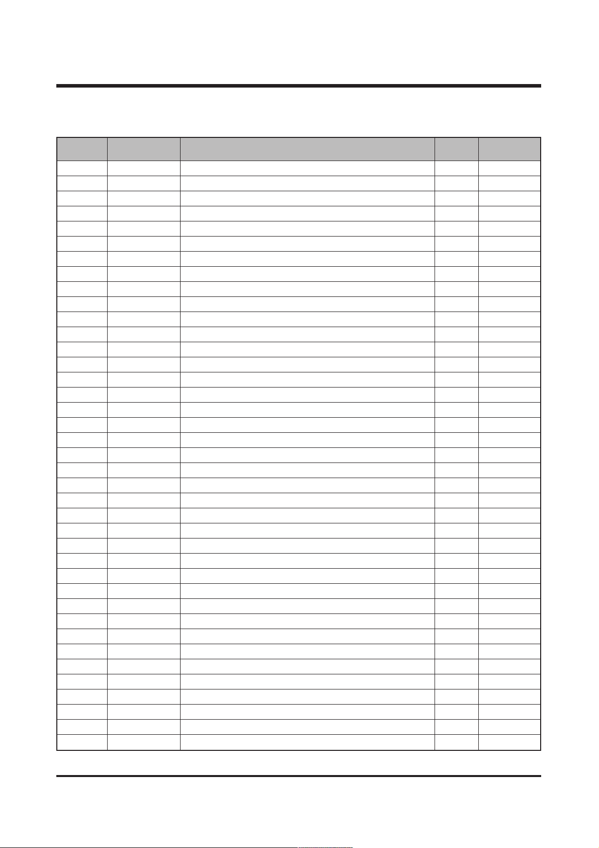
2. BODY ASSEMBLY
2-26
2-24
2-25
2-29
2-28
2-16
2-33
2-4
2-35
2-17
2-27
2-12
2-12
2-6
2-7
2-13
2-32
2-5
2-8
2-18
2-3
2-31
2-30
2-9
2-12
2-2
2-15
2-14
2-1
2-10
2-11
2-12
2-22
2-12
2-12
2-12
2-34
2-37
2-23
2-19
2-20
2-21
2-12
2-39
2-38
2-36
Page 20
21
Ⅲ. EXPLODED VIEWS AND PARTS LIST
21
FFiigg..NNoo.. PPaarrttss NNoo.. PPaarrttss NNaammee QQ''ttyy RReemmaarrkkss
2-1 Q0704010801A TFT LCD 1
2-2 Q7204020101A MODE BUTTON 1
2-3 Q7217340801A MID COVER 1
2-4 Q7204020701A BATTERY COVER 1
2-5 Q7101000101A BATTERY CONTACT LOWER 1
2-6 Q6107061301A SPRING BATTERY COVER 1
2-7 Q7411116601A BATTERY SHAFT 1
2-8 Q7102000101A SCREW MYLAR 1
2-9 Q7217341501A RELEASE BUTTON 1
2-10 Q7309044701A JACK COVER 1
2-11 Q9008080901A USB SMD 1
2-12 Q6002024401A TAPPING SCREW 12
2-13 Q7204019701A MODE BUTTON METAL 1
2-14 Q7307005701A POWER BUTTON 1
2-15 Q6002024501A TAPPING SCREW 1
2-16 Q9008081001A FL SMD 1
2-17 Q7204019801A VR HOLDER 1
2-18 Q7204019901A PHOTO FLASH CAP 1
2-19 Q7204020001A MIC SPK HOLDER 1
2-20 Q3001000101A SPEAKER 1
2-21 Q7204020201A SPEAKER SPONGE 1
2-22 Q3003000301A MICROPHONE 1
2-23 Q7204020301A MIC RUB RING 1
2-24 Q7309044801A FLASH RUBBER 1
2-25 Q7204020401A TRIGGER CONTACT 1
2-26 Q7014005101A FLASH REFLECTOR 1
2-27 Q0611004101A FLASH TUBE BGDC 1
2-28 Q7204020501A VF MYLAR 2
2-29 Q7217340701A FLASH COVER ACRLY 1
2-30 Q7011051101A BATTER CONTACT UPPER-PT 4
2-31 Q6107061201A BATTERY PUSH SPRING 1
2-32 Q7017044601A BATTERY HOLDER SHEET 1
2-33 Q7204020601A BATTERY LOCK 1
2-34 Q9008081101A MA DIP 1
2-35 Q6002024601A TAPPING SCREW 1
2-36 Q9002134301A BARREL ASS'Y 1
2-37 Q2904002801A CCD GLASS 1
2-38 Q7309045001A CCD RUBBER 1
2-39 Q9002134401A CCD F PCB ASS'Y 1
▶▶
PARTS LIST
Page 21
22
Ⅲ. EXPLODED VIEWS AND PARTS LIST
22
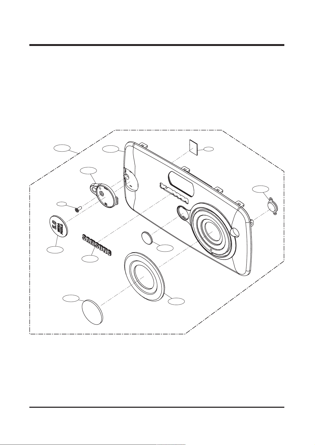
3. FRONT COVER ASSEMBLY
3-10
3-1
3-11
3-9
3-5
3-6
3-3
3-2
3-4
3-7
3-8
Page 22
23
Ⅲ. EXPLODED VIEWS AND PARTS LIST
23
FFiigg..NNoo.. PPaarrttss NNoo.. PPaarrttss NNaammee QQ''ttyy RReemmaarrkkss
3-1 Q9007967501A FRONT COVER ASS'Y-U CA 501 1
Q9007967601A FRONT COVER ASS'Y-U CA 505 1
Q9007967701A FRONT COVER ASS'Y-KENOX CD 5 1
Q9007220901A FRONT COVER ASS'Y-KENOX ME 5 1
3-2 Q7102000201A STRAP RING MYLAR 1
3-3 Q7217341301A FRONT COVER-U CA 501 1
Q7217341401A FRONT COVER-U CA 505 1
Q7204021301A FRONT COVER-KENOX CD 5 1
Q7204021401A FRONT COVER-KENOX ME 5 1
3-4 Q7204021501A FRONT LED GUIDE 1
3-5 Q7204021601A STRAP RING 1
3-6 Q7217303501A SAMSUNG PLATE 1
3-7 Q7217341201A MIRROR 1
3-8 Q7117009801A LENS RING 1
3-9 Q7217341601A LENS COVER 1
3-10 Q7204021201A STRAP RING DECORATION 1
3-11 Q6002024701A TAPPING SCREW 1
▶▶
PARTS LIST
Page 23
24
Ⅲ. EXPLODED VIEWS AND PARTS LIST
24
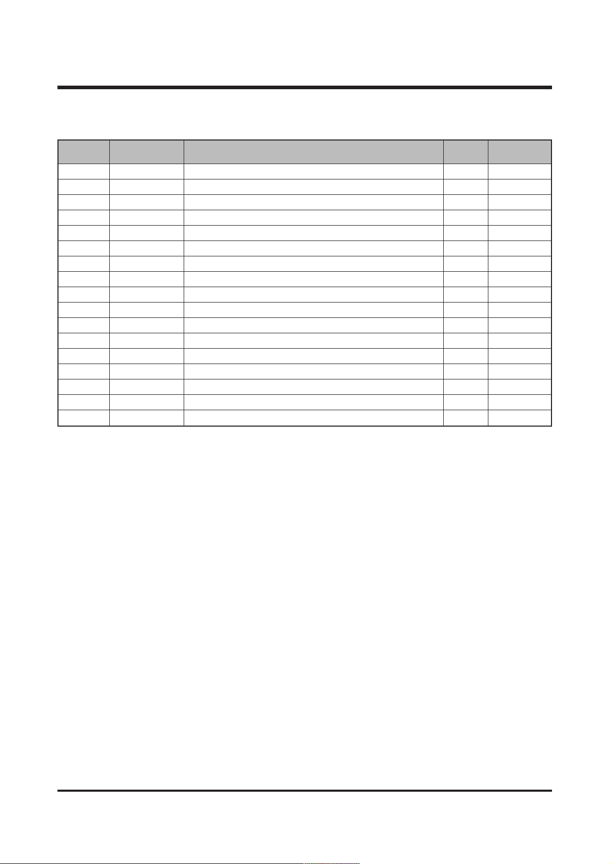
4. BACK COVER ASSEMBLY
4-1
4-3
4-2
4-4
4-14
4-8
4-11
4-6
4-5
4-10
4-7
4-12
4-9
4-13
Page 24
25
Ⅲ. EXPLODED VIEWS AND PARTS LIST
25
FFiigg..NNoo.. PPaarrttss NNoo.. PPaarrttss NNaammee QQ''ttyy RReemmaarrkkss
4-1 Q9007221001A BACK COVER ASS'Y 1
4-2 Q9007221001A BACK COVER SUB ASS'Y 1
4-3 Q7204020801A ZOOM BUTTON 1
4-4 Q7217340901A BACK COVER 1 white
Q7217341001A BACK COVER 1 silver
4-5 Q7204021101A LED GUIDE BACK 1
4-6 Q7217341101A DIRACTION BUTTON 1
4-7 Q7204021001A BUTTON 1
4-8 Q7204020901A OK BUTTON 1
4-9 Q7409175501A TFT SPONGE 1
4-10 Q7309044901A KEYPAD RUBBER 3
4-11 Q4719003601A METAL DOME 1
4-12 Q9008081201A KEY PCB ASS'Y 1
4-13 Q4102009901A FPC CABLE 1
4-14 Q6002024401A TAPPING SCREW 4
▶▶
PARTS LIST
Page 25
26
Ⅲ. EXPLODED VIEWS AND PARTS LIST
26
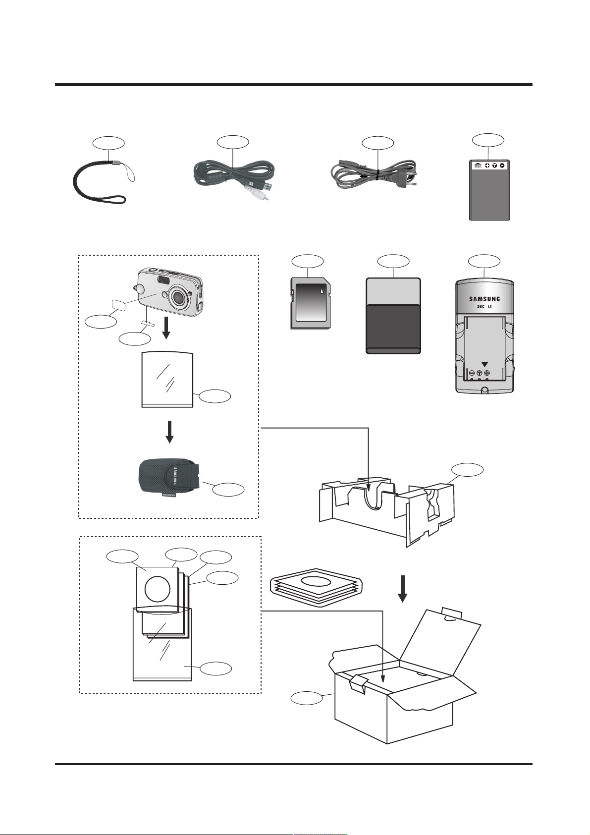
5. PACKING ITEM
5-9
5-12
5-18
5-1
5-10
5-16
5-14
5-15 5-135-17
CHARGE
5-11
5-5
5-3
5-4
5-6
5-7
5-2
5-5
Page 26
27
Ⅲ. EXPLODED VIEWS AND PARTS LIST
27
FFiigg..NNoo.. PPaarrttss NNoo.. PPaarrttss NNaammee QQ''ttyy RReemmaarrkkss
5-1 QP960210101A PE BAG (FOR CAMERA) 1
5-2 Q6909011601A PE BAG (FOR ACCESSORY) 1
5-3 Q6901202701A INNER PAD_U-CA 501/505 1
5-4 Q6904025901A POUCH_U-CA 501/505 1
5-5 Q6806234201A Q/GUIDE_U-CA 501/505_ENG 1
Q6806234301A Q/GUIDE_U-CA 501/505_GER 1
Q6806234401A Q/GUIDE_U-CA 501/505_FRA 1
Q6806234501A Q/GUIDE_U-CA 501/505_SPA 1
Q6806234601A Q/GUIDE_U-CA 501/505_ITA 1
Q6806234701A Q/GUIDE_U-CA 501/505_CHI(T) 1
Q6806234801A Q/GUIDE_U-CA 501/505_DUT 1
Q6806234901A Q/GUIDE_U-CA 501/505_POR 1
Q6806235001A Q/GUIDE_U-CA 501/505_SWE 1
Q6806235101A Q/GUIDE_U-CA 501/505_DEN 1
Q6806235201A Q/GUIDE_U-CA 501/505_FIN 1
Q6806235301A Q/GUIDE_U-CA 501/505_RUS 1
Q6806235401A Q/GUIDE_U-CA 501/505_CHI(S) 1
Q6806235501A Q/GUIDE_U-CA 501/505_TK 1
Q6806237101A Q/GUIDE_KENOX CD 5/ME 5 KOR 1
5-6 Q6806235601A U/MANUAL_U-CA 501/505_ENG 1
Q6806235701A U/MANUAL_U-CA 501/505_GER 1
Q6806235801A U/MANUAL_U-CA 501/505_FRA 1
Q6806235901A U/MANUAL_U-CA 501/505_SPA 1
Q6806236001A U/MANUAL_U-CA 501/505_ITA 1
Q6806236101A U/MANUAL_U-CA 501/505_CHI(T) 1
Q6806236201A U/MANUAL_U-CA 501/505_DUT 1
Q6806236301A U/MANUAL_U-CA 501/505_POR 1
Q6806236401A U/MANUAL_U-CA 501/505_SWE 1
Q6806236501A U/MANUAL_U-CA 501/505_DEN 1
Q6806236601A U/MANUAL_U-CA 501/505_FIN 1
Q6806236701A U/MANUAL_U-CA 501/505_RUS 1
Q6806236801A U/MANUAL_U-CA 501/505_CHI(S) 1
Q6806237001A U/MANUAL_U-CA 501/505_TK 1
Q6806237201A U/MANUAL_KENOX CD 5/ME 5 KOR 1
▶▶
PARTS LIST
Page 27
28
Ⅲ. EXPLODED VIEWS AND PARTS LIST
FFiigg..NNoo.. PPaarrttss NNoo.. PPaarrttss NNaammee QQ''ttyy RReemmaarrkkss
5-7 Q6807003003U WARRANTY CARD_EXP 1
Q6807010902B WARRANTY CARD_RUS(3 YEARS) 1
Q6807011301B WARRANTY CARD_TSOE(CHINA) 1
5-8 Q6901202801A G/T BOX_U-CA 501_EXP/AUS 1
Q6901202901A G/T BOX_U-CA 501_USA/CAN 1
Q6901203001A G/T BOX_U-CA 505_EXP/AUS 1
Q6901203101A G/T BOX_U-CA 505_USA/CAN 1
Q6901203301A G/T BOX_KENOX CD5 KOR 1
Q6901203401A G/T BOX_KENOX ME5_KOR 1
5-9 Q7409121701A STRAP_D301/D202/D401_KOR/EXP 1
5-10 Q3802003301A Y CABLE_U-CA 501/505 1
5-11 Q4609009601A
DRIVER+Digimax Viewer 2.1+Arcsoft PI 4.0+Digimax Reader
1
Q4609009701A
DRIVER+Digimax Viewer 2.1+Arcsoft PI 3.0(Walmart)+Digimax Reader
1
5-12 Q6804063301A PRODUCT STICKER_U-CA 501/505 1
Q6804063401A PRODUCT STICKER_U-CA 501_MEXICO 1
5-13 Q4301002601A DURACELL_LITHIUM BATTERY_CP1 1
5-14 Q4301003201A LITHIUM-ION_SLB-1137(SDI) 1
5-15 Q4309001601A SBC-L3 1
5-16 Q3801003201A AC CODE CABLE_EXP 1
Q3801003101A AC CODE CABLE_USA 1
Q3801001001A AC CODE CABLE_UK 1
Q3801003401A AC CODE CABLE_AUS 1
5-17 Q4602000701A SECURE DIGITAL CARD(64MB) 1
Q4602001301A SECURE DIGITAL CARD(128MB) 1
5-18 Q7409170701A FCC LABEL_U-CA 501/505_EXP (MADE IN CHINA) 1
Q7409170801A FCC LABEL_U-CA 501/505_EXP (MADE BY SAMSUNG) 1
Q7409170901A MIC LABEL_KENOX CD5/ME5_KOR (MADE IN CHINA) 1
▶▶
PARTS LIST
Page 28
ⅣⅣ.. AADDJJUUSSTTMMEENNTT
292929
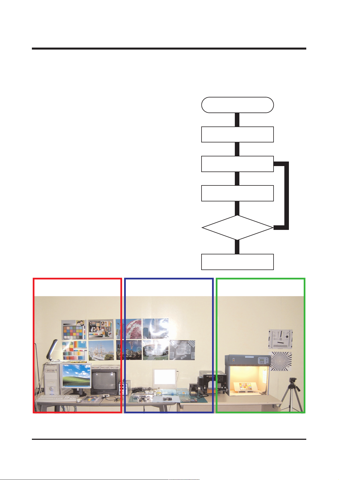
To take a digital camera service(Repair, Tuning and Checking), the following equipments have to be
arranged.
The sequences for the camera service are as shown
alongside.
1. Receiving the camera
When receiving a camera, check whether the accessories
are included or not and ask the customer exact problems.
2. Checking the camera
Checking the camera with priority given to the exact
problems to find overall malfunctions.
3. Repairing the camera
Repair the camera malfunctions found at the step 2.
4. Inspection
After repairing the camera, inspect all of the camera
functions.(See p.56)
292929292929
11.. CChheecckkiinngg tthhee ccaammeerraa aanndd
IInnssppeeccttiioonn
22.. RReeppaaiirriinngg tthhee ccaammeerraa 33.. TTuunniinngg
Receiving the camera
Checking the camera
Repairing the camera
Tuning
Inspection
Finish
11.. DDiiggiittaall ccaammeerraa sseerrvviiccee
※ The illustrations may be different from the real display in accordance with the camera model.
Page 29
30
Ⅳ. ADJUSTMENT
3030303030
11)) EEqquuiippmmeennttss ffoorr cchheecckkiinngg aanndd iinnssppeeccttiioonn
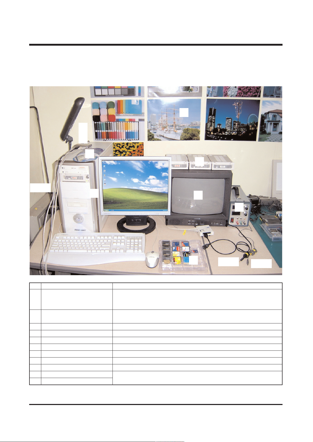
To check and inspect the camera malfunction, the following equipments have to be arranged.
①①
②②
③③
⑤⑤
⑥⑥
⑦⑦
⑧⑧
⑪⑪
⑨⑨
⑩⑩
④④
No. Device Description
1 PC for inspection - Installing a digital camera driver or Checking the removable device
- Checking the file transference(upload and download)
- Playing back the still image or movie clip
2 HARD RACK, For the compatibility test.
by Operating System by the O/S(WIN 98SE, ME, 2000, XP)
3 Driver CD, by camera models S/W CDs for installing a camera driver
4 USB HUB For using all kinds of USB cable at a time
5 USB cable, by camera models For checking file transference(upload and download) by camera models
6 Chart for checking colors For checking color and image resolution before or after camera repair
7 TV MONITOR For checking video output and whether NTSC/PAL can be selected
8 Memory card by types For checking card recognition by brands and sizes
9 A/V CABLE For checking whether the image can be displayed on a external monitor
10 POWER SUPPLY For checking camera power by camera models
11 Power cable by camera models
Page 30
31
Ⅳ. ADJUSTMENT
3131313131
①①
②②
③③
⑤⑤
⑥⑥
⑪⑪
⑨⑨
④④
⑩⑩
⑧⑧
⑪⑪
⑫⑫
⑬⑬
⑦⑦
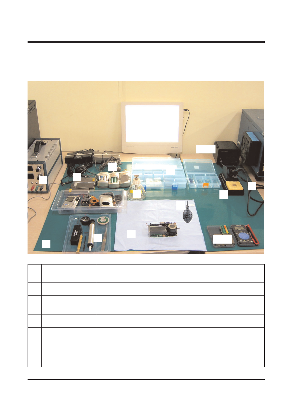
No. Device Description
1 A set of tools Pincette/ Screwdriver/ Discharger etc.
2 Cleaning paper For cleaning camera lens and camera parts
3 Detergent container For containing detergent
4 Parts case For keeping various camera parts and disassembled camera parts
5 Anti-electricity mat For repairing table made from anti-electricity material
6 Soldering sponge For removing solder
7 Air pump For removing various kinds of dust
8 LIGHT BOX Color temperature 5100
9 POWER SUPPLY 7.5V 2.0A
10 Soldering iron Soldering iron that can select temperature
11 Tester Portable tester that can test AC/DC, Ω,♪ ect.
12 BATTERY & AC ADAPTOR & Rechargeable battery by camera models
AC ADAPTOR - SBP3603/ SBP3605/ SBP3606
- SLB 1437
- SBP 1103
To repair the camera, the following equipments have to be arranged.
22)) EEqquuiippmmeennttss ffoorr ccaammeerraa rreeppaaiirr
Page 31
32
Ⅳ. ADJUSTMENT
3232323232
①①
②②
③③
⑤⑤
⑥⑥
④④
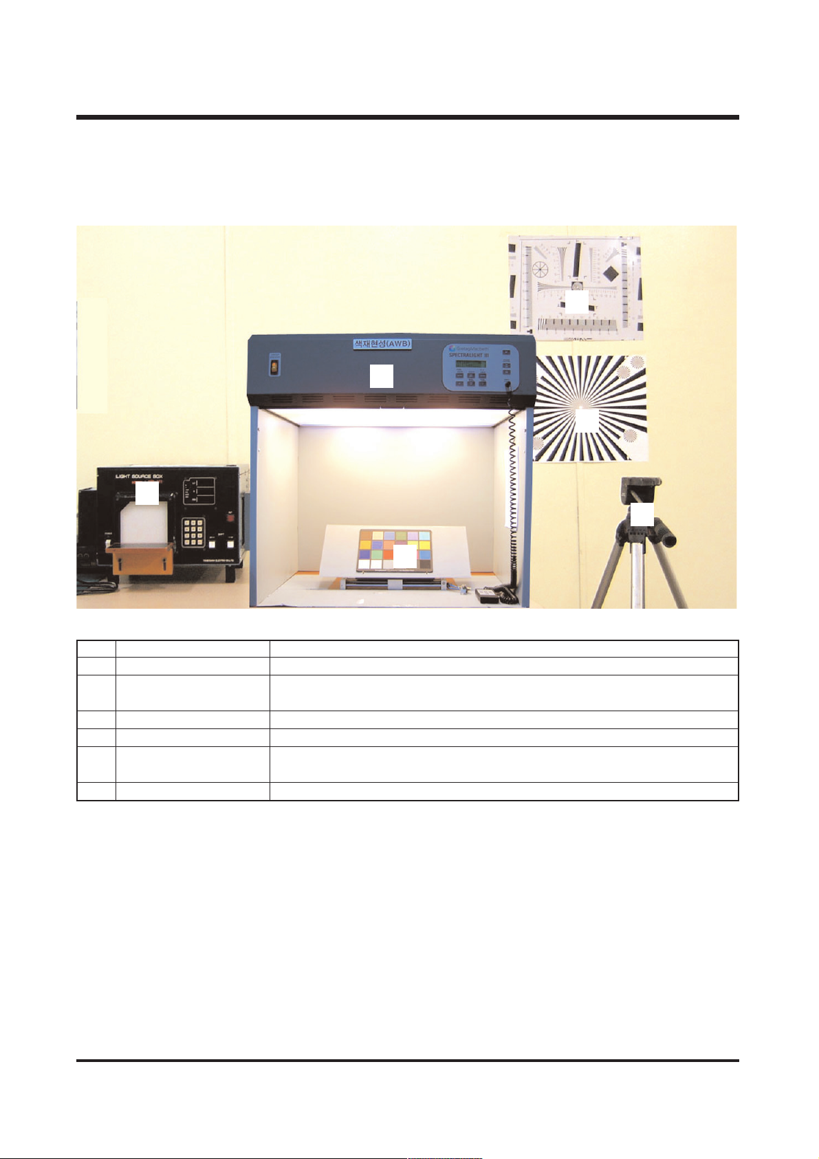
No. Device Description
1 AE TESTER For tuning AE and STROBE
2 AWB LIGHT For checking and tuning AWB
SOURCE BOX
3 COLOR chart For checking AWB and color of images
4 AF chart For tuning AF
5 Chart for checking For checking image resolution
resolution
6 TRIPOD
To tune the camera, the following equipments have to be arranged.
33)) EEqquuiippmmeennttss ffoorr ccaammeerraa ttuunniinngg
Page 32
33
Ⅳ. ADJUSTMENT
3333333333
44)) CChheecckk lliisstt ffoorr DDiiggiittaall ccaammeerraa rreeppaaiirr
To check the digital camera functions before/after repairing, refer to the check list.
NNoo.. CChheecckkiinngg iitteemm CChheecckk ppooiinntt
1 - Check the scratch, stain, misprint.
- Check whether the screws are turned firmly.
- Check the corrosion of terminal, bad exterior.
- Do chemical and glue test to the printing/ painting parts.
2 - Check the connecting and contact condition.
3 - Insert the batteries with the correct polarity and check the
contact condition.
- Check whether the cover is opened easily after closing.
4 - The card can be inserted or removed easily and cover is
closed firmly.
- Do inserting and removing card(SD/MMC) test two times.
→ The card must be inserted firmly and has not to spring out.
- Insert the card/batteries and give a little impact on the
camera. The camera must recognize the card and “CARD
LOCKED”message has not to be displayed.
5 - When the cable is inserted, check whether the images play
back on the external monitor.
6 - Check whether the green LED is blinking, SAMSUNG LOGO is
on and the start-up sound sounds.
- Check the “L”and “FINE”icon on the LCD monitor.
- Check whether the AE function is correct at the low light and
high light condition.
- Check whether the “beep”sounds on the recording and movie
clip mode.
→ The “beep”can be sounded in the microphone part. Check
that in a quiet room.
7 - Press the zoom W/T button with the viewfinder.
→ Check dust and percentage of the frame seen, zoom rate.
- Press the zoom W/T button with the TFT-LCD monitor.
→ Check the zoom rate and whether the zoom bar moves
smoothly.
8 - Check whether the Macro icon(Flower) is displayed on the
LCD monitor.
- Check the AF in the Macro focus with the TFT-LCD monitor.
9 - Check whether the subject captured from 2M has over or
under exposure and the fucus is clear.
Check the exterior of a camera.
Insert the adapter.
Check the battery cover.
Check the card condition after
inserting the card.
Insert the Video cable.
Turn on the camera.
Press the zoom W/T button.
Macro focus.
Normal focus.
Page 33
34
Ⅳ. ADJUSTMENT
3434343434
NNoo.. CChheecckk iitteemm CChheecckk ppooiinntt
10 - Check whether the icon and counter are displayed on the
LCD monitor.
11 - Check whether the recording time is displayed and there
are a noise, dim frame and discontinuous frame in the movie
clip.
12 - Check whether the zoom rate is changed and there are
unclear part, noise and dim part in the image.
- The distance from the subject is 2M and have to use the
FILL IN flash.
13 - Check whether the PLAY mode can be selected without any
problem and there are any noise, frame shaking and
discoutinuous frame.
- Check the voice recorded in the still image and the movie clip.
- Check whether the still image can be enlarged correctly
with the 5 function button.
14 - Select 2 sec. of slide show interval time and check whether
there are any noise, image shaking and discontinuous frame.
15 - Check whether the mode dial is rotated with the equal force.
- Check whether each camera mode can be recognized correctly.
16 - Check whether there are unclear part, dim part, noticeable
flare, noise, ghost image and smear.
17 - Check whether all images are deleted.
18 - Check whether the “NO IMAGE”message is displayed on the
LCD monitor.
- Check whether the LARGE, FINE icon and 0018 number are
displayed.
- Check whether the camera power is turned off without any
problem.
MANUAL focus.
Take a movie clip with
TELE zoom during 10 seconds.
Take a chart with TELE zoom
in a low light condition.
Play back a image with
the TFT LCD monitor.
Start the slide show
in the PLAY mode.
Try to rotate the mode dial.
Download a image from a PC
with USB cable and check the
image quality in a external
monitor.
Format the card in the PLAY
mode.(Delete all images in the
PLAY mode)
Check whether there is no image
and reset the camera. Remove
the card and turn off the camera.
Page 34
35
Ⅳ. ADJUSTMENT
3535
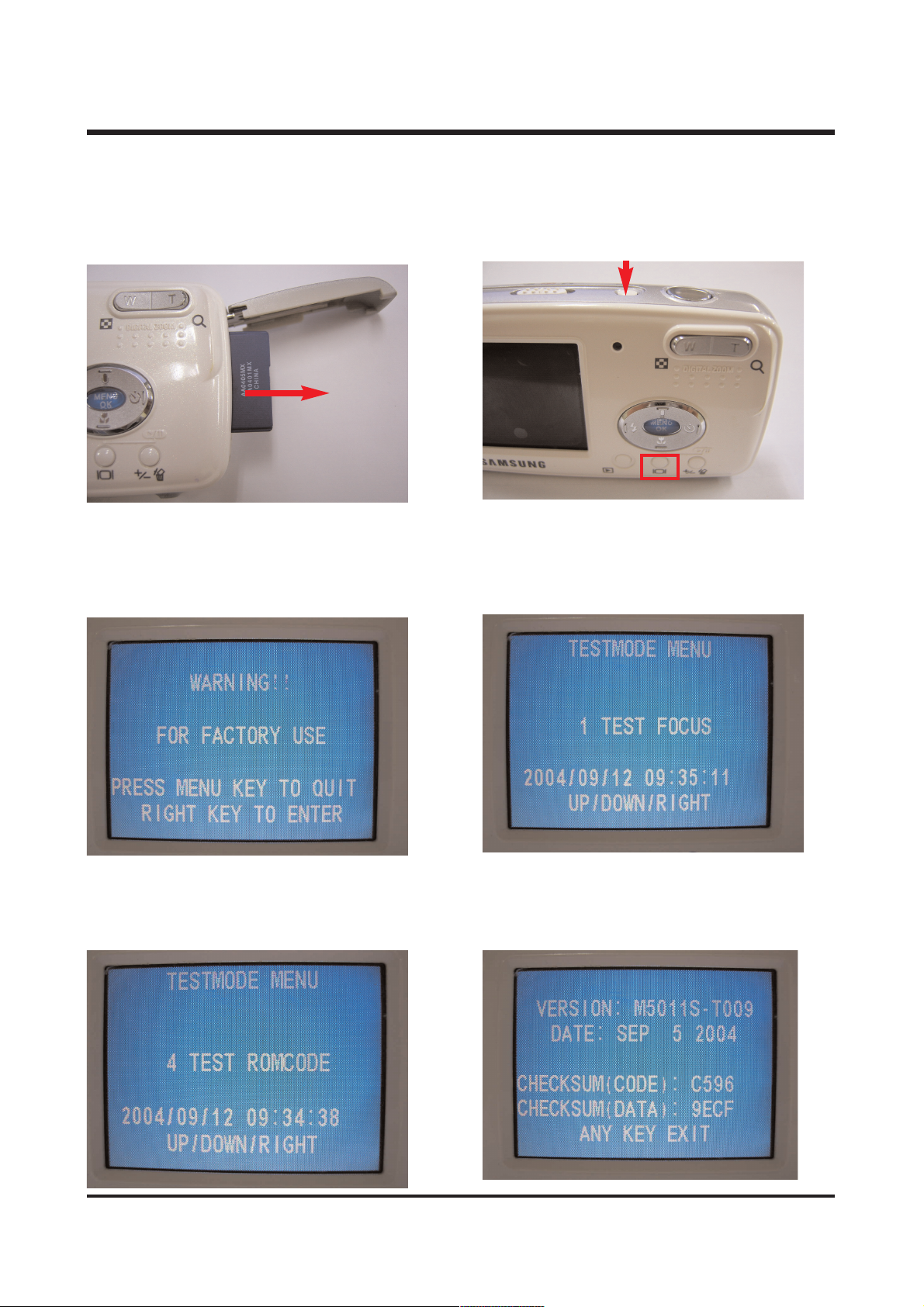
5. Press the right key to check the firmware. 6. Check the Firmware version.
3. When you enter the test mode, press right
Romcode.
4. Press the down key to enter the TEST
key to enter the next mode.
1. Remove the SD card from camera. 2. Press the Power on button while pressing the
LCD button.
35353535
22.. HHooww ttoo cchheecckk tthhee FFIIRRMMWWAARREE VVEERRSSIIOONN
Page 35
36
Ⅳ. ADJUSTMENT
363636363636
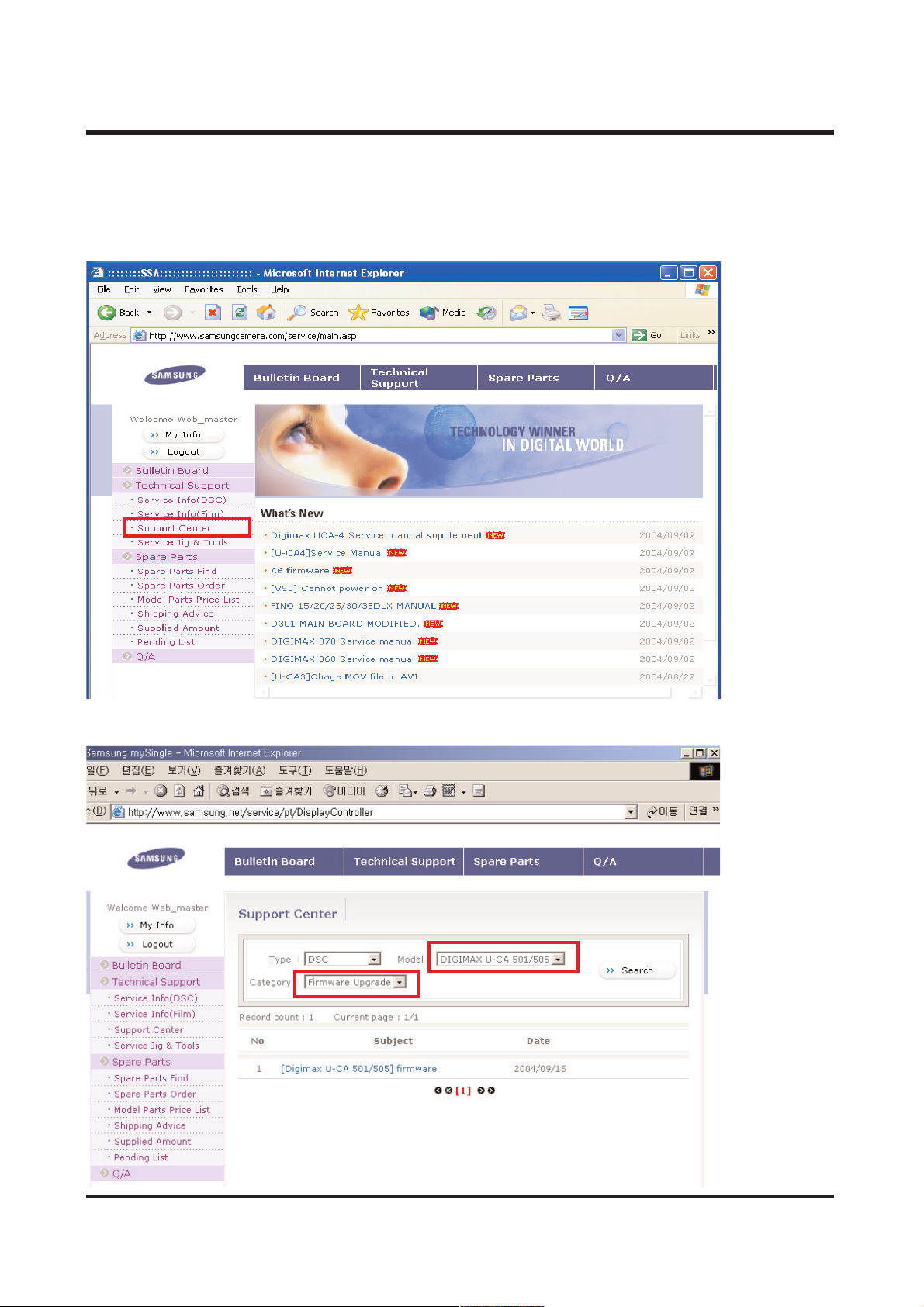
33.. HHooww ttoo uuppddaattee tthhee FFIIRRMMWWAARREE UUPPGGRRAADDEE
1. Connect the service site ‘www.samsungcamera.com/service’and click the Support center menu on
the left side menu.
2. Select the model and category.
Page 36
37
Ⅳ. ADJUSTMENT
3737
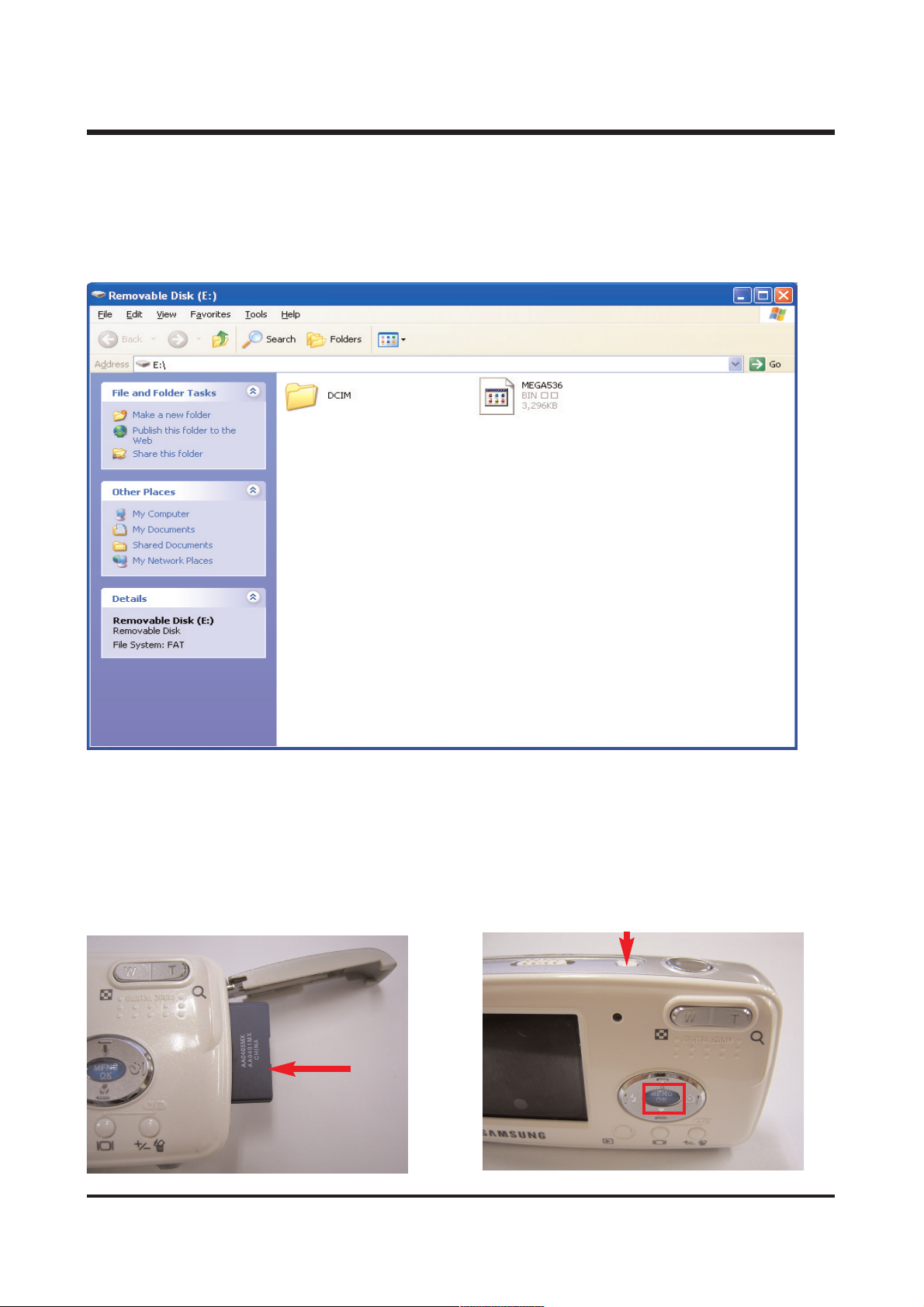
.4. Insert the SD card that has the firmware. 5. Turn on the power while preesing the LCD
button.
37373737
3. Download the MEGA536 to the windows directory and copy to the removable disk after connecting
the camera. (Do not use card Reader)
Caution ) Format the SD card using the camera
After copying the file, check the file name.
Page 37
38
Ⅳ. ADJUSTMENT
383838383838
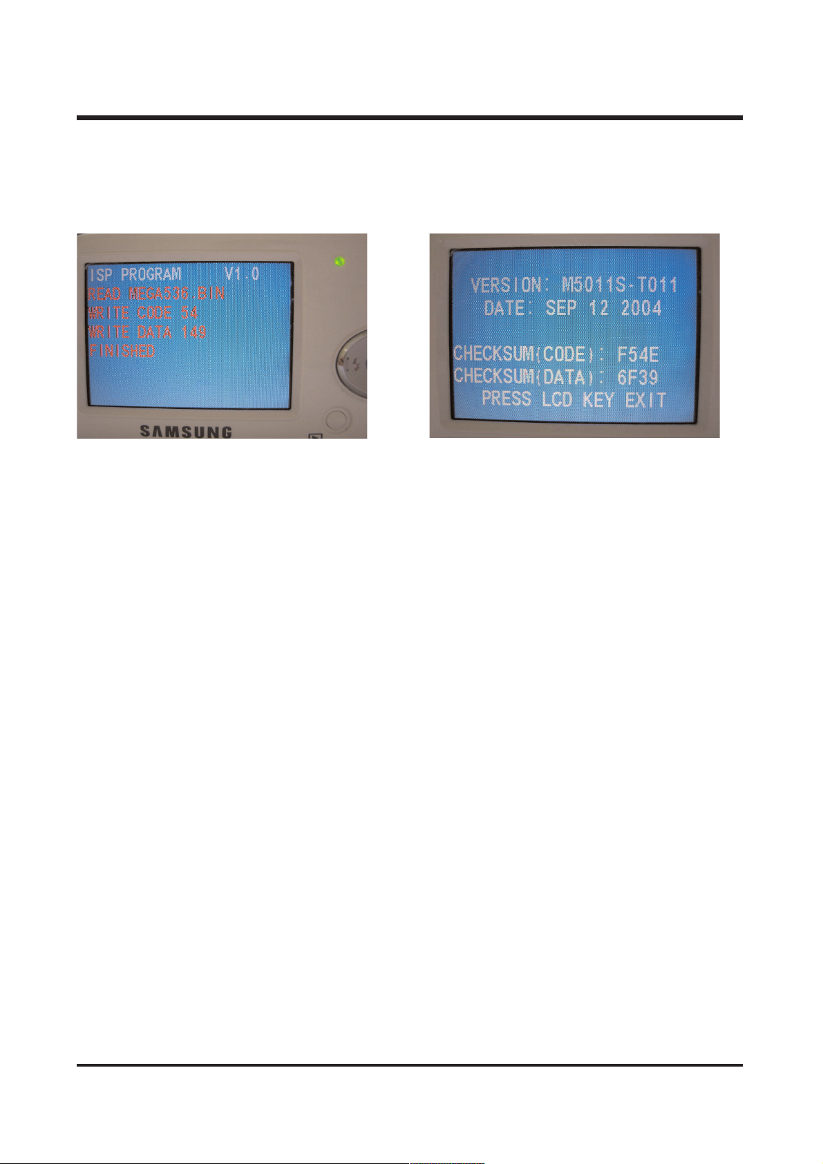
5. The green LED is blinking while the update is
progress. When the update is completed,
FINISH message is shown on the LCD.
6. Check the firmware that is updated.
※※ WWhheenn yyoouu ddoo tthhee FFiirrmmwwaarree uuppggrraaddee,, yyoouu hhaavvee ttoo uussee ffuullll cchhaarrggeedd bbaatttteerryy..
IIff tthhee ccaammeerraa ttuurrnnss ooffff wwhhiillee uuppddaattiinngg,, tthhee ccaammeerraa ccoouullddnnoott wwoorrkk..
AAfftteerr uuppddaattiinngg ffiirrmmwwaarree,, yyoouu hhaavvee ttoo rreesseett tthhee ccaammeerraa..
Page 38
39
Ⅳ. ADJUSTMENT
After changing the electronic parts of Digimax A5/A6the parts have to be tuned in accordnce with the
tuned items. The items listed on the table have to be tuned after change.
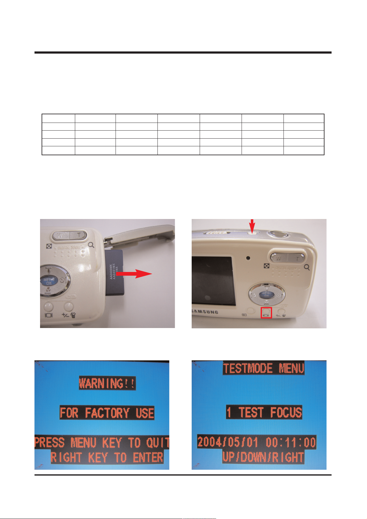
11)) TTEESSTT MMOODDEE
a. Remove a card from camera. b. Press the POWER ON button while pressing
OK button
C. When pressing the power button for 2 sec, d. Press the RIGHT BUTTON then, the TEST MODE
beep sound comes out with below screen. is executed.
39
Main Board Flash Board Key board CCD TFT LCD Lens Unit
Focus ● ● ●
MSCALIB ● ●
BATTERY ●
BAD PIXEL ● ●
44.. AADDJJUUSSTTMMEENNTT
Page 39
40
Ⅳ. ADJUSTMENT
40
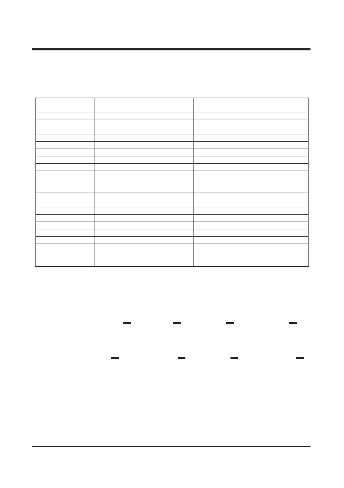
The below section can be executed by entering the TEST MODE.
1) TEST FOCUS : Refer to the adjustment.
2) TEST MSCALIB : Refer to the adjstment.
3) TEST BURNIN
Check the each function and capability of camera.
▶ Check the working condition for 30 Mins.
Charge and strobe of camera Check SDRAM Check EEPROM Check MSSHUTTER
ZOOM, AF
After 30Mins, detect the HOT and BAD PIXEL(WHITE).
▶ Last 30Mins check below items.
Change the IMAGE SIZE Change the QUALITY FLASH ON/OFF Record Movie(Time)
After taking picture, (DELETE ONE, DEL ALL, FORMAT) is executed.
4) TEST ROMCODE
Check the Firmware version.
a. Select the No.4 of TEST MODE and press Right Key. The firmware version will be shown (Refer to
the firmware version.)
404040
NO. TEST ITEM EQUIPMENT REMARKS
1 TEST FOCUS AF CHART ADJUSTMENT
2 TEST MSCALIB LV 15 ADJUSTMENT
3. TEST BURNIN POWER SUPPLY
4. TEST ROMCODE
5. TEST STROBE
6 TEST EEPROM
7 TEST LENS
8 TEST BUZZER
9 LIFE TEST
10 TEST CARD SD CARD
11 TEST NAND
12 TEST SDRAM
13 TEST BATTERY POWER SUPPLY ADJUSTMENT
14 TEST COLORBAR
15 TEST KBD
16 CCD COLOR Not use.
17 BAD PIXEL LV12 ADJUSTMENT
18 CCD TIME Not use.
19 RESET Not use.
20 QA LIFE TEST Not use.
21 SHOW EEPROM VALUE Not use.
22 DEFOCUS
22)) TTEESSTT SSEECCTTIIOONN
Page 40

41
Ⅳ. ADJUSTMENT
41
5) TEST STROBE
Check the charging and radiation of FLASH with below order.
- REDY PIN CHECK : When the charging is completed, “STROBO IS READY”will be shown,
if the charging is not completed, “STROBO NOT READY" will be shown.
- CHARGE STROBE : Press the RIGHT KEY to execute the charging.
- TRIGGER : Press the RIGHT KEY to execute the radiation.
- TRIGGER ONCE : Press the RIGHT KEY to execute the radiation once more.
- TRIGGER LOOP : Press the RIGHT KEY to loop the radiation.
6) TEST EEPROM
Check the condition of EEPROM
Press the RIGHT KEY to read the data for adjustment in EEROM and check the working condition of
EEPROM.
7) TEST LENS
Check the working condition of LENS UNIT, Apperture and shutter.
- APERTURE : Aperture OPEN/CLOSE
- MSHUTTER OPEN : Shutter OPEN/CLOSE
- AP+MS O/C : Aperutre and shutter opens and closes continually at the same time.
- ZOOM CAL : Press the OK to execute ZOOM.
- AF CAL : Check the AUTO FOCUS
- AF CLOSE : Press the OK to execute out focusing.
- ZOOM CLOSE : Press the OK to execute ZOOM OFF.
- MSHUTTER O/C : Shutter opens and closes continually.
- APERTURE O/C : Apertuer opens and closes continually.
8) TEST BUZZER
Check the Buzzer working condition and the type of buzzer, ON, ERROR, OFF.
9) LIFE TEST
Check the working condition. It only tests the picture-taking section for one time or continually.
IMAGE SIZE, IMAGE QUALITY, STROBO ON/OFF can be set for test.
10) TEST CARD
Check the regognization of SD card. Insert SD card and select this section then the “CARD INSERTED”,
will be shown. the “NO CARD”will be shown without card.
11) TEST NAND : Show the storage contents of internal memory and ERASE ALL function.
12) TEST SDRAM : Check the SDRAM
13) TEST BATTERY : Refer to the adjustment.
14) TEST COLORBAR
Check the color condition of TFT LCD. Check the color of 9 section.
1. Vertical COLOR BAR 2. Black and white BAR 3. RED 4. GREEN 5. BLUE
6. BLACK 7. WHITE 8. Horizontal COLOR BAR 9. Check the presentataion of COLOR
15) TEST KEBD
Check the working condition of each KEY and button.
Page 41
42
Ⅳ. ADJUSTMENT
424242
33)) AADDJJUUSSTTMMEENNTT IITTEEMMSS
11)) FFOOCCUUSS
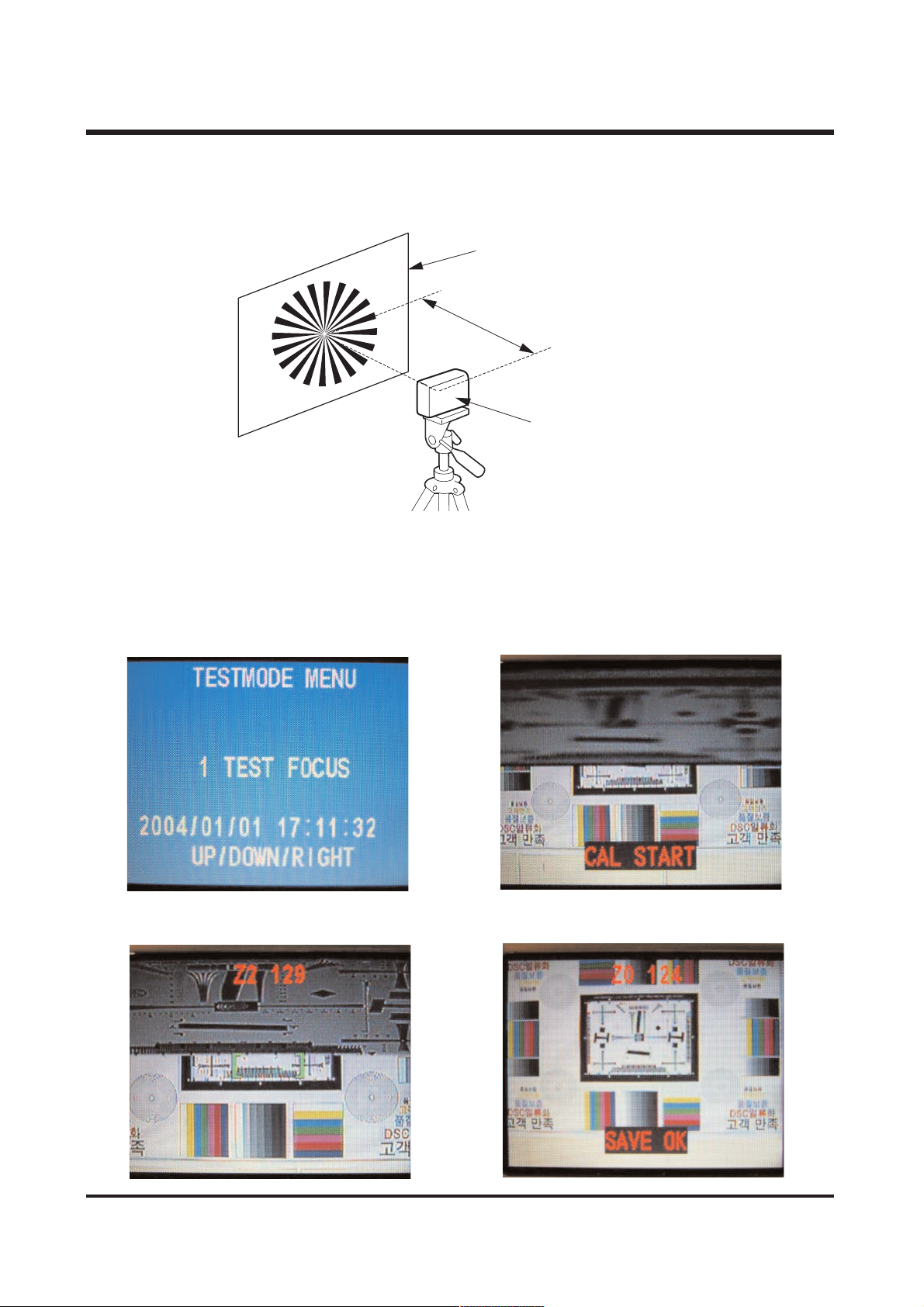
<How to adjut>
a. Set the SF CHART.
b. Put the camera on tri-pod.
c. Put the camera 2m away from the chart.
d. Select the TEST FOCUS in TEST MODE e. The adjustment will be automatically done
and press the RIGHT BUTTON. by pressing SHUTTER BUTTON.
f. Adjust the each step. g. The adjustment is completed.
2m
AF Chart
Tripod
Camera
Page 42
43
Ⅳ. ADJUSTMENT
43
22)) MMSSCCAALLBB
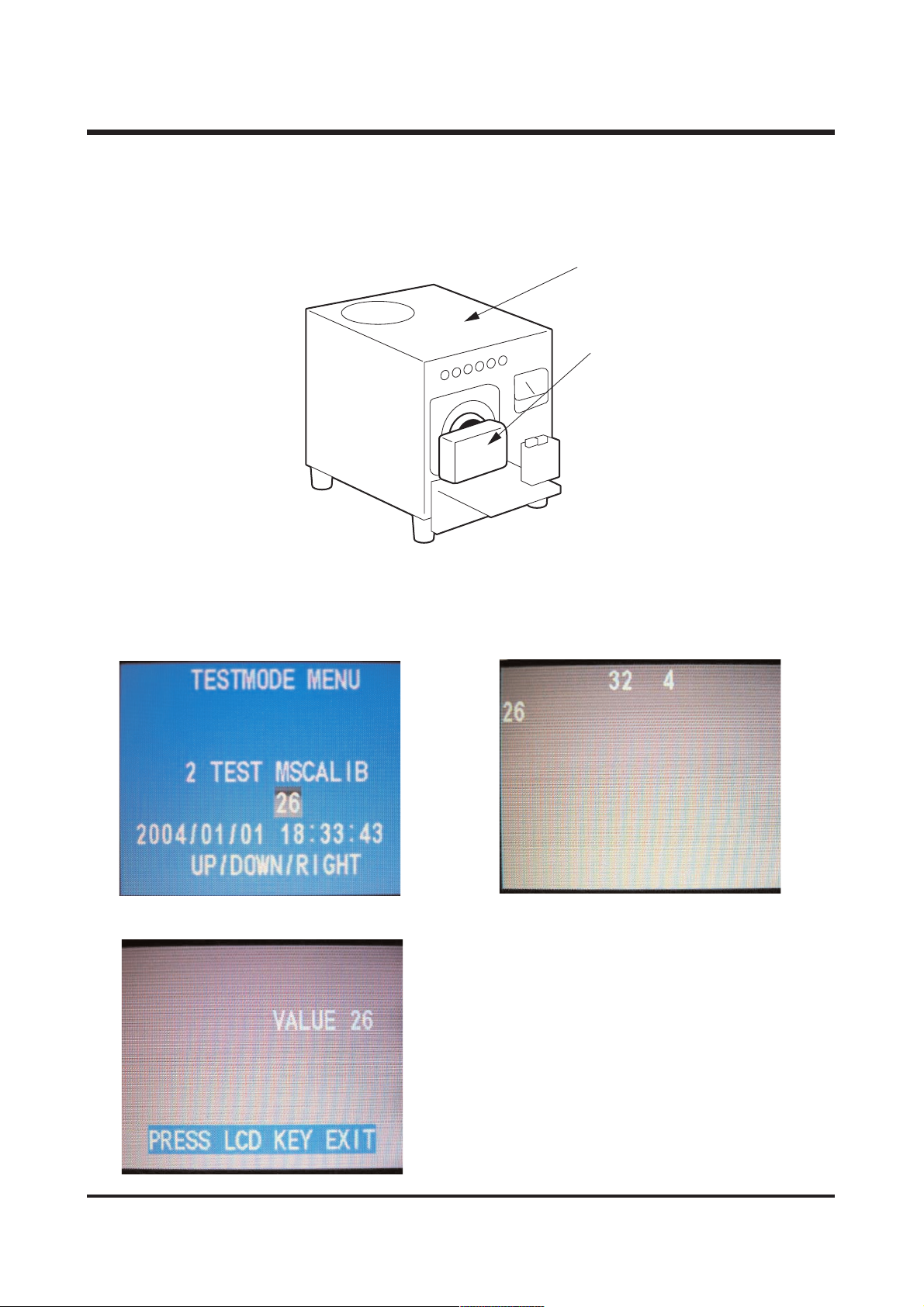
Equipment> AE TESTER (LV15)
<How to adjus>
a. Enter the TEST MODE.
b. Set the LIGHT SOURCE BOX to LV 15
c. Choose the TEST MSCALB. d. Press the RIGHT BUTTON to execute.
e. The adjustment is completed.
Light source box
Camera
Page 43
44
Ⅳ. ADJUSTMENT
44
33)) BBAATTTTEERRYY
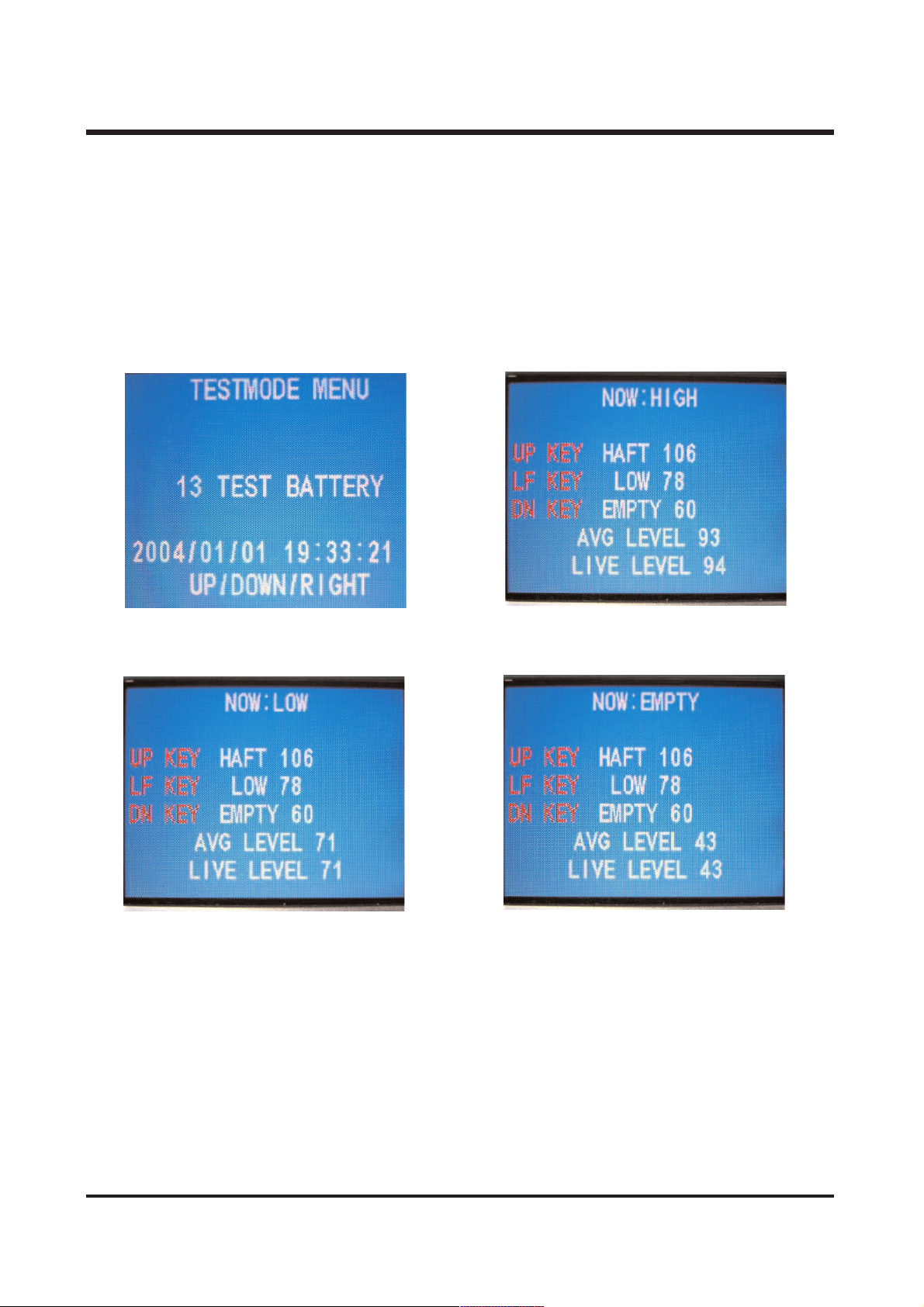
Equipment> POWER SUPPLY (2.2V, 2.0V, 1.8V)
<How to adjust>
a. Enter the TEST MODE.
b. Connect the POWER SUPPLY with camera.
c. Select the TEST BATTERY. d. Set the POWER SUPPLY to 2.2V and press
Then, press the RIGHT BUTTON. the UP BUTTON to adjust HIGH.
e. Set the POWER SUPPLY to 2.OV and press f. Set the POWER SUPPLY to 1.8V and press
the LEFT BUTTON to adjust LOW. the DOWN BUTTON to adjust EMPTY.
Page 44
45
Ⅳ. ADJUSTMENT
45
44)) BBAADD PPIIXXEELL
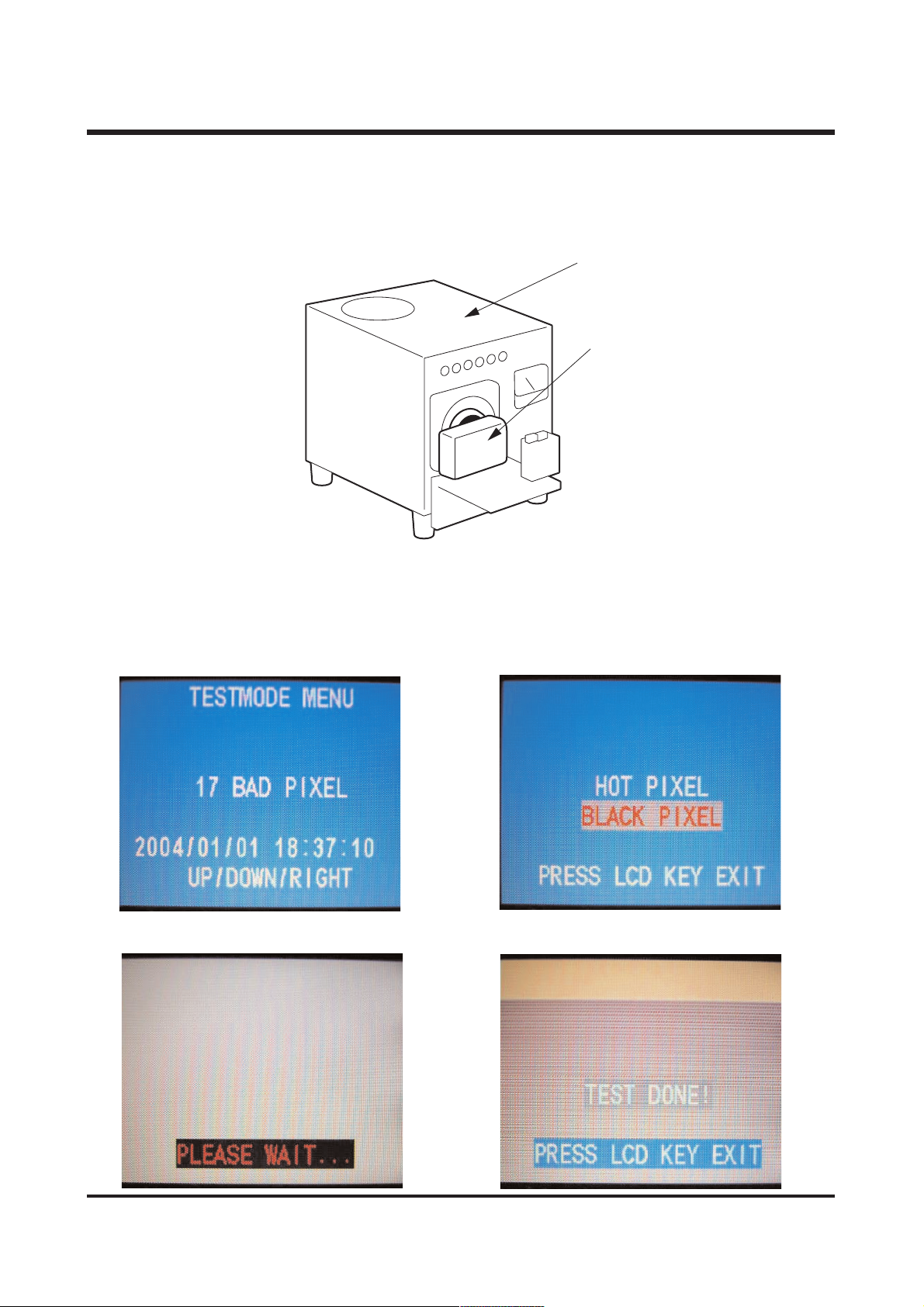
Equipment> AE TESTER (LV12)
<How to adjust>
a. Enter the TEST MODE.
b. Set the LIGHT SOURCE BOX to LV 12 and K=1.3.
c. Select the BAD PIXEL. d. The HOT and BLACK will be shown when
pressing the RIGHT BUTTON. Select the BLACK.
e. The adjustment is executed. f. The adjustment is completed.
Light source box
Camera
Page 45
46
Ⅳ. ADJUSTMENT
46
55)) DDEEFFOOCCUUSS
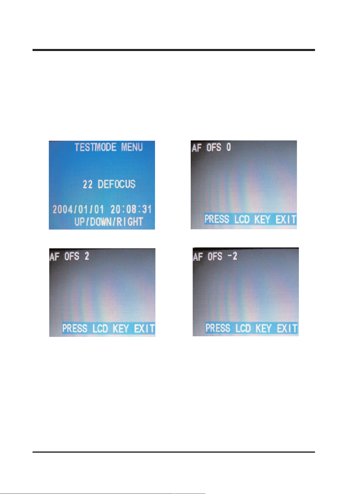
If the focus is not exactly fit evenif the focus adjustment is done, do the defocus to fit the focus by
moving the lens unit back and forth.
<How to adjus>
a. Enter the TEST MODE
b. Select the DEFOCUS. c. Press the RIGHT BUTTON to show the
initial value. (The initial value is “0”)
d. AF POSITION can be adjusted from +2 ~ -2.
Page 46
ⅤⅤ.. PPAATTTTEERRNN DDIIAAGGRRAAMM
47474747
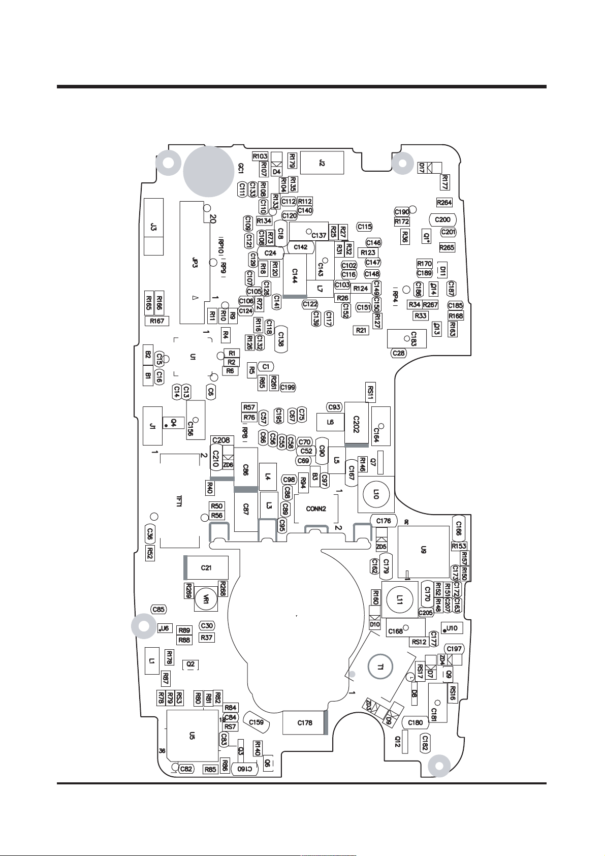
1. PARTS ARRANGENENT FOR EACH PCB ASS'Y
1) MAIN_TOP
Page 47
48
Ⅴ. PATTERN DIAGRAM
484848
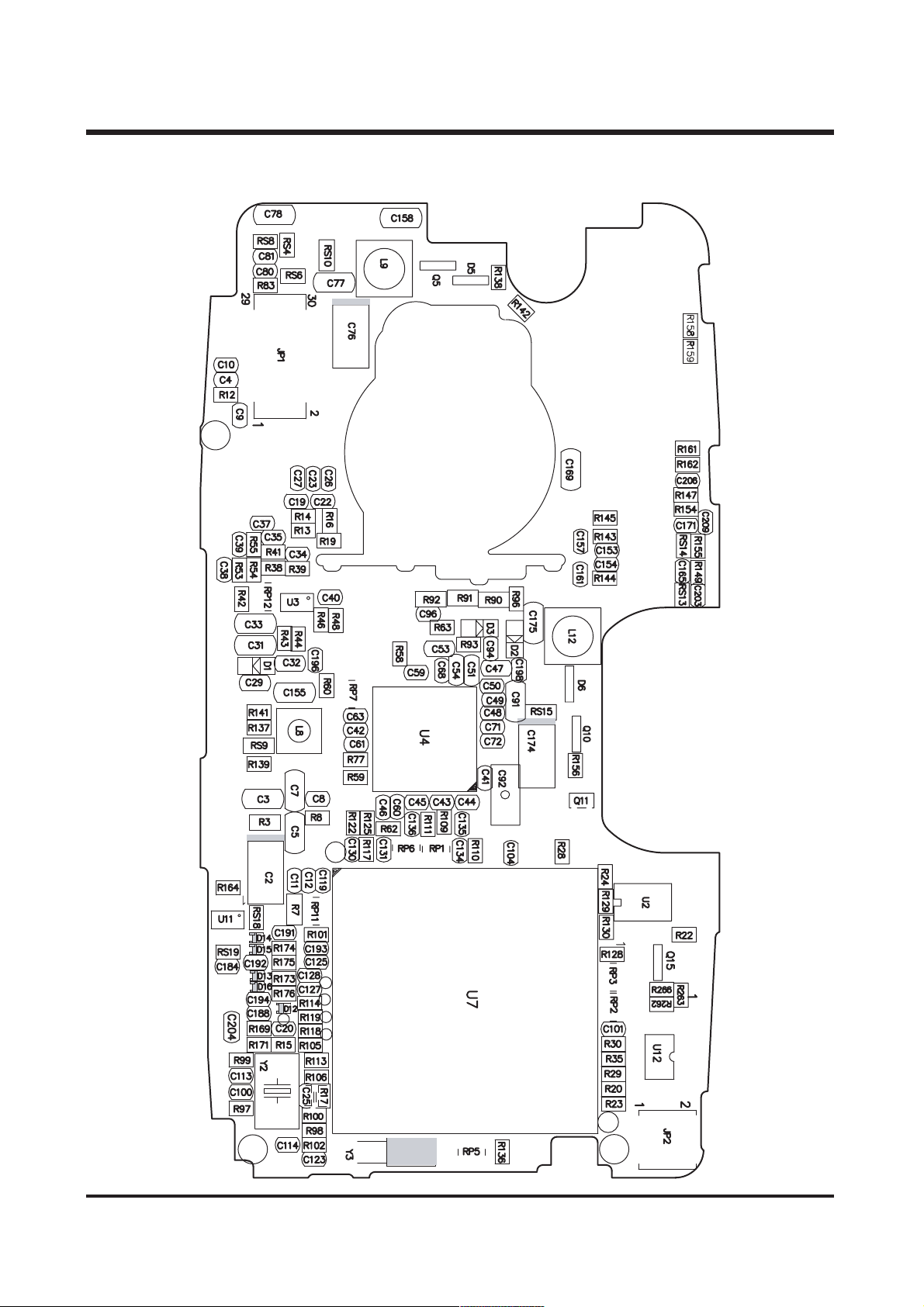
2) MAIN_BOTTOM
Page 48
49
Ⅴ. PATTERN DIAGRAM
494949
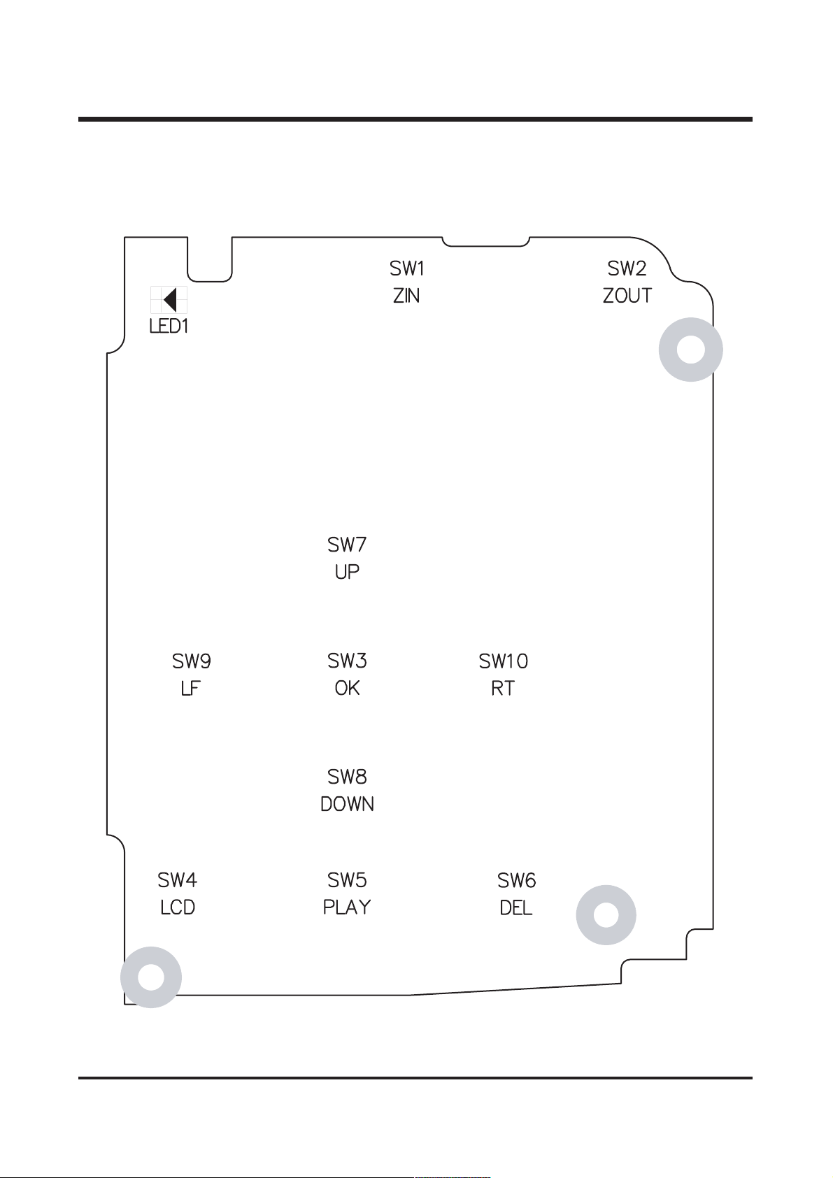
3) KEY_TOP
Page 49
50
Ⅴ. PATTERN DIAGRAM
505050
4) KEY_BOTTOM
Page 50
51
Ⅴ. PATTERN DIAGRAM
515151
5) FLASH_TOP
Page 51
52
Ⅴ. PATTERN DIAGRAM
525252
6) FLASH_BOTTOM
Page 52
53
Ⅴ. PATTERN DIAGRAM
535353
7) CCD_TOP
Page 53
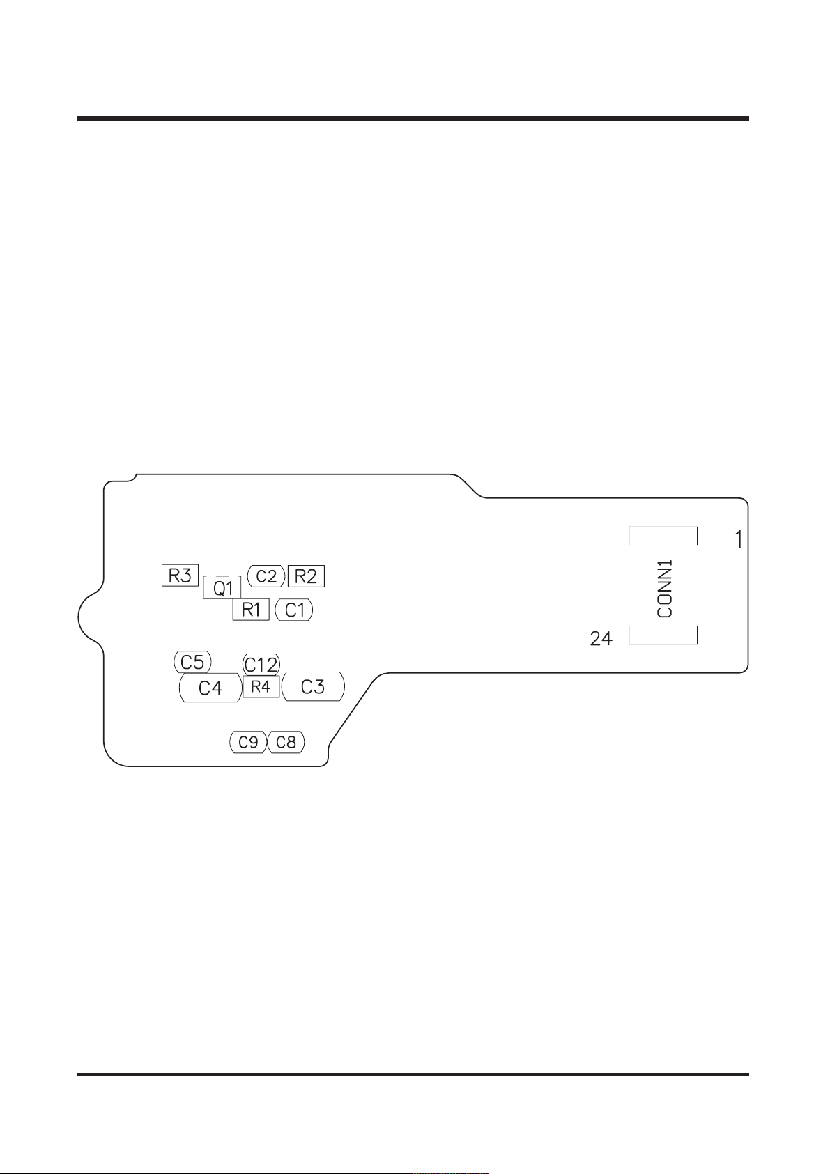
54
Ⅴ. PATTERN DIAGRAM
545454
8) CCD_BOTTOM
Page 54
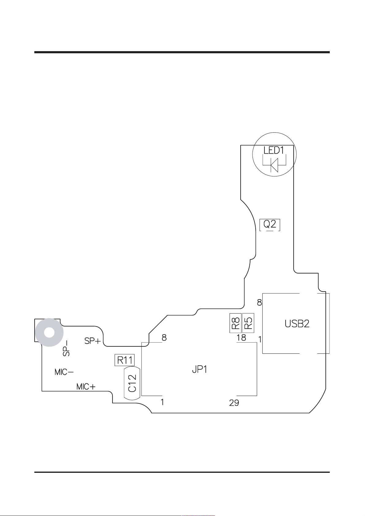
55
Ⅴ. PATTERN DIAGRAM
555555
9) USB_TOP
Page 55
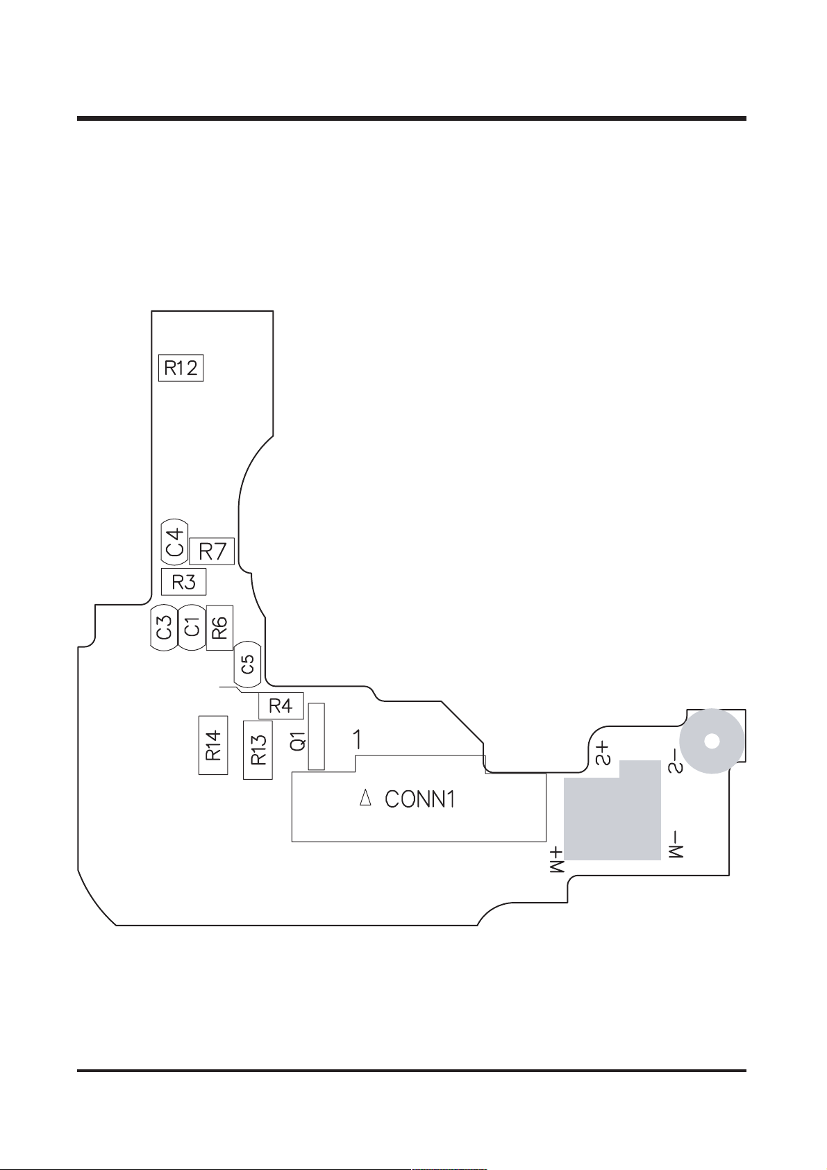
56
Ⅴ. PATTERN DIAGRAM
565656
10) USB_BOTTOM
Page 56
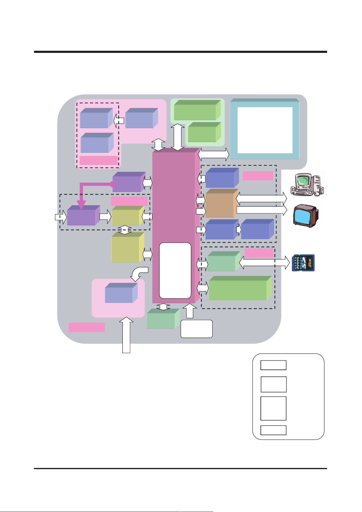
ⅥⅥ.. CCIIRRCCUUIITT DDIIAAGGRRAAMM
57
11.. BBLLOOCCKK DDIIAAGGRRAAMM
57575757
STRBOE
FLASH
Mode SW
Shutter Key
Power Key
ShutterBoard
[Charge IC]
Aimtron
AT1453
Strobe Charge Circuit
Status
indicator
Auxi-Focus
Light
[TFT-LCD]
Casio
COM20T2123
(2.0")
Image
[AFLens]
Samsung
SAA5025
MainBoard
[Motor IC]
ROHM
BD6758KN
SensorBoard
[CCD Sensor]
Panasonic
MN39482
[AFE/VD/T
G]
Panadonic
AN12062A
[Power IC]
Maxim
MAX1566
Power Supply Circuit
[DSP]
Sunplus
SPCA535 MCM
SDRAM 16Mx16
NAND Flash
[EEPROM]
Atmel
93C66
16M
[Crystal]
Main-27MHz
RTC-32.768KHz
Microphone
USB1.1
&
TV Out
[DAC]
Wolfson
WM8751
Card
Connector
OK/Menu/Del
Function Key
USB Board
Speaker
KeyBoard
Secure Digital Card
&
Multi Media Card
Battery - In
NP-60
CP-1
SYSTEM
CCD
TFT-LCD
AF_Lens
->P1V8_SYS
->P3V3_SYS
->P12V_CCD
->P3V3_CCD
->N8V_CCD
->P15V_TFT
TFT_BL +
->TFT_BL -
->P5V_SYS
->P3V3_SYS
->P4V_MOTO
->P3V3_SYS
Page 57
58
Ⅵ. CIRCUIT DIAGRAM
58585858
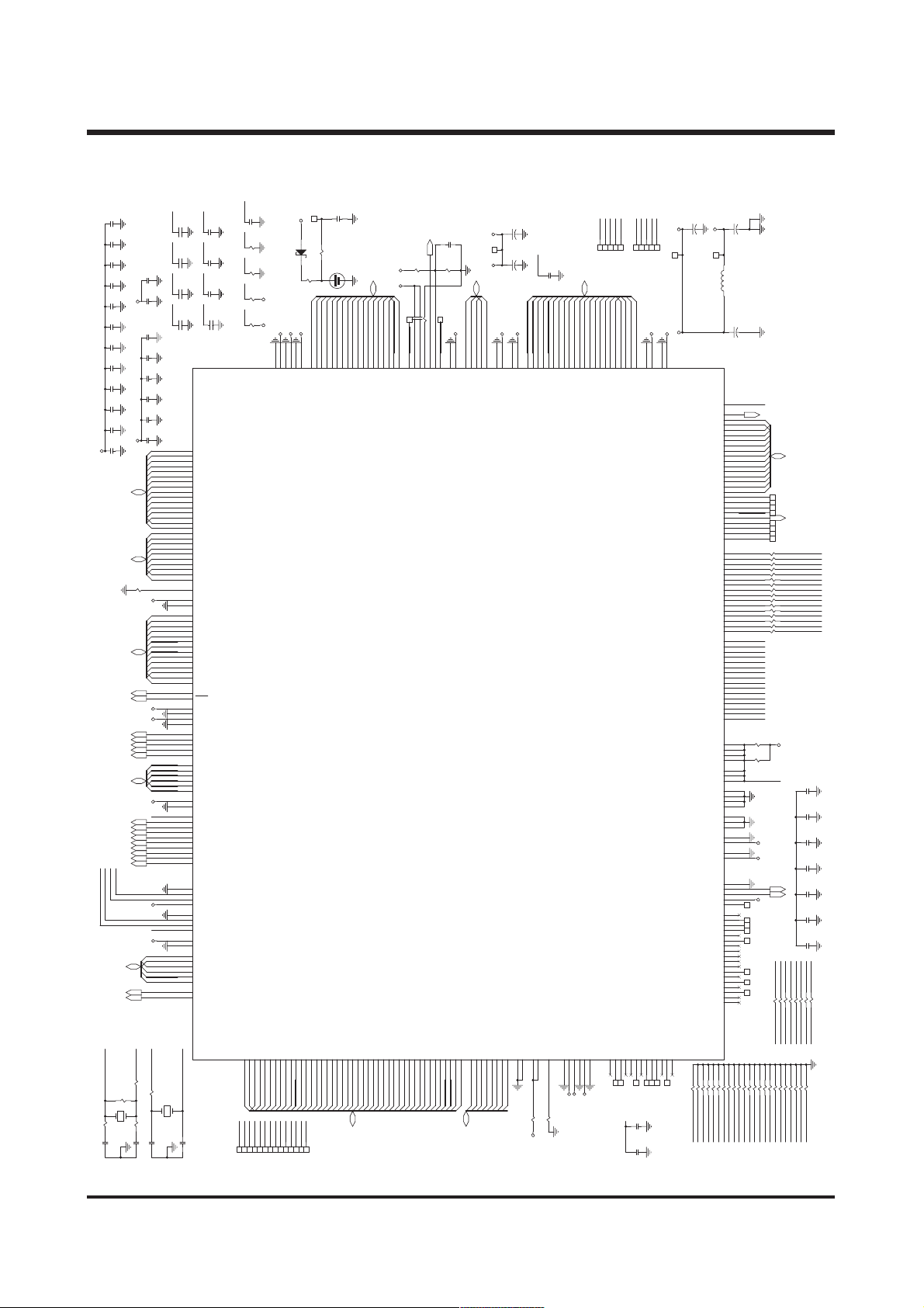
22.. CCIIRRCCUUIITT DDIIAAGGRRAAMM
1) TOP VIEW
TGGPIO26
TGGPIO27
TGGPIO28
TGGPIO29
TGGPIO38
TGGPIO39
TGGPIO43
TGGPIO41
DIGTV18
DIGTV19
DIGTV20
DIGTV21
IRIS_01
IRIS_02
IRIS_03
IRIS_04
TGGPIO38
TGGPIO20RESETb
TGGPIO39
MICP
MICP
OPI
MICN
MICN
OPO
AGC
AGC
A_VREF
SHUT
TRAP
TRAP
AGCOUT
STBVD
HD STO
TGGPIO30
TGGPIO31
MA[14..0]
MA[14..0]
DIGTV[21..0]
COUT
NOE
CDS_SDI
CDS_D[9..0]
CDS_SEN
TGGPIO37
RGB[9..0]
RESETb
RESETb
AUDP[5..0]
CDS_SCK
CDS_ADCCLK
CCD_SUBCTRL
TGGPIO40
FMGPIO[42..0]
FMGPIO[42..0]
CHB
CHC
JTAG_TRSTJTAG_CLK
CDS_CLCCD
N
MOTO_E
GPIO7
DM
DP
DP
DM
JTAG_TMSJTAG_TDI
IRIS_IN2
IRIS_IN1
AF_IN1
AF_IN2
GPIO0
GPIO1
JTAG_TDO
DRAMGPIO[3..5]
IRIS_IN3
IRIS_IN4
AF_IN3
AF_IN4
GPIO2
GPIO3
GPIO[15..0]
AF_HOME
TGGPIO12
TxD0
RxD0
TXD0
RXD0
TGGPIO[47..0]
RGB[9..0]
IRIS_02
IRIS_03
IRIS_01
AF_01A
AF_02A
AF_01B
AF_01A
AF_02A
AF_01B
AF_02B
01 SPCA536 DSP
IRIS_04
AF_02B
AF-E
AF-C
02 Image Peripheric circuit
AF-C
AF-E
DIGTV1
DIGTV2
TFT_D0
TFT_D1
TFT_D2
T
L
TFT_GRES
TFT_PO
TFT_GSR
DIGTV3
DIGTV4
TFT_D3
TFT_D4
H
B
TFT_ST
TFT_ST
EE_CS
EE_SCK
RESETb
TRAP
TRAP
DIGTV5
DIGTV6
TFT_D5
TFT_RIT
TFT_STBY
TFT_CLK
TFT_GPCK
TFT_CP
EE_SDI
MA[14..0]
MA[14..0]
04 TFT LCD
ISP
ISP
SP+
SP-
SP+
MIC+
MIC- SP-
03 TRAP / EEPROM
OPI
AU_CK AU_DA
OPI
MICN
OPO
A_VREF
OPO
MICP
TGGPIO39TGGPIO38
AGC
A_VREF
AUDP[5..0]
MCLK
AGC
AGCOUT
BUZZER
VIDEO
VIDEO_OUT
VIDEO
VIDEO_OUT
AUDIO
HP_L
HP_DET
HP_DET
HP_R
05 MIC/ TVOut / SPK/DAC
OPI
RESETb
TGGPIO6
DUTYISP
ISP
A_VREF
OPO
AGCOUT
GPIO11
GPIO12
RESETb
JTAG_TRST
SW_COL0
PWR_SW
TGGPIO1
TGGPIO0
DIGTV[21..0]
GPIO13TGGPIO2
GPIO15
GPIO14
JTAG_TDI
JTAG_TDO
JTAG_TMS
JTAG_CLK
SW_COL4
SW_COL1
SW_COL2
SW_COL3
TGGPIO3
TGGPIO4
VIDEO_OUT
AUDP[5..0]
TGGPIO13
RxD0
TxD0
GPIO8DMTGGPIO23
RXD0
TXD0
USB_LINK
SELFTIME_LED
SW_COL5
TGGPIO5
TGGPIO21
GPIO13
TEMP_AD
LBAT
DP
TGGPIO8
DP
DM
USB_DET
READY_LED
AF_LED
FMGPIO[42..0]
TGGPIO7
GPIO12
GPIO13
GPIO11
HP_R
TGGPIO47
HP_R
TRIGGER
STROBE READY
AUDIO
FMGPIO[42..0] CHARGE
VIDEO
VIDEO_DET
DRAMGPIO3
AUDIO
VIDEO
GPIO14
GPIO15
HP_DET
HP_L
HP_L
HP_DET
MIC+
MIC+
DRAMGPIO[3..5]
SP-
SP+
SP-AF_01A
SP+
MIC-
AF_02A
MIC-
AF_01A
AF_02A
GPIO[15..0]
RGB[9..0]
TGGPIO[47..0]
IRIS_02
IRIS_03
IRIS_04
IRIS_01
IRIS_01
IRIS_02
IRIS_03
AF_01B
AF_02B
AF-C
AF-C
AF_02B
AF-E
AF_01B
IRIS_04
AF-E
TFT_BL_ON
08 Interface IO
DRAMGPIO4
DIGTV8
DIGTV9
NGND DIGTV0
NGND
DIGTV10
DIGTV11
DIGTV12
RESETb
CCD_ON
RESETb
GPIO10
DIGTV15 DIGTV7
DIGTV13
DIGTV14
PWR_ON
06 Power Module
MIC+
RESETb
TGGPIO22
RESETb
PWR_DET
PWR_SW
PWR_ON
MIC-
GPIO14
PWR_KEEP
MICN
MICP
AUDP[5..0]
GPIO15
LBAT
LBATTEMP_AD
TEMP_AD
GPIO6 AGCOUT
07 PowerSource / RESET
AUDIO
HP_L
HP_R
09 I/O MAP
Page 58
59
Ⅵ. CIRCUIT DIAGRAM
595959
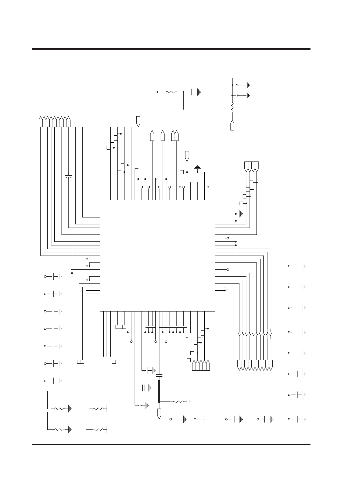
2) SPCA536 DSP
59
C112
104P
D3V3_DSP
T
27XTALO
RTCXTALI
RTCXTALO27XTALI
R97 33R
C100
20P
S
O
R0402
[10..0]
R98
C111
C110
C109
C108
C107
C106
C105
C104
C103
C102
C101
b
27XTALI
C0402
C0402
C0402
104P
104P
C0402
104P
C0402
C0402
104P
104P
C0402
C0402
104P
104P
C0402
C0402
104P
104P
C0402
C0402
104P
C0402
104P
[47..0]
B[9..0]
[47..0]
P
_CLK
EF
GPIO
D0
TX
D0
RX
R0402
1M
Y2
27M
A3V3_DSP
P1V8_DSP
RG
R0402
R101
100K
P
RESET
TRA
SP
JTAG_TRS
JTAG
JTAG_TM
JTAG_TDI
JTAG_TD
AUDP[5..0]
CHC
CHB
AGCOUT
OPO
A_VR
OPI
AGC
MICN
MICP
27XTALO
3K6
R0402
R100
R0402
R99 33R
C11320P
TGGPIO
TGGPIO
C0402
C122
C121
C120
C119
C118
C117
C116
C115
D3V3_DS
P1V8_D
D3V3_DSP
A3V3_DSP
D3V3_DSP
D3V3_DSP
RTCXTALO
R102 33R
C114 6P
104P
C0402
C0402
104P
C0402
104P
104P
C0402
104P
C0402
104P
C0402
C0402
104P
104P
C0402
AGND
R0402
12
C0402
TGGPIO1 TGGPIO2 TGGPIO3 TGGPIO4
TGGPIO31
TGGPIO30
TGGPIO29
TGGPIO28
TGGPIO27
TGGPIO26
TGGPIO25
TGGPIO24
TGGPIO23
TGGPIO22
TGGPIO41
TGGPIO42
TGGPIO43
TGGPIO44
TGGPIO36
TGGPIO47
RGB0
RGB1
RGB2
RGB3
RGB4
RGB5
RGB6
RGB7
RGB8
RGB9
TESTMODE
TGGPIO0
TGGPIO1
TGGPIO2
TGGPIO3
TGGPIO4
TGGPIO5
TGGPIO6
TGGPIO7
TGGPIO8
TGGPIO9
TGGPIO10
TGGPIO11
TGGPIO12
TGGPIO13
RESETb
TRAP
GPIO11
GPIO12
GPIO13
GPIO14
GPIO15
AUDP0
AUDP1
AUDP2
AUDP3
AUDP4
AUDP5
CHD
GPIO0
GPIO1
GPIO2
GPIO3
GPIO4
GPIO5
Y3
32.768KHz
C127
NC
C0402
TGGPIO33TGGPIO43 TGGPIO32
C0402
C126
NC
C125
NC
C0402
C0402
C124
NC
TGGPIO0
B3
C2
A2
A1
B2
D3
C3
D2
K3
H2
L3
G2
L4
E1
J3
J2
M4
F1
H4
G1
G4
H1
F3
K2
J1
G5
F4
L2
E3
K1
F5
L1
E5
M2
D5
M1
C5
N1
E6
N2
D6
ST
P1
C6
C7
M3
N5
N4
R1
P2
T1
U1
V1
N3
W1
P3
R2
P4
T2
P5
T3
CHD
Y1
CHC
R3
CHB
U2
W5
V2
R4
OPI
AA1
AGC
R5
W2
Y2
T5
AB1
AA2
T4
U3
V3
AB2
U4
RTC3V3
AB3
AA3
Y3
W3
AB4
V4
AA4
W4
V7
GPIO17
Y4
GPIO16
RTCXTALI
100S
XTAL-
6P
C0402
C123
C131
NC
C130NCC0402
C129NCC0402
C128
NC
RGB0
RGB1
RGB2
RGB3
RGB4
RGB5
RGB6
RGB7
RGB8
RGB9
OVDD6
OVSS6
PR
TRAP
DVDD5
DVSS5
OVDD7
OVSS7
AUDP0
AUDP1
AUDP2
AUDP3
AUDP4
AUDP5
AVDD2
AVSS2
OPO
A_VREF
MICN
MICP
XVSS1
XTALI
XTALO
XVDD1
XVSS2
XVDD2
OVDD8
OVSS8
GPIO0
GPIO1
GPIO2
GPIO3
GPIO4
GPIO5
TxD0
RxD0
C0402
C0402
TGGPIO0
TGGPIO1
TGGPIO2
TGGPIO3
TGGPIO4
TGGPIO5
TGGPIO6
TGGPIO7
TGGPIO8
TGGPIO9
JTAG_TDI
AGCOUT
XTALRTCI
TESTMODE
TGGPIO10
TGGPIO11
TGGPIO12
TGGPIO13
JTAG_CLK
JTAG_TMS
JTAG_TDO
XTALRTCO
V1/TGGPIO31
V2/TGGPIO30
V3/TGGPIO29
V4/TGGPIO28
V5/TGGPIO27
V6/TGGPIO26
V7/TGGPIO25
V8/TGGPIO24
V9/TGGPIO23
V10/TGGPIO22
ADCK/TGGPIO43
PBLK/TGGPIO44
JTAG_TRSTb
U7
ADCLP/TGGPIO41
OBCLP/TGGPIO42
FMGPIO1
0
C132
TGGPIO34FMGPIO3FMGPIO2
R106
CHDCHC
R105
R104
R103
MSHUTTER/TGGPIO36
FLASHCTR/TGGPIO47
FMGPIO0
FMGPIO1
V14
AB5
FMGPIO1
FMGPIO0
FMGPIO22
FMGPIO5
5
TP72TP7
TP7
NC
C0402
10K
R0402
R0402
NC/10K
10K
R0402
R0402
10K
FMGPIO2
FMGPIO3
AA5Y5AB6
FMGPIO2
FMGPIO4
FMGPIO3
FMGPIO25
FMGPIO27
FMGPIO26
8
TP7
D3V3_DSP
D3V3_DSP
FMGPIO4
FMGPIO5
AA6Y6AB7
W14
FMGPIO6
FMGPIO5
FMGPIO29
FMGPIO28
P1V8_DSP
E2
B1C1J4
DVSS4
DVDD4
FMGPIO6
FMGPIO7
FMGPIO7
FMGPIO8
FMGPIO31
FMGPIO30
TP82TP80TP83TP79TP81
D4
D3V3_DSP
F2
B4
OVSS5
OVDD5
FMGPIO8
FMGPIO9
Y7
AA7
FMGPIO10
FMGPIO9
FMGPIO33
FMGPIO36
4
P3V3_SYS
1SS355
12
R107
SOD323
D3V3_DSP
OVSS4
OVDD4
FMGPIO10
FMGPIO11
FMGPIO12
V5
AB8
FMGPIO11
FMGPIO12
FMGPIO38
FMGPIO37
0
2
TP89TP86TP8
TP9
TP9
1
1
1
TP9
RTC3V3
1K
R0402
R108
510R
R0402
TGGPIO37
TGGPIO38
TGGPIO39
TGGPIO34
C4A3E7
SEN/TGGPIO37
SCK/TGGPIO38
SDO/TGGPIO39
FMGPIO13
FMGPIO14
FMGPIO15
AA8
AB9
AB10Y8AB11
FMGPIO15
FMGPIO16
FMGPIO13
FMGPIO14
104P
C133
C0402
G_CAP
GC1
MC_621
12
TGGPIO35
TGGPIO33
TGGPIO40
TGGPIO32
B5D4A4
A5K5K4D1A6
FR/TGGPIO34
FH1/TGGPIO32
FH2/TGGPIO33
VSUBCTRL/TGGPIO40
FMGPIO16
FMGPIO17
FMGPIO18
FMGPIO19
Y9
W7
AA10
FMGPIO19
FMGPIO17
FMGPIO18
FMGPIO20
CHARGE RTC
BACKUP
POWER
TGGPIO21
TGGPIO46
TGGPIO20
TGGPIO45
B6
H3
FS/TGGPIO45
SUB/TGGPIO35
SG7A/TGGPIO20
SG7B/TGGPIO21
FCDS/TGGPIO46
FMGPIO20
FMGPIO21
FMGPIO22
FMGPIO23
FMGPIO24
Y10
W10
AB12
AA11
FMGPIO24
FMGPIO21
FMGPIO22
FMGPIO23
FMGPIO[42..0]
TGGPIO[47..0]
TGGPIO19
TGGPIO18
TGGPIO17
TGGPIO16
A8
B7H5A7
SG3A/TGGPIO16
SG3B/TGGPIO17
SG5A/TGGPIO18
SG5B/TGGPIO19
FMGPIO25
FMGPIO26
FMGPIO27
FMGPIO28
Y11
W11
AB13
AA12
FMGPIO25
FMGPIO26
FMGPIO27
FMGPIO28
R109
A3V3_DSP A3V3_DSP
C0402
3
TP9
TGGPIO15
TGGPIO14
C134 104P
ROUT
B10
B9B8A9
A10
ROUT
SG1A/TGGPIO14
SG1B/TGGPIO15
FMGPIO29
FMGPIO30
FMGPIO31
FMGPIO32
V8
W8
AA13
AA14
AB14
FMGPIO31
FMGPIO33
FMGPIO30
FMGPIO29
FMGPIO32
8K2
R0402
R0402
C0402
R110 150R
C135 104P
B11
A11
CBL
CBU
RSET
FMGPIO33
FMGPIO34
FMGPIO35
Y14
Y12
FMGPIO34
FMGPIO35
COUT
BOUT
C8
A12
B12
COUT
V_VREF
FMGPIO36
FMGPIO37
Y13
Y15
AA15
FMGPIO38
FMGPIO37
FMGPIO36
10uF/10V
C0805
10K/NC
10K
R116
R114
TGGPIO7
TGGPIO6
A3V3_DSP
TP124
10K
10K
R117
R118
TGGPIO9
TGGPIO10
1
22U
L7
SDR_CS
SDCLKn/DRGPIO3
MA14/DRGPIO2
MA13
MA12
MA11
MA10
MA9
MA8
MA7
MA6
MA5
MA4
MA3
MA2
MA1
MA0
CKE
UDQM
LDQM
UDQS/DRGPIO5
LDQS/DRGPIO4
MWEn
CASn
RASn
SDCLK
SDR_MD15
SDR_MD14
SDR_MD13
SDR_MD12
SDR_MD11
SDR_MD10
SDR_MD9
SDR_MD8
SDR_MD7
SDR_MD6
SDR_MD5
SDR_MD4
SDR_MD3
SDR_MD2
SDR_MD1
SDR_MD0
536_MD15
536_MD14
536_MD13
536_MD12
536_MD11
536_MD10
536_MD9
536_MD8
536_MD7
536_MD6
536_MD5
536_MD4
536_MD3
536_MD2
536_MD1
536_MD0
SDR_VCCQ4
SDR_VCCQ3
SDR_VCCQ2
SDR_VCCQ1
SDR_VCC3
SDR_VCC2
SDR_VCC1
SDR_VSSQ4
SDR_VSSQ3
SDR_VSSQ2
SDR_VSSQ1
SDR_VSS3
SDR_VSS2
SDR_VSS1
OVSS1
OVDD1
DVSS1
DVDD1
UVSS
DM
DP
UVDD
SUSPEND
UTMI30
UTMI29
UTMI28
UTMI27
UTMI26
UTMI25
UTMI24
UTMI23
UTMI22
UTMI21
UTMI20
UTMI19
UTMI18
UTMI17
UTMI16
UTMI15
UTMI14
UTMI13
10K
10K/NC
R119
RP1-1
TGGPIO12
TGGPIO14
B
C144
100uF/6V3
TANT-
+
AGND
1
L2520
+
C143
C1206
22uF/6V3
A22
TRAP
3
R21
R20
MA14
R22
MA13
R18
MA12
C20
MA11
1
T2
MA10
D19
MA9
2
T2
MA8
B20
MA7
9
T1
MA6
E17
MA5
U20
MA4
C18
MA3
U21
MA2
C19
MA1
U22
MA0
B21
CKE
B22
UDQM
8
T1
LDQM
E15
DRAMGPIO5
U19
DRAMGPIO4
V21
MWRb
C21
CASb
V20
RASb
D20
SDCLK
G2
34
1
47R
SMD15
56
2
F2
47R
SMD14
J2
34
2
47R
SMD13
12
K22
47R
SMD12
78
E21
47R
SMD11
D21
47R
SMD10
56
0
J2
47R
SMD9
M21
56
47R
SMD8
N22
12
47R
SMD7
M22
34
47R
SMD6
G2
0
SMD5
E20
SMD4
47R
L22
78
47R
SMD3
E22
SMD2
47R
78
H22
47R
SMD1
12
2
G2
47R
SMD0
V22
MD15
D18
MD14
V19
MD13
E18
MD12
U18
MD11
E19
MD10
W21
MD9
8
F1
MD8
W20
MD7
9
F1
MD6
W19
MD5
8
G1
MD4
V18
MD3
W22
MD2
Y21
MD1
Y20
MD0
R124
0R
R0603-S
J2
1
F2
0
K21
H20
0R
D17
R123
R0603-S
F2
1
P21
L21
N21
H21
D22
E16
C22
P20
G1
9
H18
H19
J18
J1
9
W18
V17
K18
TP
152
Y19
K19
150
TP
Y22
149
TP
K20
TP
148
AA21
L19
146
TP
AA20
L20
P19
M19
W17
M20
TP
140
AA22
NF_D0
N18
138
TP
AB22
N19
33R
136
TP
AA19
N20
W16
1 2
RP5-1
FMGPIO14
10K
10K
10K
10K
10K
10K
10K
10K
1 2
1 2
5 6
3 4
7 8
7 8
1 2
R120
R122
R125
R126
RP1-3 10K
RP1-2
RP1-4
RP6-4
RP6-1
RP11-1 10K
TGGPIO24
TGGPIO32
TGGPIO33
TGGPIO34
TGGPIO35
TGGPIO15
TGGPIO16
TGGPIO17
TGGPIO18
TGGPIO19
C142
DIGTV17
DIGTV20
2
P18
P22
OVSS2
DIGTV21
6
D3V3_DSP
R19
DVSS2
OVDD2
D3V3_DSP
0
1
TP12
P1V8_DSP
P3V3_SYS
T20
DVDD2
+
1
4
TP9
BOUT
C138
10uF/10V
C0805
+
P1V8_DSP
C136
104P
C0402
5
1
1
TP9
C137
22uF/6V3
C1206
+
AGND
R0402
R111
180K
AGND
E4
E10
AVSS1
GPIO6
A3V3_DSP
B14
GPIO6
AVDD1
GPIO7
C10
GPIO7
GPIO[10..0]
GPIO8
GPIO9
B13
A14
GPIO9
GPIO8
P1V8_SYS
GPIO10
A13
GPIO10
C11
D3V3_DSP
A16
OVSS3
OVDD3
P1V8_DSP
D14
C14
DVSS3
DVDD3
DIGTV20
DIGTV21
A15
B15
DIGTV21
DIGTV15
DIGTV19
A17
DIGTV20
DIGTV19
C139
DIGTV18
DIGTV17
B16
C13
DIGTV18
104P
DIGTV17
C0402
DIGTV16
DIGTV15
A18
D13
DIGTV16
DIGTV13
DIGTV14
C15
DIGTV15
DIGTV14
DIGTV12
B17
DIGTV13
DIGTV11
A19
C12
DIGTV12
DIGTV[21..0]
DIGTV9
DIGTV10
B18
C16
DIGTV11
DIGTV10
DIGTV8
C17
DIGTV9
GPIO9
FMGPIO2
4
TP24
DIGTV6
DIGTV7
D15
A20D9B19C9A21
DIGTV8
DIGTV7
FMGPIO3
TP96TP10
DIGTV5
DIGTV6
FMGPIO40
FMGPIO39
0
8
TP9
DIGTV3
DIGTV4
DIGTV5
DIGTV4
GPIO6
TP102TP114TP11
TP108TP11
DIGTV1
DIGTV0
DIGTV2
D16
E14
DIGTV3
DIGTV2
DIGTV1
DIGTV0
DIGTV16
0
TP11
SPCA536A_MCM
OVDD9
OVSS9
DVDD6
FMGPIO38
FMGPIO39
FMGPIO40
Y16
AB15
FMGPIO39
FMGPIO40
FMGPIO41
FMGPIO42
AA16
AB16
FMGPIO42
FMGPIO41
NF_D0
E9
E13
NF_D0
NF_D1
NF_D[7..0]
NF_D1
D12
NF_D2
NF_D2
D11
NF_D3
NF_D3
NF_D4
NF_D4
NF_D5
NF_D6
NF_D7
NF_VSS1
J5
E8
D7
G3
W13
NF_D6
NF_D5
NF_D7
NF_VSS2
D10
NF_VCC1
D8
W12
D3V3_NF
R0402-S
R112 0R
D3V3_DSP
NF_VCC2
U5
R113 10K
NF_SEb
R0402
W6
DVSS6
V9
P1V8_DSP
V6
W9
AA9
D3V3_DSP
OVDD10
OVSS10
V13
D3V3_DSP
UTMI0
UTMI1
UTMI2
UTMI3
UTMI4
UTMI5
UTMI6
UTMI7
UTMI8
UTMI9
UTMI10
UTMI11
V16
AB18
107TP111
TP
C141
C140
UTMI12
V15
V10
Y18
10K
AA18
AB19
AB20
AB21
115
113TP118
5 6
TP
TP
C0402
104P
C0402
104P
RP11-3
TGGPIO25
Y17
W15
AB17
AA17
9
101
TP
TP9
D3V3_NF
DRAMGPIO
TP165
TP
164
163
TP
TP
162
161
TP
160
TP
159
TP
TP158
R129
R128 47R
R127
R130
P
D3V3_SDRAM
D3V3_DSP
P1V8_DSP
DM
DP
D3V3_DSP
D3V3_SDRAM
NF_D3
NF_D1
NF_D4
NF_D2
33R
33R
33R
33R
5 6
3 4
7 8
R133
RP5-3
RP5-2
RP5-4
FMGPIO17
FMGPIO15
FMGPIO18
FMGPIO16
10K
10K
10K
10K
3 4
7 8
5 6
3 4
RP6-2
RP6-3
RP11-2
RP11-4
TGGPIO46
TGGPIO42
TGGPIO44
TGGPIO45
MA[14..0]
RP4-2
RP4-3
RP3-2
RP3-1
RP4-4
RP3-3
RP2-3
RP2-1
RP2-2
RP2-4
RP3-4
RP4-1
D3V3_DS
C152
C151
C150
C149
C148
C147
C146
NF_D5
NF_D7
NF_D6
33R
33R
33R
R136
R135
R134
FMGPIO19
FMGPIO20
FMGPIO21
R73 10K
R72 10K
TGGPIO36
TGGPIO11
DRAMGPIO4
MD15
MD14
MD13
MD12
MD11
MD10
MD9
MD8
MD7
MD6
MD5
MD4
MD3
MD2
MD1
MD0
C0402
104P
104P
C0402
C0402
104P
104P
C0402
C0402
104P
C0402
104P
C0402
104P
Page 59
60
Ⅵ. CIRCUIT DIAGRAM
60606060
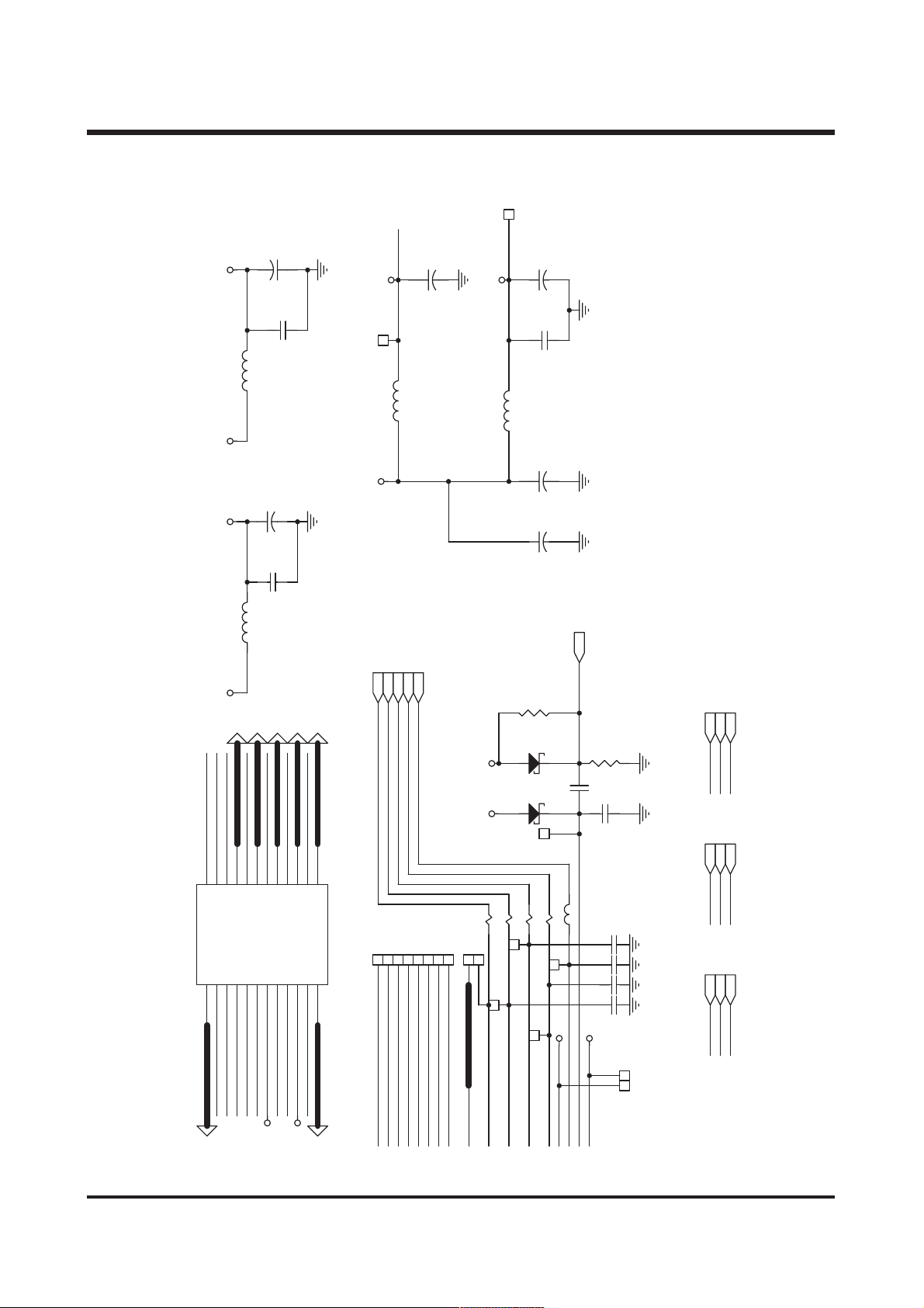
3) IMAGESENSOR-RPERIPHERIC CIRCUIT
D3V
R62
100K
R0402
C60
104P
C0402
XI
R261
NC
NC
C199
CCD_V5A
CCD_V5B
CCD_V6
CCD_V6
CCD_V5B
CCD_V5A
D3V
D3V
D3V
D3V
CCD-VL
D3V
D3V
NOESHUT
CCD_V3A
CCD_V4
CCD_V3B
CCD_V3A
CCD_V4
CCD_V3B
C46
104P
C0402
C45
104P
C0402
C44
104P
C0402
C0402
C43
104P
C0402
C42
104P
C41
104P
C0402
C195
104P
C0402
R58
R57
CCD_V2
CCD_V1
CCD_SUB
CCD_V1
CCD_V2
+
C47 1u/25V C0603
100K
R0402
100K
R0402
CCD_SUB
IV2
IV1
IV3
1
CH1
IV4
1
1
TP47
CH4
D3V
CCD-VL
CCD-VH
1
TP49
STO STB
TP303
BGA-NN12062A
C10
D13
A8
E13
M3
L12
M13
N10
L8
N8
N4
N7
N6
G13
VL
K1
VL
H13
M2
H12
F3
J1
A11
C6
A5
V6
F2
V4V3CH4V5CH5
U4
G2
IV4
100K
R60
R0402
100K
R59
R0402
VH
IV3
IV2
IV1
VM
VM
IV3
IV4
IV6
G1
TP301
1
OV1
OV2
OV3
OV4
OV5
OV6
OV7
OV8
VDC
VHH
CH3
ICH4
ICH2
ICH1
OSUB
ICH3
C8
CH2
1
TP300
1
CH3
CH3
D3A1D1
CH4
1
1
302
TP
1
CH2
1
TP45
CH2
1
1
TP31
1
CH1
1
TP46
CH1
1
1
TP32
1
IV2
IV1
1
V2
SUB
E1J2K3
1
1
TP33
V1
VSS
CCD_SUBCTRL
1
D3V
DVSS2
SUBSW
SUBSW2
VDD
EXADCLK
EXDS2
L1L2L3N3L4M4L5
K2
A3V
C49
C48
33P
DVSS3
DVDD2
EXDS1
VSS
105P
C51
C50
NC
NC
C0402
C0402
CCD_H2
CCD_H1
CCD_HL
CCD_FR
CCD_H1
D3V
H1
DVDD3
CCD_HL
D3V
DVSS3
DVDD3
CCD_FR
R
HL
CCD_H2
D3V
H2
DVDD3
DVSS3
NN12062A
DC_DET1
DC_DET2
VDD
CCDOUT
DC_DET3
VDD
DC_DET4
VSS
AUX
L6M6L7
N5
M5
105P
C52
A3V
C0402
C0603
C53 104P/25V
CCDIN+
CCDIN+
105P
C54
A3V
D3V
104P
C55
104P
C56
R63
C57
104P
C58
104P
CLR
CDS_ADCCLK
8
TP18
1
D3V
D3V
DVDD2
DVDD3
VRB
VRT
L9
M7
M8
104P
C59
D3V
173
TP
R0402
1K2/NC
C0402
1
CLR
C9B9A9B8C7A7B7A6B6B5C4A4B4A3B3D2F1E2E3H2J3H3H1G3C2
CLR
CLKO
DVDD1
DVSS1
N9
M9
TP178
1
TP174
1
D3V
XI
XO
B10
A10
XI
XO
TEST2
NOE
STBCSDATA
L10
M10
1
TP182
1
TP227
1
1
TGGPIO37
1
CDS_SEN
NOE
STB
C61
D3V
A13
B11
TEST1
CCDSW1
CCDSW2
HD
VD
STO
SHUT
DVDD2
DVSS2
DRVSS2
D9
D8
D7
D6
D5
D4
DRVDD
D3
D2
D1
D0
NC
NC
DCLK
N11
M11
1
1
1
TGGPIO38
TGGPIO39
CDS_SDI
CDS_SCK
C0402
104P
C11
C12
C13
D12
D11
E12
E11
F12
F13
F11
G12
G11
H11
J13
J12
J11
K13
K12
K11
L13
L11
D3V
33R
R65
48MHZ
CDS_CLCCD
TP200
1
197
TP
D3V
D3V
33R
33R
12
34
RP7-1
RP7-2
CDS_D1
CDS_D0
C63
104P
C0402
HDVDSTO
TP216
1
TP205
1
1
33R
33R
56
12
RP7-3
RP8-1
CDS_D2
SHUT
1
1
1
33R
33R
78
34
RP7-4
RP8-2
CDS_D5
CDS_D4
CDS_D3
D3V
1
33R
33R
78
56
RP8-4
RP8-3
CDS_D7
CDS_D6
C66
33R
33R
R76
R77
CDS_D8
CDS_D9
104P
C0402
CCD-VL
CCD-VL
A3VA3V CCD-VH CCD-VH
A3V
D3V
C75
C196
C72
C71
C70
C69
C68
C67
104P
104P
104P
104P
104P
104P
104P
104P
C0402
C0402
C0402
C0402
C0402
C0402
C0402
C0402
Page 60
61
Ⅵ. CIRCUIT DIAGRAM
616161
3-1) IMAGESENSOR-RPERIPHERIC CIRCUIT
61
22uF/16V
TANT-B
C87
+
A3V
C0402
C89
104P
1
TP51
A3V
1
TP61
1
D3V
C92
22uF/10V
+
C93
104P
C0805
C0402
C90
22uF/10V
C0805
+
1
D3V
P12V_CCD CCD-VH N8V_CCD CCD-VL
CCD_V2
CCD_V1
CCD_V3A
L2520
L3 0R
C86
+
C88
L2520
L4 0R
CCDIN+
CCD-HL
22uF/16V
TANT-B
C0402
104P
CCD-H2
CCD-H1
L2520
L5 22U
P3V3_CCD
CCD_H1
CCD_H2
CCD_HL
CCD_H1
CCD_HLCCD_V6
CCD_FR
CCD_FR
CCD_SUBCTRL
CCD_SUBCTRL
L6 0R
CCD-VH
D3V
L2520
R93
D3
1SS355
D2
1SS355/NC
C91
10uF/10V
+
C202
100uF/6V3
+
R0402
100K
SOD323
12
SOD323
12
1
TP64
C0805
TANT-B
1
CCD_SUB
CCD_SUB
C0402
R96
104P
C198
C94
R0402
NC/100K
C0402
102P
CCD_V5A
CCD_V5B
CCD_V6
CCD_V5A
CCD_V5B
CCD_V6
CCD_V3A
CCD_V3B
CCD_V4
2
CCD_V3A
GND
CONN2
1
8196
4
GND
CCD_V1
CCD_V2
CCD_V3B
CCD_V4
CCD_V5A
357
CCD_V5A
CCD_V3B
CCD_V4
CCD_V5B
102114131822
9
12
16
GND
GND
CCD_HL-8V
CCD_OUT
SUB
CCD_V5B
CCD_V6
151723
11
CCD_V6
CCD-SUB
CCD-VL
20
GND
CCD_H2
CSUB
+12V
CCD-SUBCTRL
CCD-VH
24
GND
CCD_H1
GND
CCD_RG
FPC2X12_M_PTH0.4
CCD-RG
TP59
TP58
1
1
1
1
CCD_V5B CCD_H2
TP57
TP56
TP55
1
1
1
1
1
1
CCD_V5A
CCD_V4
CCD_V3B
TP52
TP54
TP53
1
1
1
1
1
1
CCD_V3A
CCD_V2
CCD_V1
0R
R90
TP50
TP34
1
1
1
1
CCD-HL
CCDIN+
1
TP60
0R
0R
R92
R91
1
TP62
1
TP63
CCD-H1
CCD-H2
1
1
0R
R94
TP65
CCD-RG
L0603
0R
B3
1
1
CCD-VL
CCD-VH
1
CCD-SUBCTRL
CCD-SUB
C96
C97
C95
1
1
33P
33P
C0402
C0402
1
1
CCD_V3A
CCD_V3B
CCD_V4
CCDIN+
100P
C98
TP68
TP67
C0402
33P
C0402
CCD_V1
CCDIN+
CCD_V1
CCD_V2
SENSOR CON
CCD_V2
Page 61
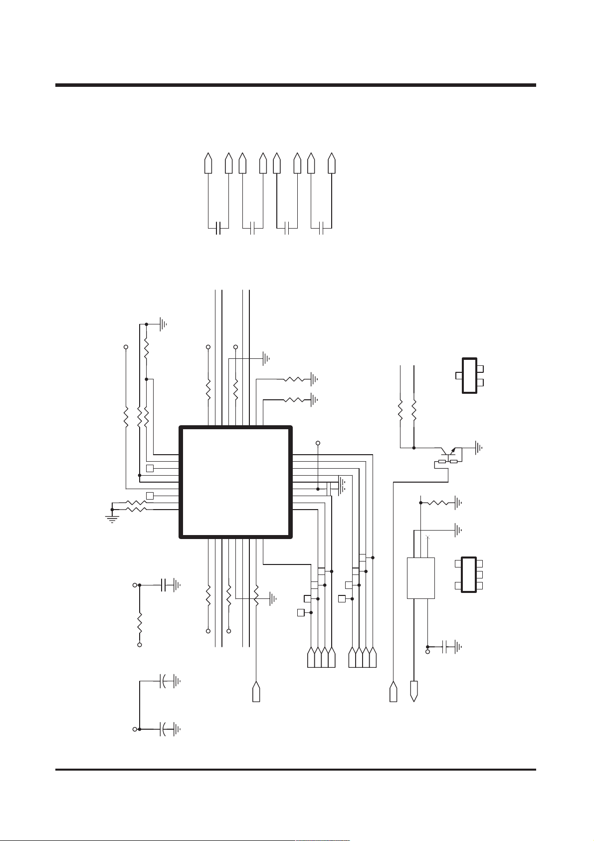
62
Ⅵ. CIRCUIT DIAGRAM
62626262
3-2) IMAGESENSOR-RPERIPHERIC CIRCUIT
AF_O1A
AF_O1B
AF_O2A
AF_O2B
IRIS_O1
IRIS_O2
IRIS_O3
IRIS_O4
R79
10K
O
P4V_MOT
0R R0402-S
RS3
R80 2R R0402
R0402
R78
10K
O-S
P3V3_MOT
R0402
R82 11K
R0402TP37
R81 25.5K
1
1
TP36
R0402
R0402-S
1
1
C78
10u/10V
19
20
21
22
23
24
25
26
27
U5
C0805
AF_O1B
AF_O1A
C80
104P
C0402
O-S
IRIS_O3AF_O1B
IRIS_O4
P3V3_MOT
R0402
R84 10K
15
16
17
18
SEL2
OUT4A
OUT4B
IN5
VLIM
VREF
RNF
VM3
EN1
PGND2
OUT5A
SENSE
OUT5B
SEL1
OUT1A
OUT1B
VM1
282930313233343536
R0402
RS6 0R
R83 10K
AF_O2A
C81
O
IRIS_O2
IRIS_O1
P4V_MOT
R0402-S
RS7 0R
12
13
14
VM2
OUT3B
BD6758KN
PGND1
OUT2A
R0402-S
AF_O2B
C0402
104P
10
11
BRK1
BRK2
OUT3A
OUT2BPSIN1A
R0402-S
RS8 0R
IRIS_O1
C83
104P
R86
R85
IN4B
IN4A
IN3B
IN3A
GND
VCC
IN2B
IN2A
IN1B
IRIS_O2
C0402
R0402
100K
R0402
100K
QFN-36P
9
8
7
6
5
4
3
2
1
TP221
8
1
4
TP21
1
TP30
IRIS_O3
C84
104P
O-S
P3V3_MOT
1
TP222
1
1
1
IRIS_O4
C0402
C82
104P
1
1
TP224
1
TP223
C0402
1
TP225
1
1
Q2
DTC143XUA
3
4.7K
2
100K
R0402
SN74LVC1G14
SOT-25_0.65
3
2
SOT-23-B
3
SOT323_UMT
1
10K
45
123
SOT-23-5
AF-C
AF-E
R0402
R0402
R88 10K
R87 220R
R89
AF-E
1
1
1
TP226
1
1
1
2
A
NC
GND
VCC
Y
U6
5
43
RS4 0R
P3V3_SYS
O
P4V_MOT
C77
10u/10V
+
C76
100u/6V3
+
C0805
TANT-B
O
AF_O1A
O-S
P4V_MOT
P3V3_MOT
AF_O2A
AF_O2B
GPIO2
GPIO1
GPIO0
AF_IN2
AF_IN1
N
MOTO_E
GPIO3
AF_IN4
AF_IN3
DIGTV18
DIGTV19
DIGTV20
DIGTV21
IRIS_IN1
IRIS_IN2
IRIS_IN3
IRIS_IN4
GPIO7
N
MOTO_E
O-S
TGGPIO12
P3V3_MOT
AF_HOME
C85
104P
C0402
Page 62
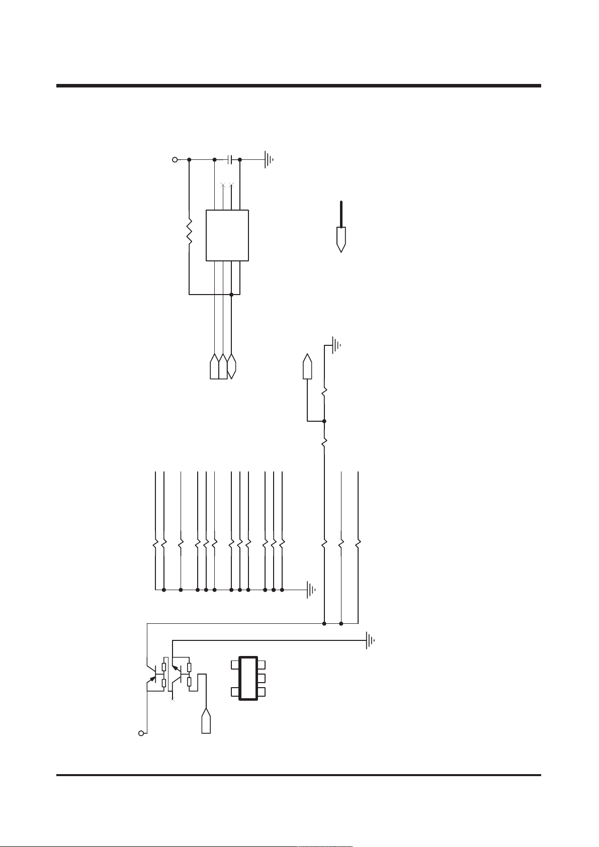
63
Ⅵ. CIRCUIT DIAGRAM
636363
4) TRAP/EEPROM
63
C28
104P
C0402
P3V3_SYS
876
5
R0402
NC
VCC
GND
ORG
AT93C66
CSSKDI
123
DO
4
R22 100K
U2
EEPROM
TGGPIO20
TGGPIO38
TGGPIO39
SOP-8
4.4*3 mm
ORG=HI/OPEN 16BIT
ORG=LO 8BIT
MA[14..0]
ISP
MA1
MA0
100K
100K
R21
R20
SOT-25_0.65
UMC2N
IO-TRAP
Q1
15
22k
3 4
MA2
10K
R23
MA3
10K
R24
22k 22k
22k
MA4
10K
R25
EE_CS
MA5
10K
R26
2
EE_SCK
EE_SDI
MA7
MA6
MA8
100K
10K
10K
R29
R27
R28
45
MA13
MA14
10K
R30 10K
R31
123
SOT-23-5
MA12
10K
R32
R0402-OP
R267 OR
10K
R0402
R34
MA11
MA9
100K
R36 10K
R33
PUT
TOPLAYER
MA10
10K
R35
256M H H L
MA9 LOAD PROGRAM TO LO
NORMAL TO HI
P3V3_SYS
TRAP
Page 63
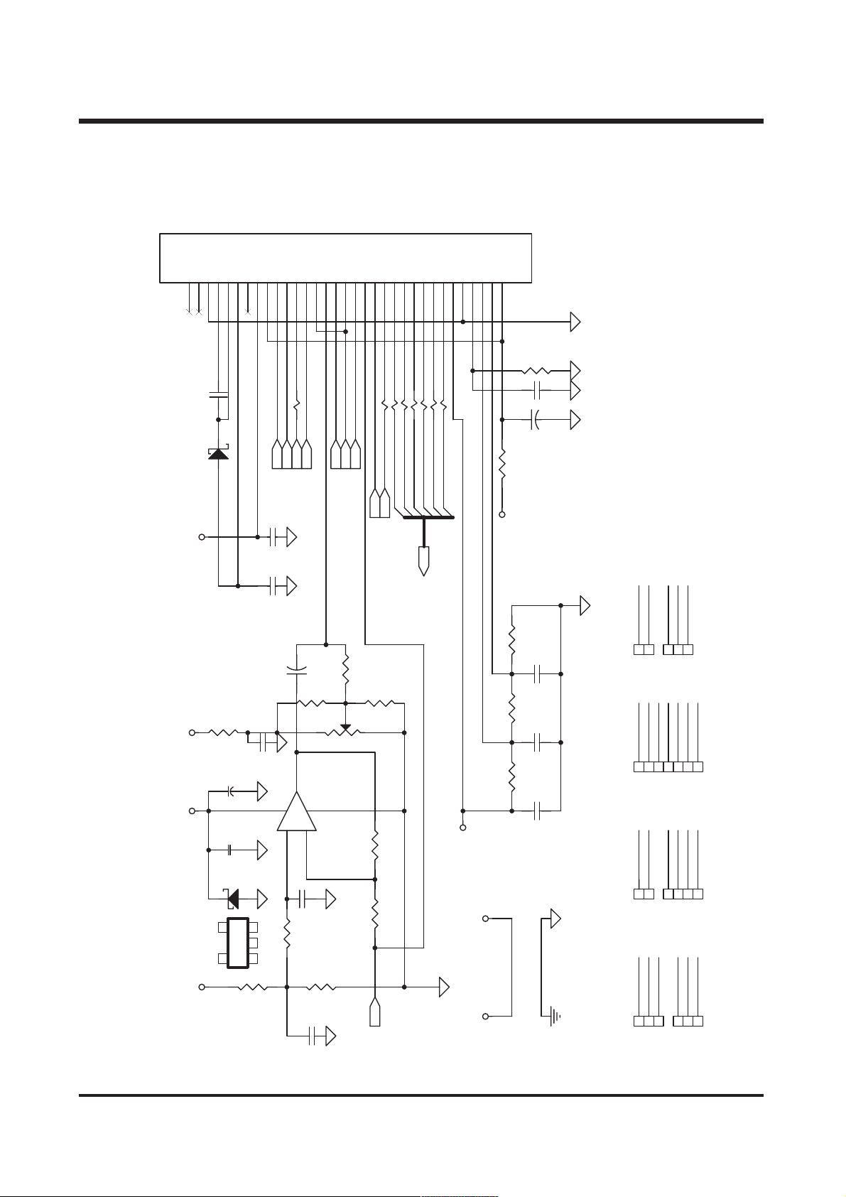
64
Ⅵ. CIRCUIT DIAGRAM
64646464
5) TFT LCD
N15V+/-1V
P15V+/-1V
0~7V5(P-P)
0V5~4V5
P5V+/-0V53VP3V~3V6
0V5~4V5
TFT1
NCNCVSS
VC1
VC2
VGLNCVGH
VDDCPGRES
GPCK
GSRT
STBYB
VCOM
STH
STBYB
RIT
POL
STB
CLK
D05
D04
D03
D02
D01
D00
VSH
123456789
5
4
105P
C0603
C29
12
D1
SOD323
RB501V-40
FT
P15V_T
N15V
TP15V_TFT
30K
R0402
R37
A5V_TF
C208
+
C210
10uF/16V
TFT COM20T2123 2.0 240(V)*354(H)
ZD6
12
45
T
A5V_TF
1011121314151617181920212223242526272829303132
11
10
TFT_CP
TFT_GRES
C0603
105P
C0805
2u2/16V
C33
10uF/16V
R0402
C0402
+
1
2V3
R39 10K
14
15
12
33R
R40
T
TFT_GSR
TFT_GPCK
-0.9+4V5
+
C0805
NC
3V4
4
-
3
NJM2125F
2V3
C34
104P
R0402
R41
19K1 1%
C35
104P
16
H
TFT_ST
10K
VR1
2 5
A
SOT-25_0.95
C0402
R0402
C0402
18
17
19
TFT_RIT
TFT_STBY
R0402
R42
R269
2
20K
21
20
33R
12
RP12-1
B
TFT_CLK
TFT_ST
NC
R0402
2
MVR2
1 3
R0402
R44 18K 1%
10K 1%
R0402
R43
L
TFT_PO
22
33R
34
33R
R46
RP12-2
TFT_D4 23
TFT_D5
8306
R268
B
22uF/16V
TANT-
C0805
15V
SOD323
123
SOT-23-5
R38
22K
9
C32
C31
C30
104P
U3
R0402
26
25
27
24
33R
33R
56
33R
33R
R48
R50
RP12-3
RP12-4
TFT_D1
TFT_D313TFT_D2
TFT_D0
TFT_D[0..5]
28
78
VSS
VSC
VRH
31
1V88
4V7
T
A5V_TF
TP5V_SYS
A5V_TF
VDD
VRL
33
33
32
R52 220R
P3V3_SYS
0V28
FPC-SJ032076-33P
+
C36
R0402
13uA
R0402
R55 3K1%
C39
R0402
R54 47K
C38
R0402
R53 3K1%
C37
4mA
105
104P
104P
104P
R56
C40
C0603
C0402
C0402
C0402
220K
104P
R0402
C0402
273026
32
31
18TP22TP26
10
6
TP
TP
TP
19202122232425
1
5
7
5
9
TP
1213151617
4
TP
456910
3
TP
TP2
TP13TP
TP1
TP2
16TP20TP24
8
TP
TP
0
3
7
TP3
TP2
TP11TP
9
TP2
18
28
TP
11
7
TP2
Page 64
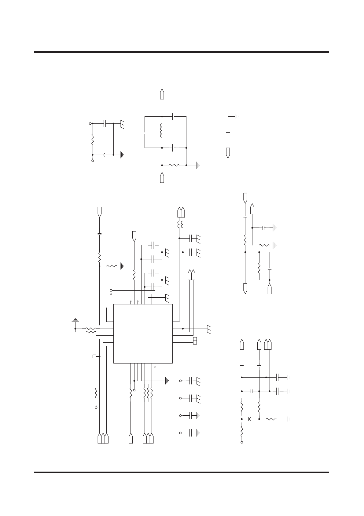
65
Ⅵ. CIRCUIT DIAGRAM
656565
6) USB1.1/MIC/TOOUT/BUZZE
65
C3
10uF/10V
C0805
A3V3_AVV
R0603-S
B
R3 0R
C2
100uF/6V3
TANT-
+
P3V3_SYS
C0402
C4 22P
VIDEOVIDEO_OUT
C0402
C10
330P
0R
L0805
L1
C9
270P
C0402
R12
100R
R0402
TV Out
C0805
C18 10uF/10V
A_VREF
AGCOUT
C19 104P
MIC
R14 1K
C20 104P
R15 10K
OPI
MICP
C0402
R0402
R0402
AGC
C0402
R0402C22
102P/NC
C21
100uF/6V3
+
249K 1%
R17
C23 104P
C0402
B
R16 1K
TANT-
C24
R18
R0402
MICN
C0402
R0402
1uF/16V
C0805
R0402
470K
C0402
C25 330P
OPO
MIC+
MIC-
R19
750R
MICPHONE
C27NCC0402
C26
NC
C0402
R0402
BUZZER
RIN1
LIN1
CSB
SDIN
SCLK
MONO-
MONO+
MODE
R0603-S
R7 0R
GPIO15
HP_DET
HP_DET
R0402-S
VREF
R8 0R
24
NC
NC
HP-D
VMID
VREF
WM8751
MCLK
DCVDD
DBVDD
DGND
BCLK
1234567
R0402-S
R0402-S
R10 0R
R9 0R
P3V3_AVV
0
2
AUDP0
AUDP2
C8
104P
C7
10u/10V
C6
104P
C5
10u/10V
17181920212223
AVDD
AGND
HPVDD
DACDAT
DACLRC
NC
8
R0402-S
R11 0R
1
AUDP1
C0402
C0805
C0402
C0805
C0402
C1 102P
R0402
R0402
R6
3K9
R5 10K
TO
P4V_MO
A3V3_AVV
VREF
25
1
R0402
R4 10K
P3V3_AVV
26
27
28
29
30
31
32
1
U1
TGGPIO39
TGGPIO38
QFN-32P
R2
10K
R0402
R1
10K
R0402
5
TP30
0R
SPKLOUT2
16
SPKROUT2
15
HPGND
14
HPLOUT1
13
HPROUT1
12
OUT3
11
MONO_O
10
AGND2
9
TO B1
P4V_MO
A3V3_AVV
P3V3_AVVP3V3_AVV
SP+
SP-
0R
B2
C0402
C16
100P
C0402
C15
100P
HP_L
HP_R
HPL
HPR
12/13 AU_O
1
SP1
1
1
SP2
1
C0402
C14
104P
C13
104P
C0402
C0402
C12
104P
C11
104P
C0402
AU_DA
AUDP5
AU_CK
MCLK
AUDP2
AUDP0
AUDP1
R13 750R
A3V3_DSP
Page 65
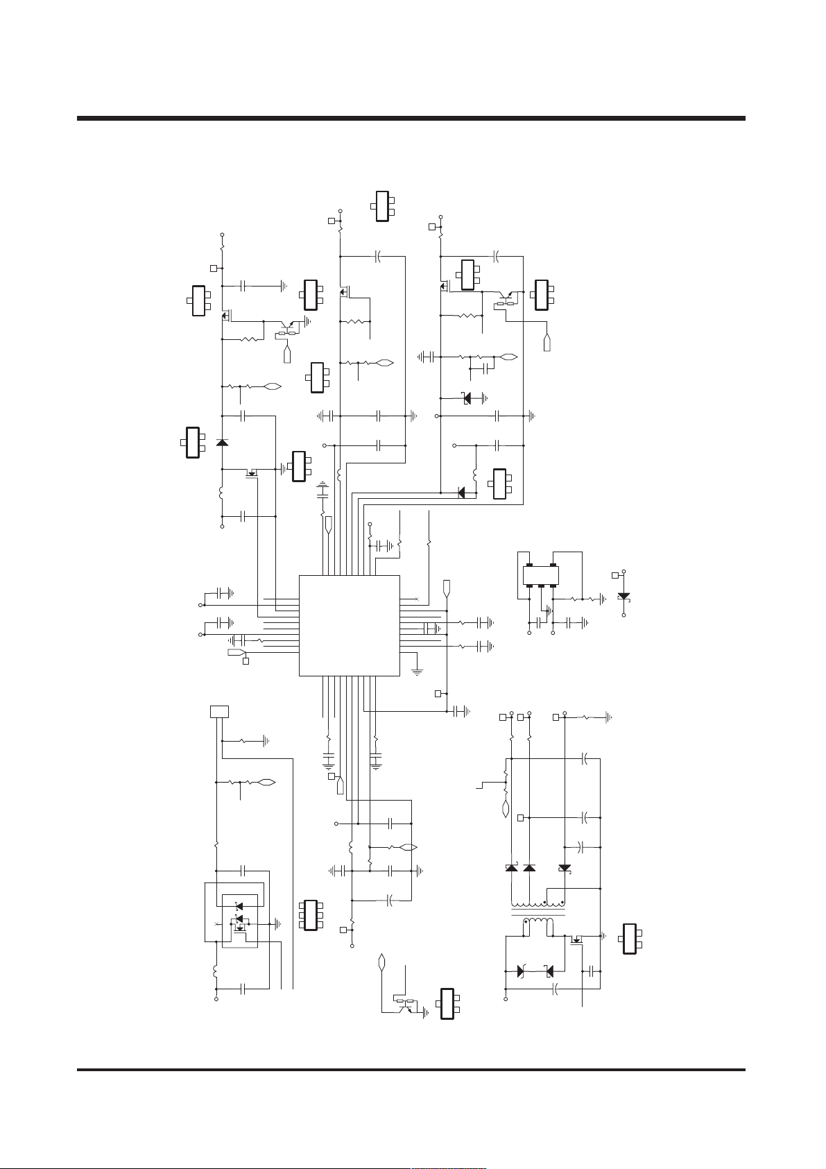
66
Ⅵ. CIRCUIT DIAGRAM
66666666
7) POWER MODULE-AT1388
3
3
SOT-23-A
P5V
P5V
O
CH-2
P4V_MOT
RS10 0R
1
170
1
TP
32
12
SOT-23-A
Q3
AO3413
STEP-UP
12
D5 SBS004
1 3
L9 6u8H
T
BAT
104P
C154
104P
C153
J1
2
1
TFT+
TFT-
0.7V
8+0.7V
0R
RS9
26
6
Q4
5
AO6702 SOT-
4
L8 22uH
STEP-UP
P5V_SYS
CH-3
R0603-S
1
R138
1.25V
3
SOT-2
C0402
C0402
TFT_BL_ON
LED_BL
R137
3
SOT-2
C0805
10uF/10V
C160
100K
R140
90.9K 1%
R142
200K 1%
FB2
C159
C0805
NC
Q5
AO3400
32
1
C158
C0805
10uF/10V
C0402
C157
R143
103P
1
1
TP228
CON1X2-DIP
R139
10R 1%
R141
90.9K 1%
787K 1%
FB3H
C156
22uF/10V
C1206
C155
C0805
10uF/10V
R0402
3
SOT-2
22K
FB2
1
2
3
3
4.7K
NGND
DL3
DL1
FB3L
Q6
NGND
DL3
3
3
1
DTC143XUA
SOT323_UMT
10K
2
PWR_ON
3
SOT-23-A
QFN-40P
31
32
33
34
35
36
37
38
39
3
40
U9
0.2V
4
56
FB3L
171
1
CH-M
TP
Q7
12
SOT-23-A
STEP-DOWN
1
3
2
SOT-23-B
C206
103P
P5V
12
C0402
222P
C161
10K
PWR_ON
R144
30
CC2
ON2
FB2
INDL2
GND
DL2
DL3
DL1
PV
CC3
FB3L
ON
FB3H
CC1
123456789
FB3H
FB1
10K
R145
C162
1
229
TP
P5V
123
SOT-23-6
P3V3_SYS
3
1
0R
R0603-S
RS11
1.25V
C164
+
3
32
SOT-2
AO3413
1
100K
R0402
R146
SDOKB
R150
90.9K 1%
R147
150K 1%
PWR IC
FBM
C167
C0402
C166
4u7H
L10
P5V
51K
R149
LXM
PVM
OSC
PGM
LXSU
PVSU
PGSU
MAX1566
FB1
ON1
PGSD
LXSD
PVSD
ONSD
FBSD
33K
R151
C0402
C163
222P
1
1.25V
CCD_ON
PWR IC
40.2K 1%
L11 10uH
R148
C207
C0402
103P
0R
RS12
1
R0603-S
1
TP172
P1V8_SYS
STEP-DOWN
CH-SD
C165
212223242526272829
SDOKB
CCSD
10
NGND
1
2
SOT-23-B
C1206
22uF/6V3
C0805
22uF/10V
C0805
10uF/10V
100P
C0402
AUX1OKB
SCF
ONSU
FBSU
CCSU
REF
ONM
FBM
CCM
SUSD
C0402
682P
C170
90.9K 1%
R152
C169
+
C168
NGND
4.7K
3
NGND
SDOKB
0R
RS13
10uF/10V
C0805
C0805
10uF/10V
C1206
22uF/6V3
PWR_ON
2
20
19
18
17
16
15
14
13
12
11
Q9
P5V_SYS
232
1
CH-SU
1
TP
0R
RS15
32
23
AO3413
Q10
SOT-
STEP-UP
PWR IC
C203
C0402
103P
P5V
T
BAT
D6
SCF
0R/NC
RS14
C0402
PWR_ON
C171 104P
FBSU
FBM
230
1
1
TP
PWR IC
NGND
3
DTC143XUA
SOT323_UMT
10K
3
SOT-23-B
1
R0603-S
3
1
R153
1.25V
ZD5
6V
SOD323
12
SBS004
R155
R154
C205
103P
1
2
SOT-23-A
R156
274K 1%
FBSU
3
L12
SOT-2
33K
33K
C0402
12
R0402
100K
SCF
R157
C209
6u8H
1 3
C173
C172
1.25V
C174
+
3
Q11
4.7K
90.9K 1%
NC
C0402
C176
C175
3
SOT-23-A
C0402
103P
C0402
682P
TP15
R159
FB1
R158
T1
2171
ST-
FLYBACK
CH-1
B
TANT-
100uF/6V3
3
1
DTC143XUA
SOT323_UMT
10K
2
NGND
C0805
22uF/10V
C0805
10uF/10V
12
U10
12mA
92mA
T
176
P15V_TF
TP
1
1
1
0R
RS16
RS17
1M 1%
90.9K 1%
1
175
TP
NGND
SOD323
12
RB501V-40
SBS004
D8
D7
5
T-N8_P3V3_P15
4
ZD3
3.9B
T
BAT
3
SOT-23-B
PWR_ON
5
SH
INGOFB
123 4
T
C177
C0402
104P
P15V_TF
P3V3_CCD
1
0R
1
23
SOT-
1 3
6
7
2
3
D9
SOD323
12
12
C178
1
2
SOT-25_0.95A
C197
P12V_CCD
1.5mA
177
N8V_CCD
TP
1
12
D10RB501V-40
8
1
32
SOD323
RB501V-40
B
100uF/6V3
TANT-
AT1202
1
R161
104P
1.24V
110K/NC
C0603
22uF/16V
C181
+
C180
+
C179
SOD323
Q12
AO3400
1
DL1
R162
R160
C1206
22uF/10V
22uF/10V
+
3
SOT-2
C182
12K/NC
10K
C0805
C0805
<AO3416>
C0603
0.15uF/16V/NC
TP306
1
12
ZD4
3
1
SOD323
3V9/NC
T P12V_CCD
P15V_TF
12
SOT-23-A
Page 66
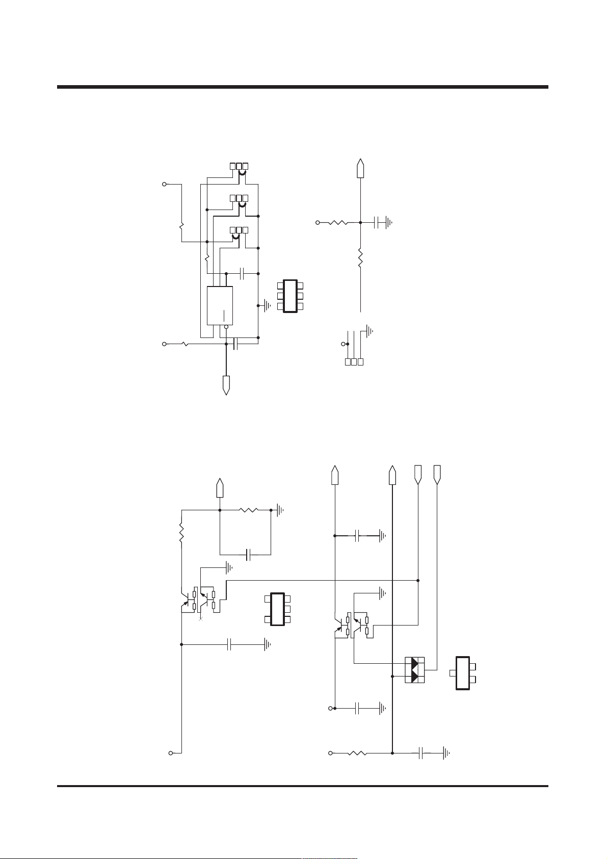
67
Ⅵ. CIRCUIT DIAGRAM
676767
8) POWER SOURCE/RESET/LED
67
P1V8_SYS
R0402-S
RS18 0R
U11
Power ON Reset
P3V3_SYS
R164
1K
R0402
213
3
2
1
3
2
1
R0402-S
C184
104P
VS2GND
RST VDD
RESETb
DS9801
C204
26
SOT-
105P
C0402
** PRESET 1V6 **
U11
4
56
123
SOT-23-6
RS19 0R
VS0 VS1
1 65234
R169
P3V3_SYS
4K7
BATT
R0402
LI_TMP
1
D
TEMP_A
C188
104P
C0402
R0402
R171 1K
P
LI_TM
3
2
LBAT
IN: 4V2~1V4
R0402
R163 13K7 1%
SOT-25_0.65
15
UMC2N
Q13
22k
3 4
(1.76~0.6V)
OT:1V76~0V59
D1V8~D2V0
22k 22k
22k
2
C183
22u/10V
C1206
R168
10K 1%
C185
104P
R0402
C0402
45
POWER SOURCE
4V2~1V5
BATT
123
SOT-23-5
PWR_ON
SOT-25_0.65
Q14
UMC2N
3 4
P5V
P3V3_SYS
C187
15
22k
C186
R170
104P
104P
22K
C0402
22k 22k
22k
C0402
R0402
PWR_DET
TGGPIO22
2
2
1
PWR_KEEP
3
D11
DAN202U
SOT-323_UMT
C189
104P
3
C0402
PWR_SW
3
12
SOT-323
Page 67
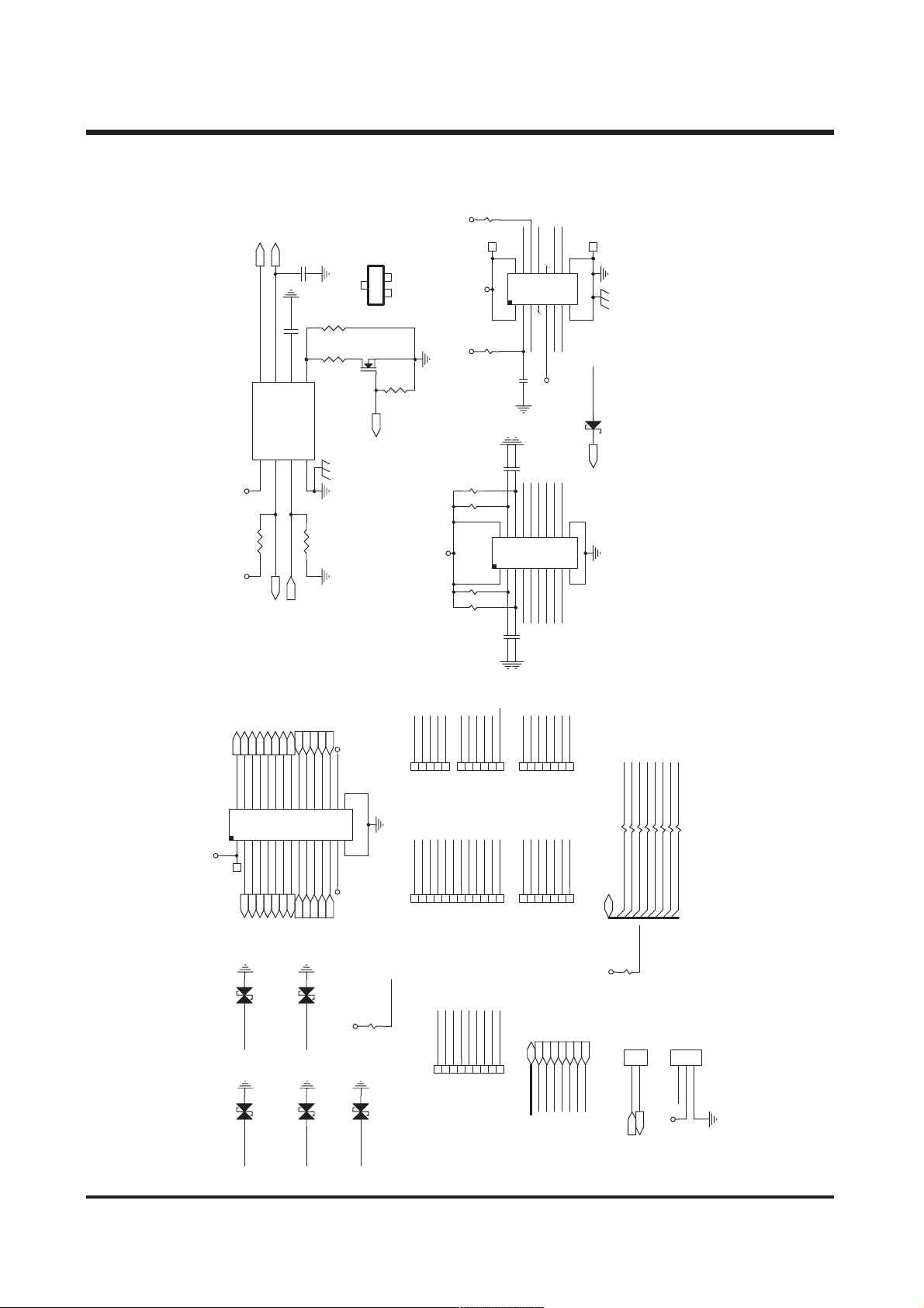
68
Ⅵ. CIRCUIT DIAGRAM
68686868
9) INTERFACE IO
CHARGE_O
CHARGE_FB
C201
100P
C0402
3
12
SOT-23-A
C0805
R262
90K9 1%
P
DUTYGND
TSSOP-8
R0402
R265 1M
TGGPIO8
0=DISABLE
1=ENABL E
R0402
R266
53K6 1%
R0402
Q15
MTN7002N3
32
1
DUTY
Frequency : 100KHz
DutyCycle :
BATT>2.8V=50%
3
SOT-2
R263
TGGPIO6
TGGPIO6
BATT<2.8V=70%
CHARGE_FB
CHARGE_O
C200 2.2u
2348
FB
SS
OUT
CHARGE
READY
VCC
U12 AT1453B
1
7
65
R0402
R264 100K
P3V3_SYS P3V3_SYS
TGGPIO23
0=NORMAL
1=READY
CHARGE
STROBE READY
R0402
100K
BATT>2.8V=1
BATT<2.8V=0
P3V3_SYS
P3V3_SYS
180
TP
BATT
P3V3_SYS
10K
10K
JP3
10K
10K
JP2
C192
NC
R176
R175
SW_COL3
R174
R173
SW_COL1
NC
C191
R177 10K
SW_COL2
43216
R172 10K
NC
C190
C194
NC
SW_COL4
43216
5
78
SD_D3 SW_COL0SD_D1
SW_COL2
NC
C193
SW_COL5SW_COL1
PWR_SW
5
78
9101113
P5V_SYS
SD_WP
SD_D2
SD_CD
121416
9101113
SD_D0
SD_CLK
SD_CMD
12
14
16
15
CHARGE_O TRIGGER
CHARGE_O CHARGE_FB
D17
READY_LED
AF_LEDSW_COL0
20
15
17 18
19
RESETb
TP183
CON-1010LM/16P
TRIGGER
12
SOD323
1SS355
RESETb
FPC-20P
KEY_CONN_
FLASH_CONN_
JP1
P3V3_SYS
USB_DET
SELFTIME_LED
ISP
SELFTIME_LED
USB_DET
ISP
43216
5
179
USB_LINK
VIDEO
TP
USB_LINK
VIDEO
12
D13
12
D12
SW_COL0 SW_COL2
DM
HP_R
HP_L
MIC-
HP_RHP_DET
HP_L
DM
MIC-
SP-
78
910
11 12
13 141715 16192123252729 30
DP
VIDEO_DET
MIC+
SP+
VIDEO_DETDPHP_DET
MIC+
SOD523
ESD 6.8S/NC
SOD523
ESD 6.8S/NC
SP-
IRIS_O1
IRIS_O1
AF_O2A
+
AF_O2A
SP
D15
D14
IRIS_O2
IRIS_O3
IRIS_O4
IRIS_O4
IRIS_O2
IRIS_O3
20
AF_O2B
AF_O1A
AF_O1B
AF_O1A
AF_O2B
AF_O1B
12
ESD 6.8S/NC
SW_COL3
12
ESD 6.8S/NC
SW_COL1
TOP5V_SYS
P4V_MO
AF-EAF-C
2826242218
AF-C AF-E
SOD523
SOD523
CON-1000LM/30P
P3V3_SYS
12
D16
ESD 6.8S/NC
SW_COL4
SW_COL2
SW_COL1
CHARGE
SW_COL4
SW_COL0USB_LINK
186TP185TP191TP189TP213
TP
VIDEO_DET
VIDEO
DP
194
TP
HP_DET
USB_DET
SW_COL3
PWR_SW
READY
TRIGGER
SW_COL5
207TP210TP203
TP
AUDIO
HP_L
HP_R
SELFTIME_LED
DM
READY_LED
2
219TP123
TP12
TP
AF_LED
USB / AUDIO/VIDEO
209
199TP202
TP
TP
TP206
RESETb
SD_CMD
SD_D0
SD_CLK
SD_D1
SD_D2
195TP192TP208TP211TP214
198
204TP201
TP
TP
TP
212
TP
SD_CD
215
TP
SD_WP
217
TP
VIDEO_DET
R178 47K
SOD523
187TP193TP196
184
TP
TP
190
TP
SD_D3
IRIS_O1
AF_O2B
AF_O2A
AF-C
5
0
TP4
TP39TP23
MIC-
SP+
MIC+
SP-
243TP231
2TP1
TP
TP
PWR_SW
SW_COL[0..5]
SW_COL[0..5]
READY
PWR_SW
IRIS_O3AF_O1A
IRIS_O2
1
TP4
AF_O1B
8TP43
5TP42
TP3
TP3
READY
CHARGE
TRIGGER
CHARGE
TRIGGER
1TP44
TP24
IRIS_O4 AF-E
READY_LED
AF_LED
SELFTIME_LED
READY_LED
AF_LED
SELFTIME_LED
SD_CLK
SD_D3
33R
33R
12
12
RP9-1
RP10-1
FMGPIO[42..0]
FMGPIO6
FMGPIO7
P3V3_SYS
1
RS232
GPIO17
0
TXD
SD_D2
SD_D0
SD_D1
33R
33R
34
78
56
RP10-3 33R
RP9-2
RP9-4
FMGPIO9
FMGPIO8
FMGPIO11
RXD0
R179 10K
CON1X2-SMD
J2
RS232
2
GPIO16
RXD0
SD_CMD
SD_WP
SD_CD
33R
33R
33R
56
34
78
RP9-3
RP10-2
RP10-4
FMGPIO12
FMGPIO41
FMGPIO42
1
RESETb
P3V3_SYS
CON1X3-SMD
J3
P/G/RS
3
2
Page 68
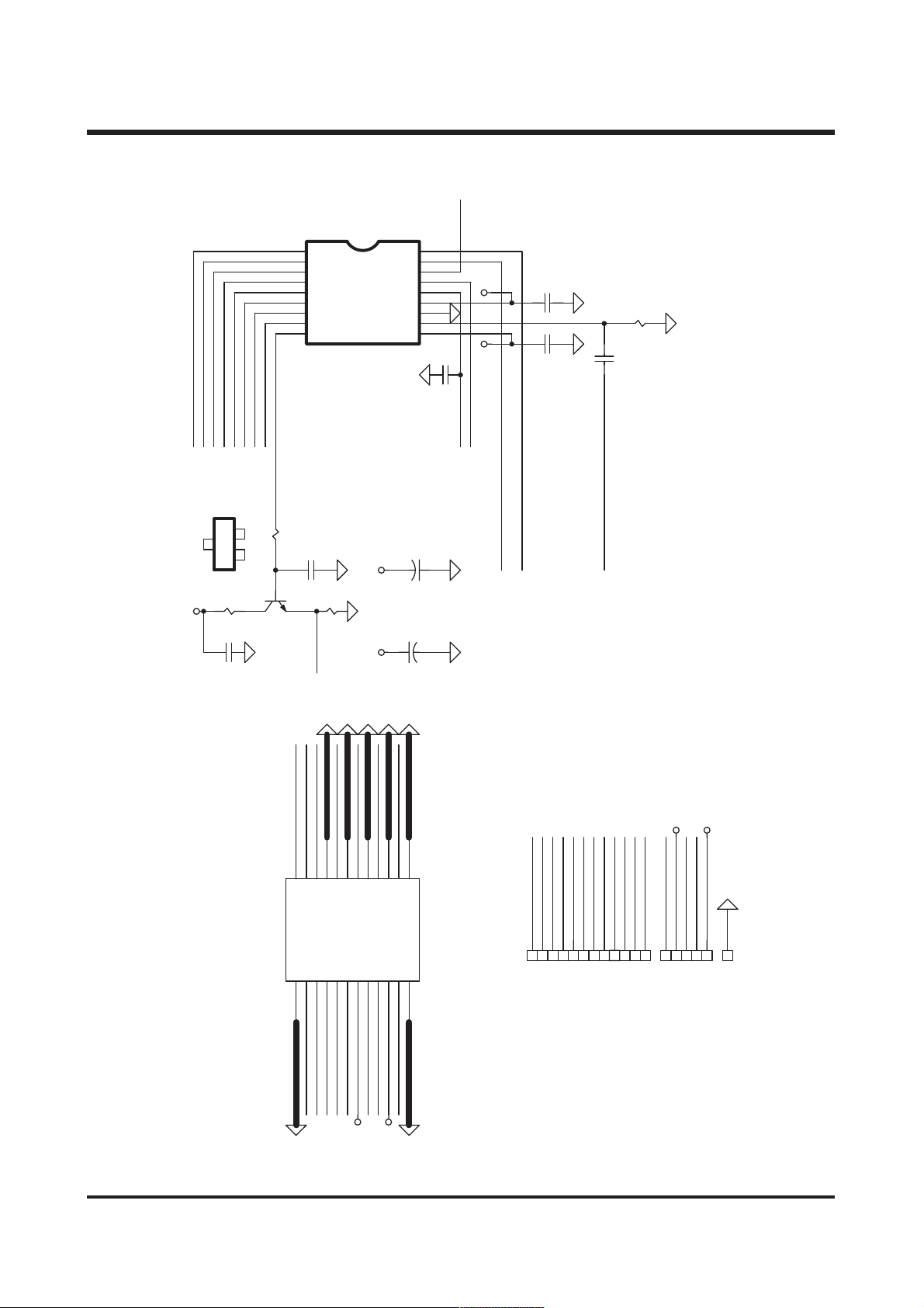
69
Ⅵ. CIRCUIT DIAGRAM
696969
10) IMAGE SENSOR FPC-MN39620
69
CCD_V6
CCD_V5B
CCD_V5A
3
R1
CCD-VH
CCD_V3B
CCD_V4
CCD_V3A
12
SOT-23-A
100R
C1
104P
C0402
V6
1
V5B
2
V5A
3
V4
4
V3B
5
V3A
6
V2
7
V1
8
VOVOD
910
CCD_V1
CCD_V2
47R
R2
3
Q1
2
2SC4083
C0402
C2
NC
R3
1K2
1
3
CCDIN
SOT323_UMT
H2
18
H1
17
HL
16
SUB
15
CSUB
14
VPT
13
PW
MN39620
U1
Panasonic 1/2.5"
CCD\DIP18\44
#13#10
CCD-VL
CCD-VH
RG
C3
+
12
11
C5
4.7u/16V
+C42u2/16V
C0805
4.7u/16V
2u2/16V
C0805
104P
CCD_HL
CCD-VL
CCD-VH
C0402
CCD_SUBCTRL
CCD_SUB
CCD_H1
C9
C8
CCD_H2
104P/NC
C0402
C0402
104P/NC
R4
103P
C0402
C12
CCD_RG
1M
CCD_V3A
2
CCD_V3A
GND
CONN1
1
CCD_V2
CCD_V1
8196
4
GND
CCD_V2
CCD_V1
CCD_V3B
CCD_V4
CCD_V5A
357
CCD_V5A
CCD_V4
CCD_V3B
CCDIN
CCD_HL
CCD_H2
102114131822
CCD_OUT
CCD_V5B
9
CCD_V5B
12
16
GND
CCD_HL-8V
CCD_V6
151723
11
CCD_V6
CCD_SUB
CCD-VL
GND
SUB
20
GND
CCD_H2
+12V
CSUB
CCD_SUBCTRL
CCD-VH
CCD_H1CCD_RG
24
GND
CCD_H1
CCD_RG
GND
FPC2X12_PTH0.4
CCDIN
CCD_V1
CCD_FFHL
TP3
TP2
TP1
CCD_V2
CCD_V3A
CCD_V3B
TP4
TP5
CCD_V5A
CCD_V4
TP6
TP7
CCD_V5B
CCD_V6
TP9
TP8
TP10
CCD_H1
CCD_H2
TP11
TP12
CCD-VH
CCD_SUBCTRL
CCD_SUB
CCD_RG
TP15
TP14
TP16
CCD-VL
TP17
TP18
TP19
Page 69
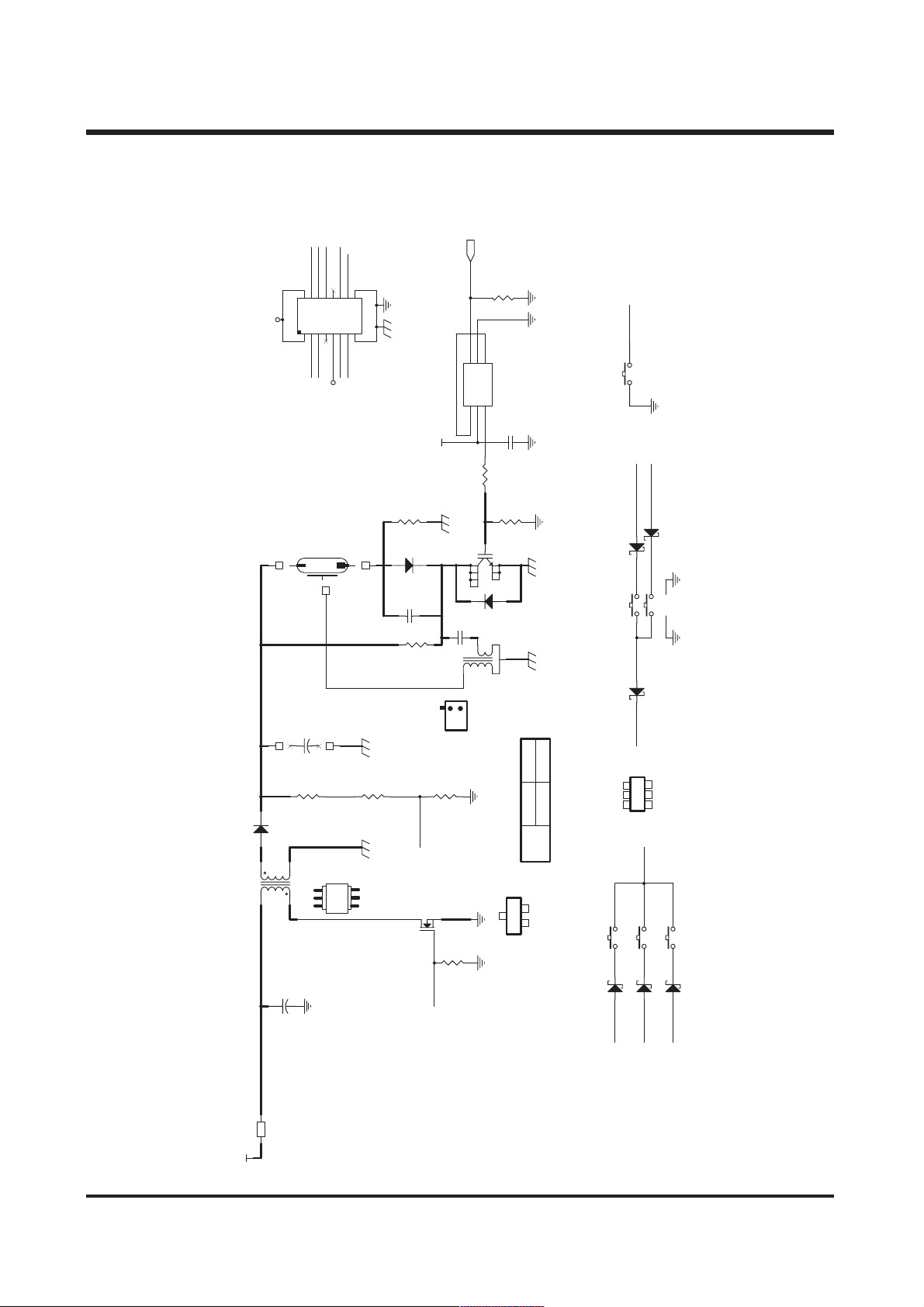
70
Ⅵ. CIRCUIT DIAGRAM
70707070
11) STROBE FLASH
TRIGGER
1=TRIGGER
0=NORMAL
TGGPIO47
SW_COL2
SW_COL5SW_COL1
PWR_SW
TRIGGER
CHARGE_FB
43216
12
14
T
BAT
JP1
SW_COL0
5
78
9101113
CHARGE_O
CHARGE_O
P5V_SYS
16
15
CON-1010LF/16P
FLASH_CONN_
500us
R10
100K
R0402
1
2
1A
2A
GND
1Y
VCC
2Y
U2
SN74LVC2G14
SOT-26_0.65
6543
C0402
C9
P5V_SYS
104P
R0603
PWR_SW
13
S1
PW- SW
SW4
T1
300V
12
ST-652277A
6 4
TP2
TUBE_P
TP1
CAP_P
D3
HMS17
PRI SEC
C2
35
TEST
35
TEST
D1FS4
3 1
220uF/6V
+
A
ST-652277
E
TANT-
STB1
C3
100uF/330V
+
R1
4M7 1%
R0603
STROBE TUBE
PAD-TUBE
TP3
TUBE_TRIG
35
TP4
CAP-N
TEST
123
456
TP5
35
TUBE-N
TEST
R2
4M7 1%
R0603
R4
100K
D4
F1SN4
12
C5
103P/500V
R5
32
R0603
D1FS4
C1210
1M
R0603
3
R6
1.1V
CHARGE_FB
3
Q1
AO3416
SOT-2
1
CHARGE_O
C8
1
33K 1%
R0603
R12
100K
203P/400V
T2
3
2
R0402
R9 0R
R11
4
IGBT 4.5~5V ON
SOP-8P
U3
1 5
6
2
7
3
8
12
D5
D1FS4
HMS17
C1210
1
TR0496
3
220R
R0603
2
TR-0466
SOT-23-A
4.5S
4V
BATT
12
11S
2V
IMN10
D2B
SHUTTER
IMN10
D2A
4
6 5
T
SW-SSQ-132MH
SW1-2
SW1-1
1 3
IMN10
6 1
D1A IMN10
D1B
SW_COL2
SW_COL1
43
IMN10
52
D2C
2 1
3 4
61
SW_COL0
SOT-26
123
T
SW_COL5
SW-SSQ-132MH
2 3
5 2
5 6
T
SW-SSQ-132MH
SW1-3
IMN10
D1C
4 3
4 3
SW_COL1
SW_COL0
SW_COL2
AVI
PLAYBACK
L1206
0R
BEAD
L1
T
BAT
CAPTURE
Page 70
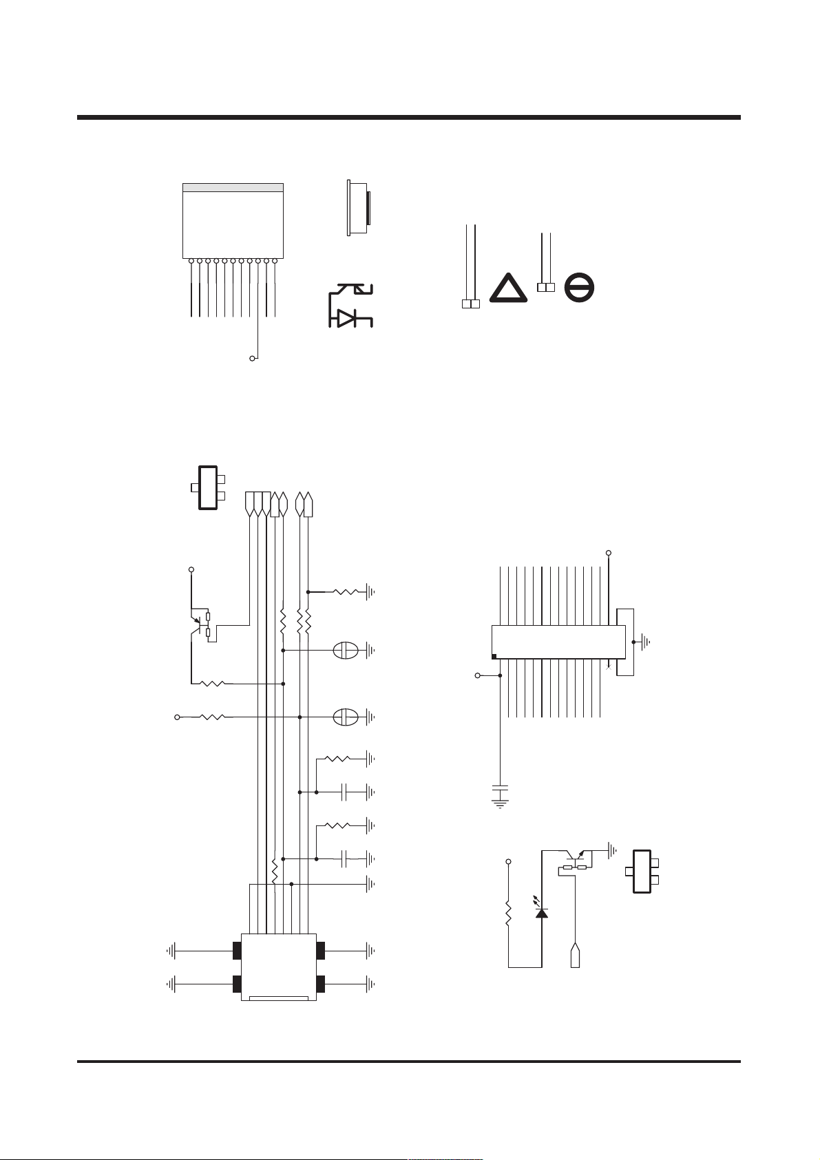
71
Ⅵ. CIRCUIT DIAGRAM
717171
12) USB/VO/AO/HEADPHONE/MIC/SPK
71
AFSM-B
AFSM-A(-)
VO1
VO2
VO3
AFSM-A
2
1
CONN1
FH19S-21S-0.5SH
FPC-11P
AF_O2A
AF_O1A
AFSM-B(-)
456
3
IRIS_O1
AF_O1B
AF_O2B
IRIS_O2
VO4
7
8
IRIS_O3
IRIS_O4
VDD
CATHODE
9
10
AF-E
AF-C
EMITTER
11
PIN1
down
SZB4325
R
EMITTE
PIN11
SP+
SP-
MIC-
MIC+
SP
MIC
SP1
SP2
1
MK2
MK
3
P3V3_SYS
13
10k
Q1
P3V3_SYS
12
SOT-23-A
SOT23
DTB113ZK
1k
R0402
R4
1K5
R3
R0402
NC/470K
P3V3_SYS
USB_LINK
VIDEO
TGGPIO13
2
USB_D+
ISP
VIDEO_DET
R0402
R6 27R
USB_D-
GPIO8
R0402
R0402
R8 47K
R7 27R
VDD
USB_DET
D2V4
R14
R11
C5
C4
47K
20P
20P
100K
R0402
C0402
C0402
R0402
CATHODE
USB_DET
USB_D-
HP_R
ISP
HP_L
SELFTIME_LED
MIC-
SP-
43216
USB / AUDIO/VIDEO
P3V3_SYS
JP1
5
78
VIDEO
USB_LINK
USB_D+
VIDEO_DET
910
11 12
13 141715 16192123252729 30
SP+
HP_DET
MIC+
IRIS_O2
IRIS_O1
IRIS_O3
20
18
AF_O2A
AF_O2B
AF_O1A
AF-E
IRIS_O4
22
AF_O1B
AF-C
TO
P4V_MO
282624
CON-1001LF/30P
R5 10K R0402
1658732
FOXCONN
G
9
910
Detect(Shell)
USB_A_GND
RCA_Video-O
RCA_Audio-O
USB_A_D+
USB_A_GND
GG
1011
USB1
UH51813-DHQ5
4
G
12
USB_A_D-
USB_A_VCC
11
C3
20P
C0402
R13
R0402
100K
C1
20P
C0402
12
USB-MINI-8P
USB 1.1
C0805
C12
TO
P4V_MO
100R
R12
10u/10V
R0402
3
Q2
DTC143XUA
4.7K
2
LED1
LED-2P/A
TGGPIO6
3
1
SOT323_UMT
SELFTIME_LED
SOT323_UMT3
SELFTIME_LED
10K
SOT-23-A
12
3
RED 5mm DIP
Page 71
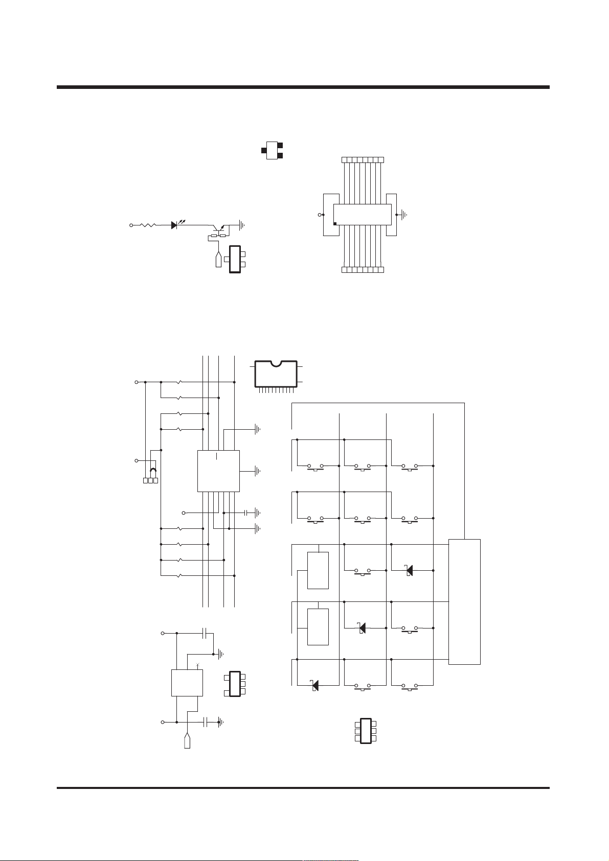
72
Ⅵ. CIRCUIT DIAGRAM
72727272
13) KEY/SD CON
R1
100R
R0402
P3V3_SYS
P3V3_SYSP3V3_SD
213
R3 P2 / P3
LAYOUTSHORT
KP-3015
LED1
GREEN
RP2-4
78
RP2-2
34
RP1-1
RP1-3
P3V3_SD
RP1-4
RP1-2
RP2-1
12
RP2-3
56
SD_D1
10K
10K
10K
1 2
10K
5 6
SD1
SD/MMC
1234567
10K
7 8
10K
34
10K
10K
3
Q1
4.7K
SD_D2
9811
DATA2
DATA1
CD/DAT3
CMD
GND
3
1
DTC143XUA
SOT323_UMT
10K
2
3
READY_LED
CARD DET
LO
CARD
SD_WP
SD_CD
10
12
CD
GND
VDD
CLK
GND
1
2
SOT-23-B
POTECT HI
14
WP
SD_ALPS_LCON
G
14
DATA
C4
22P
3
2 1
SOT323_UMT3
SW_COL3
AF RED
LED
P3V3_SYS
JP1
SW_COL1
POWER ON READY
GREEN LED
12
11
SDCON
912345678
13
C0402
10
SW_COL5
SW2
SW1
ZOUT
ZIN
SH2SH1
6TP8
4
2
TP
TP
TP
SD_D1
SW_COL4
43216
5
78
SW_COL2
SD_D3
0
SD_D2
SD_CD
SD_WP
121416
9101113
SD_D0
SD_CLK
SD_CMD
9TP3TP5TP1
TP
TP7
DEL
SW6
SW5
PLAY
LCD
SW4
TP15TP12TP1
TP14
READY_LED
AF_LED
20
15
17 18
19
RESETb
SW_COL0
3
1
TP1
TP1
TP16
FPC-20P
KEY_CONN_
SW10
RT
LF
SW9
D1C
IMN10
4 3
P3V3_SDP3V3_SYS
U1
AAT4250
1234
OUT
GND
IN
5
RESETb
SD_D3
SD_CMD
C3
104P
A
NCON
SOT-25_0.95
C2
10uF/10V
C0402
C0805
SD_CLK
45
SD_D0
SOT-26
D1B
IMN10
5 2
D1A
123
SW_COL0 SW_COL3SW_COL1 SW_COL2 SW_COL4
IMN10
6 1
SW3
OK
SW8
SW7
DOWN
UP
MODE-SW1
MODE-SW2 FL PCB
MODE-SW3
4
SOT-26
123
6 5
Page 72

ⅦⅦ.. TTRROOUUBBLLEESSHHOOOOTTIINNGG
73
11.. CChheecckk LLiisstt ffoorr rreeppaaiirriinngg
11)) WWhheenn rreecceeiivveedd
· Grasp customer's complaints exactely
· Check the product's condition of exterior view(damage by shock)
· Check the condition of battery and all kinds of cables(USB cable, AV cable, AC Adaptor)
· Check working condition with new battery or adaptor
- ON/OFF
- TELE/WIDE
- Check if the image shows correctly with TFT LCD on
(Turn on the TFT LCD and check if the image shows correctly)
- Take a picture by pressing the shutter button
- Turn the dial and check if modes change correctly
· Download from the camera by connecting it with PC and check if correctly
· Check if the image shows correctly with it connected to monitor
22)) WWhheenn rreeppaaiirriinngg
· Check the connectors' condition to each PCB(dirt, short, assembly, lean, etc.)
· Change each doubtful PCB one after another to find out bad PCB
- When doubtful of Main PCB Ass's, check the operating condition by assembling with a good
Main PCB ass'y (Manufacture of checking machine for each bad PCB is in schedule)
· Refer to each page to fix bad items of each PCB
· Check the connections of each PCB before assembling covers and embarkation of the parts
(soldering condition) with the naked eye
· Ateter assembling the camera, insert battery only when condition of the parts' embarkation
and connection is all right (Inserting battery when the camera has inside-short will result in death
or serious injury to the CPU and all parts)
· After setting the mode dial in position assemble the Top Cover and check if the dial nverts
correctly
33)) AAfftteerr rreeppaaiirriinngg
3-1) A/S Check list for each item
To judge inferior goods, begin with doubtful PCBs, replacing one after another to replace bad
parts
ex.) When Main PCB ass'y is in trouble, try replacing it with inferior camera's fair Main PCB ass'y
Page 73
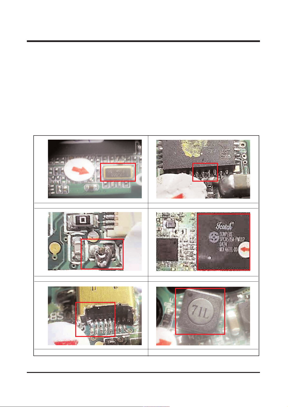
74
Ⅶ. TROUBLESHOOTING
MAIN Y2 has defect MAIN U9 causes a short circuit
MAIN L3 and C88 cause a short circuit U7 has defect
USB CON. causes a short circuit T1 has defect
22.. MMaaiinn TTrroouubblleesshhoooottiinngg
11)) PPoowweerr oonn ddeeffeecctt..
① Check the connection between each PCB(Check the connection of contactor)
- Check the soldering and battery leadwire condition Battery(87 PAGE)
- Check the connected condition between Main (CON3) and Shutter(CON1)(87 PAGE)
- Check the connected condition between Main (CON1) and Barrel(87 PAGE)
- Check the connected condition between Main (CON2) and CCD(87 PAGE)
② Check the below spare parts
Page 74
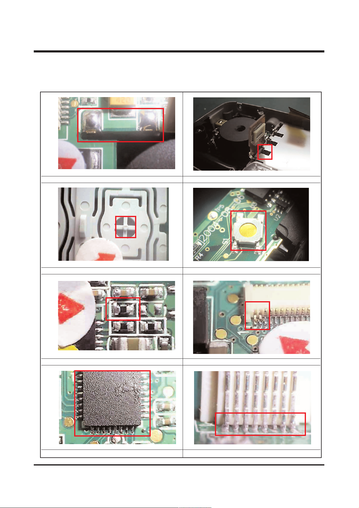
75
Ⅶ. TROUBLESHOOTING
BATTERY CON. has bad soldering BATTERY CON. is missing
POWER BUTTON has defect S1 switch has defect
R151 has bad soldering MAIN CON2 causes circuit-short
MAIN U1 has defect FLASH+MAIN connection has defect
Page 75
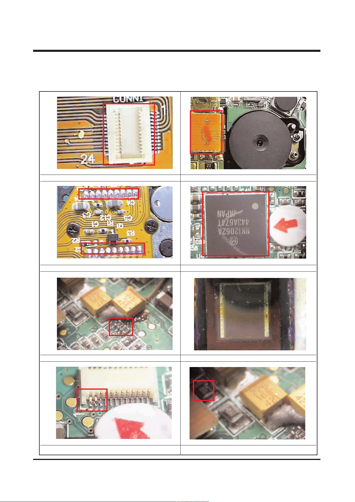
76
Ⅶ. TROUBLESHOOTING
CCD F PCB pattern causes circuit-short Assembly with CCD F PCB CON 1has defect
CCD soldering has defect Main U4 has defect
Main RP8 causes circuit-short Dirty on CCD
MAIN CON1 causes circuit-short MAIN L3 has defect
22)) DDeeffeecctt rreellaatteedd ttoo tthhee CCCCDD
① Check the connected condition with the Main (CON2).
Page 76
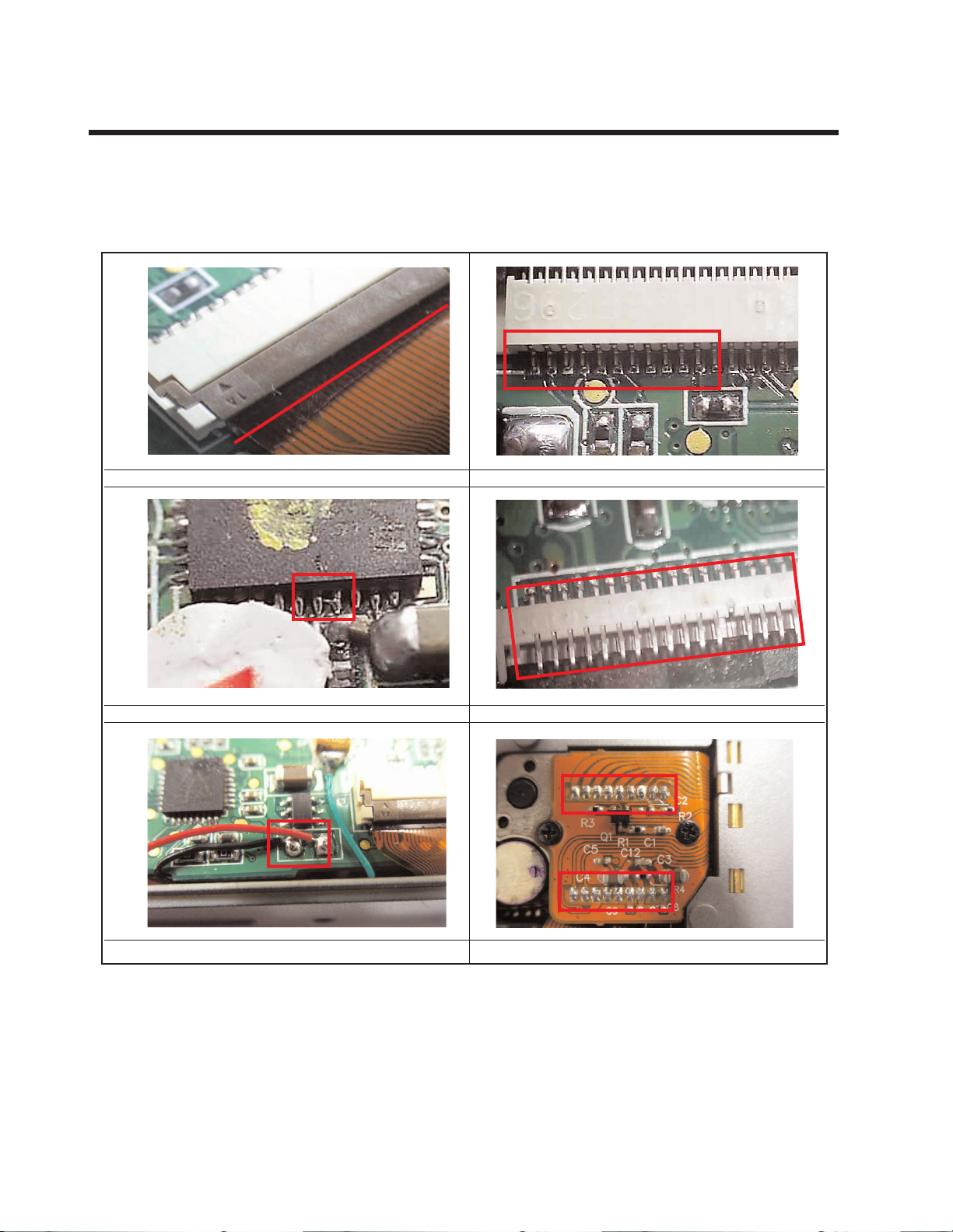
Ⅶ. TROUBLESHOOTING
Check the LCD F PCB connection MAIN TFT1 has bad soldering
MAIN U9 caused circuit-short Main CON2 comes out
Check the BACK LIGHT lead wire Check the assembly of CCD
33)) DDeeffeecctt rreellaatteedd ttoo tthhee TTFFTT LLCCDD
① Check the connected condition between Main (TFT1) and LCD.
IIff tthhee iimmaaggee iiss nnoott sshhoowwnn aass nnoorrmmaall oonn TTFFTT LLCCDD,,
Connect the camera using A/V CABLE with TV and check the image.
If the image on TV screen is normal, TFT LCD has problem and if not, CCD has problem.
Page 77
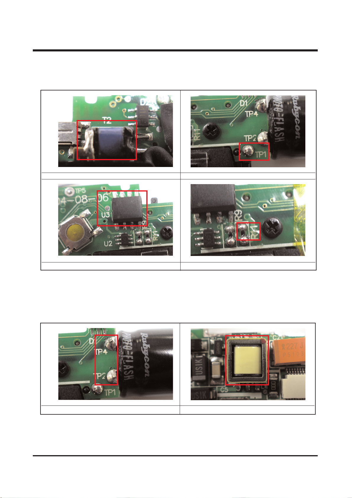
78
Ⅶ. TROUBLESHOOTING
44)) TThhee ddeeffeecctt ooff FFLLAASSHH rraaddiiaattiioonn
T2 has bad soldering Check the connection of TP1 (XE TUBE +)
U3 has defect R11 causes circuit-short
Check the charging voltage of MAIN CON. T1 has bad soldering
55)) TThhee ddeeffeecctt ooff FFLLAASSHH cchhaarrggiinngg
Page 78
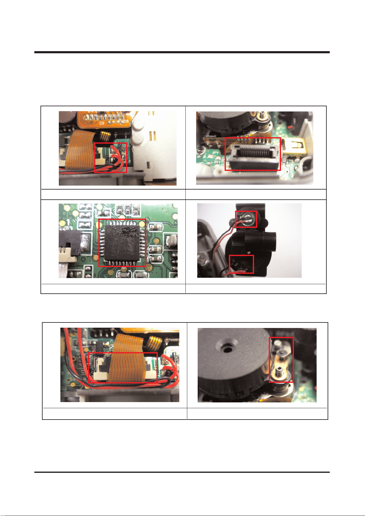
79
Ⅶ. TROUBLESHOOTING
Check the connection of lead wire with SPK. MIC Check the connected condition of MAIN+JACK
MAIN U1 has defect The lead wire of SPK. or MIC come out
66)) DDeeffeecctt rreellaatteedd ttoo tthhee AAUUDDIIOO
-- CChheecckk tthhaatt tthhee AAUUDDIIOO iiss oonn iinn tthhee MMEENNUU
-- BBee ccaarreeffuull ooff hhiigghh tteemmppeerraattuurree wwhhiicchh iiss ccaauusseedd ddeeffeecctt wwhhiillee tthhee MMIICC && SSPPEEAAKKEERR iiss ssoollddeerreedd
77)) DDeeffeecctt ooff AAFF
The connection of F PCB has defect. AF MOTOR is stuck
Page 79
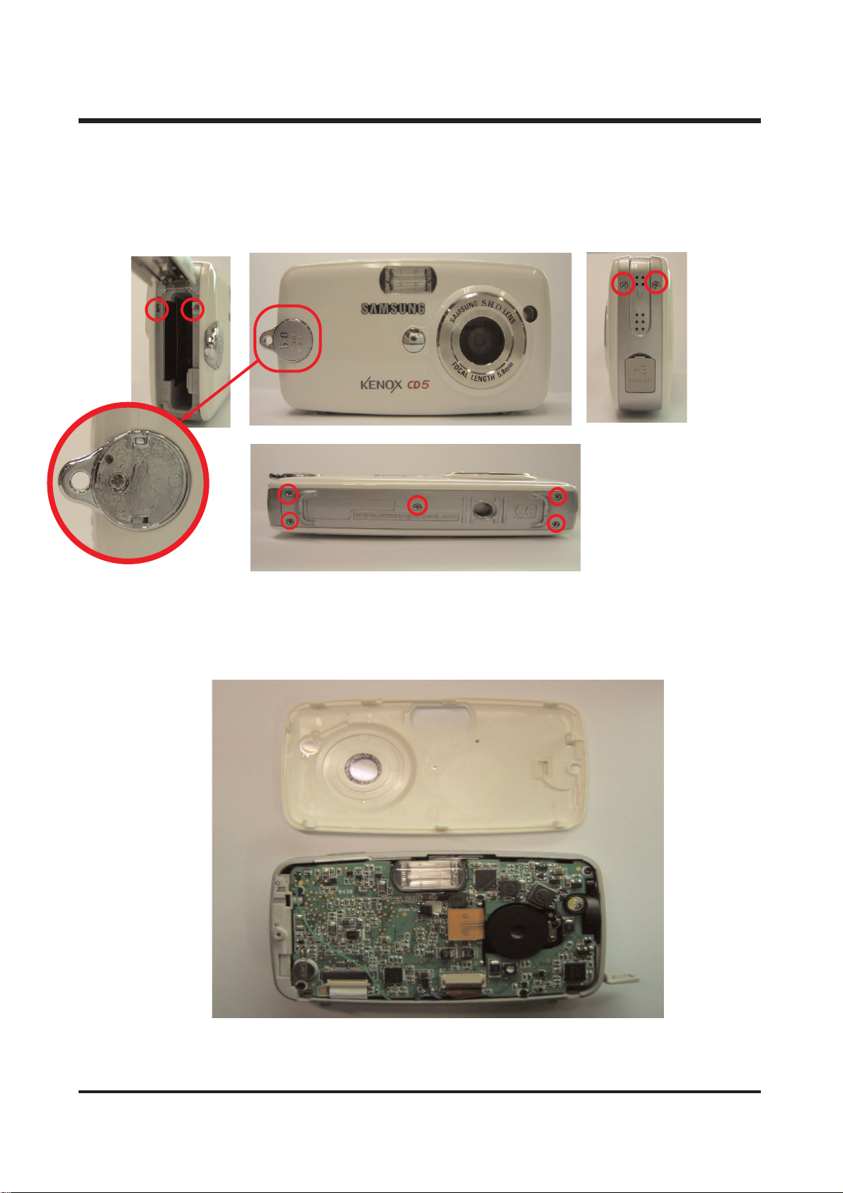
80
Ⅶ. TROUBLESHOOTING
8080
2. Take off the FRONT COVER.
1. Remove the 9 SCREWS at the outside of camera and 1 screw under the Strap ring decoration..
33.. HHOOWW TTOO DDIISSAASSSSEEMMBBLLYY
Page 80
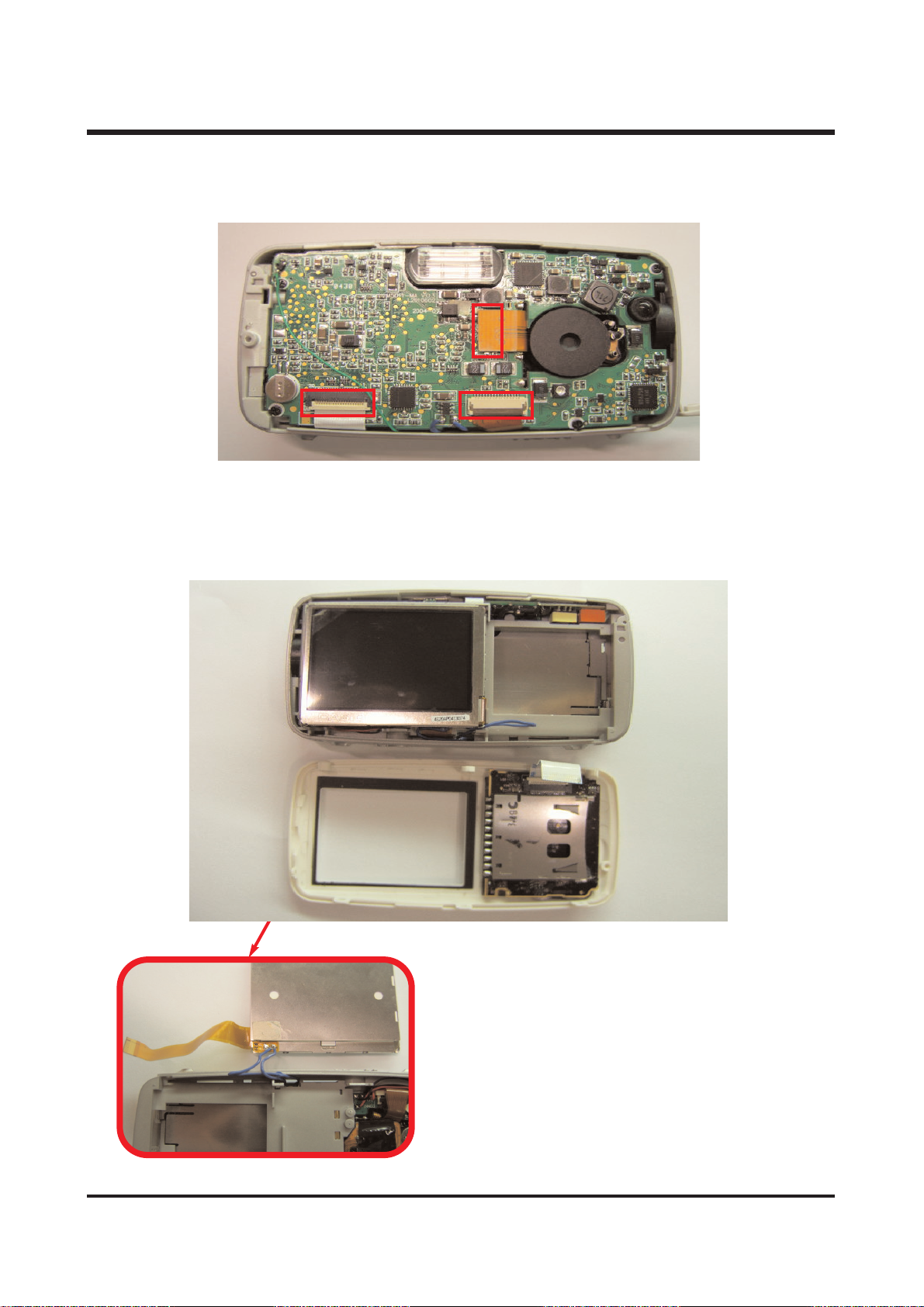
81
Ⅶ. TROUBLESHOOTING
8181
4. Disassemble the BACK COVER. Remove the Lead wire that is connected with LCD.
3. Remove the connector that is connected with the MAIN BOARD.
Page 81
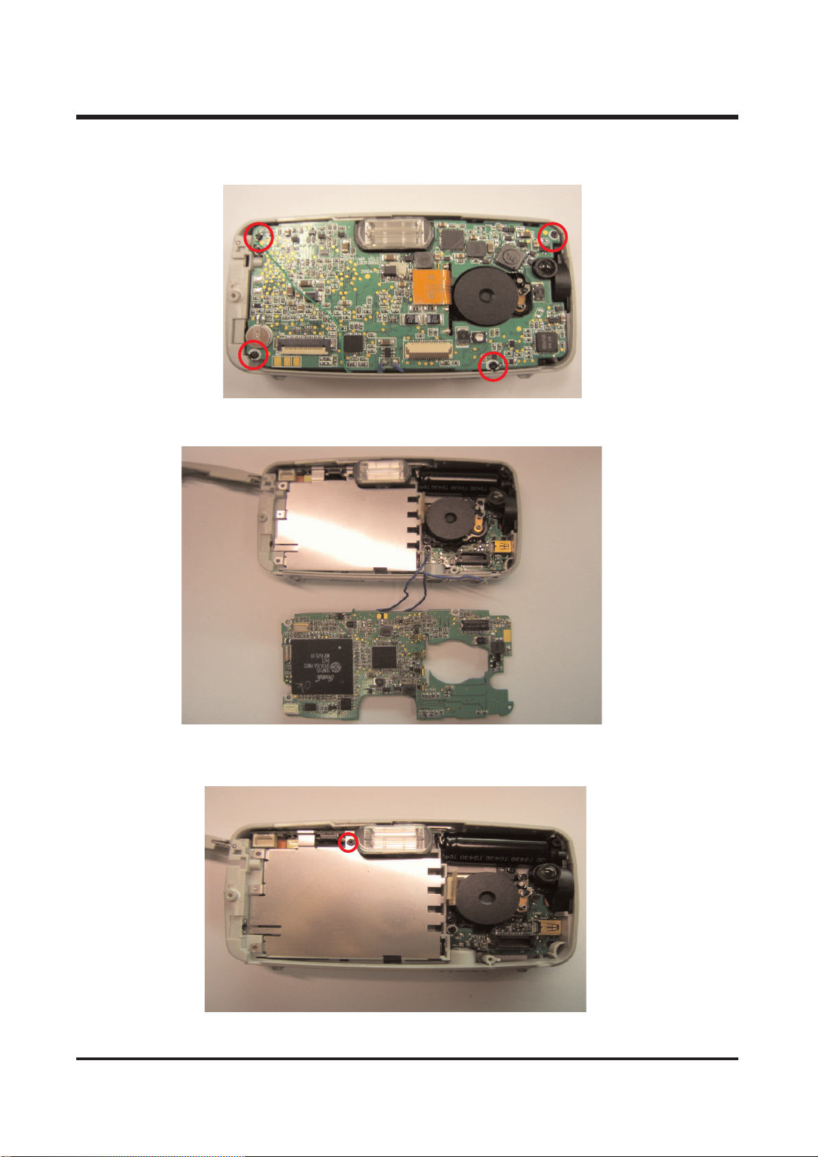
82
Ⅶ. TROUBLESHOOTING
8282
5. Remove 4 screws to take off the MAIN BOARD.
6. After remove the MAIN BOARD.
7. Remove the 1 screw to take off the Battery Holder Sheet.
Page 82
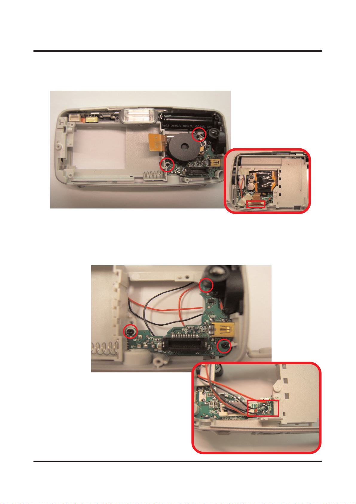
83
Ⅶ. TROUBLESHOOTING
8383
8. Remove the TOP BOARD and remove 2 screw to take off the LENS MODULE. Remove the connector in
the other side. which is connected with USB Board.
9. To remove the USB BOARD, remove the 3 screws and lead wires that are connected with Speaker and Mic.
Page 83
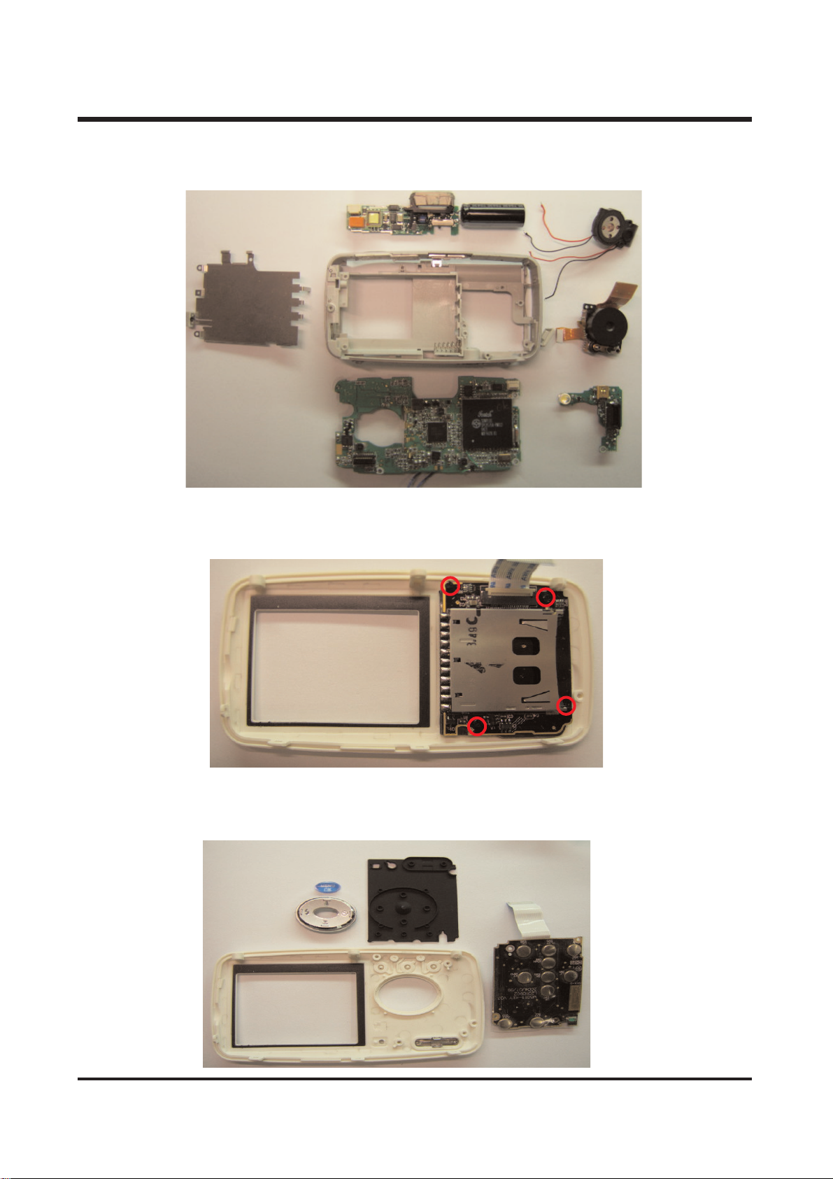
84
Ⅶ. TROUBLESHOOTING
8484
12. Disassembly of BACK COVER is completed.
11. To disassemble the BACK COVER, remove 4 screws.
10. Disassembly of BODY is completed.
 Loading...