

Samsung SM-G850 Troubleshooting
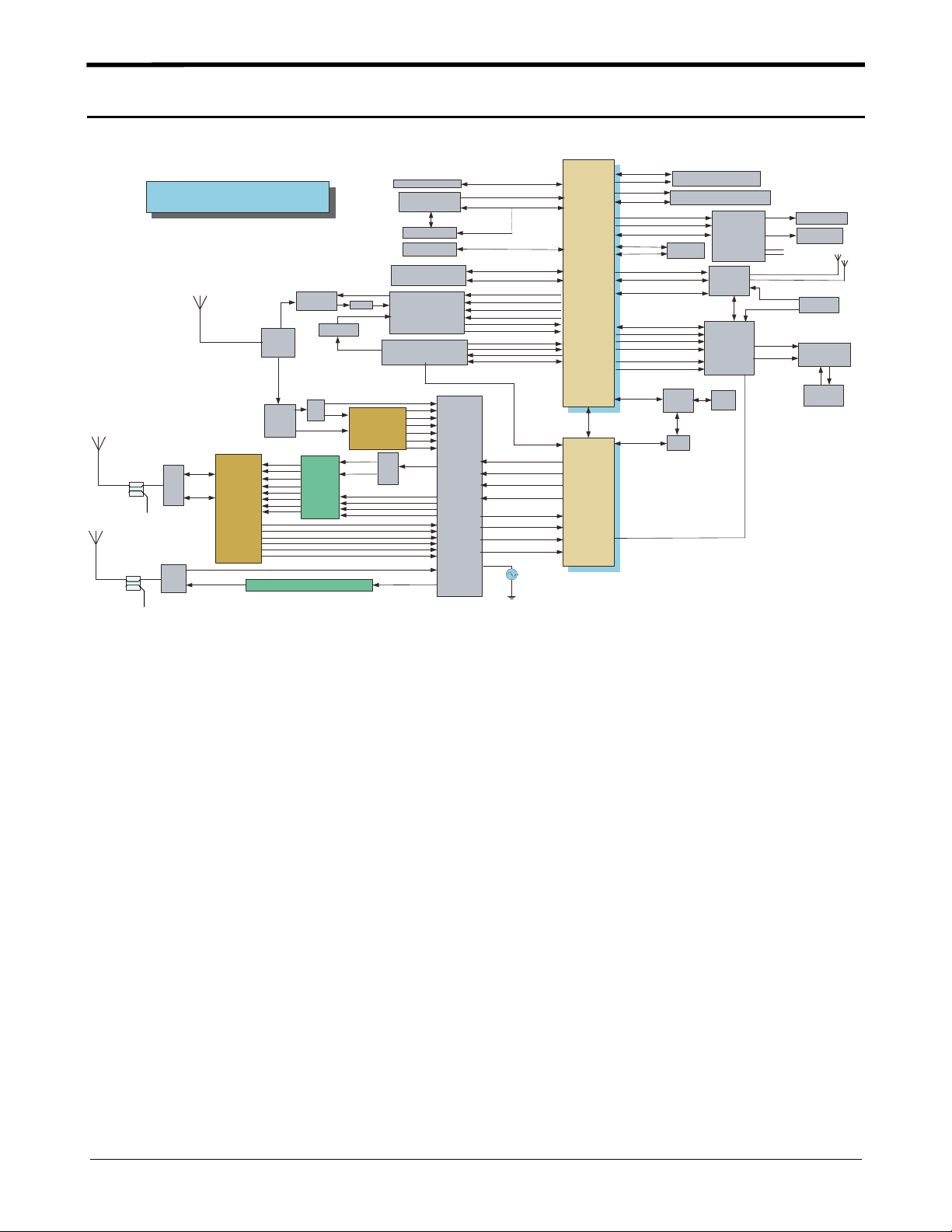
Level
8.
Block Diagram
8-1.
Repair
3
MAINANT(RX/TX)
G850,G900
DCS1800,PCS1900
WCDMA 1/2/5/8
MAIN ANT(RX/TX)
G850,G900
DCS1800,PCS1900
WCDMA 1/2/5/8
FBR_REV_HB
FBR_MAIN
SM-G850F Block Diagram
GGPPSS AANNTT
SUBRX
G850,G900
DCS1800,PCS1900
WCDMA 1/2/5/8
DIPL
EXER
DUPLE
XER
LTE B 1/B2/B3/B5/B8/B20
HHIIGGHH
LLOOWW
LMSWY4GR-
RF PATH
SWITCH
(MAIN
FEMID)
G78
Extract or
B8636
DIPLEXER
2G_HB_PA_OUT
2G_LB_PA_OUT
TX_B1_PA_OUT
TX_B2_PA_OUT
TX_B3_PA_OUT
TX_B5_PA_OUT
TX_B8_PA_OUT
TX_B20_PA_OUT
BAND7 PAM SKY77778-51
SUB_ANT
GGPPSS LLNNAA
BGS824N6S
RF
SW
MMMB PA
RF8095
B7_RX
PMIC_32K
MB_DRX
LB_DRX
GGPPSS__LLNNAA__EENN
SAW
GGPPSS_ _RRFF
GGPPSS__CCLLKK3322KK
RRTTCC OOUUTTPPUUTT
DIV_B7_RX
(SUB_ MLB _FEMID)
HFQSWBYUA-253
RRFFEE__VVCCCC__EETT
RRFFEE__VVCCMMOOSS__MMMMPPAA
B1 RX
B2 RX
B3 RX
B5 RX
B8 RX
B20 RX
GGPPSS__RRFF
RF PATH
SWITCH
2G3G_HB_TX
2G3G_LB_TX
PAM
DCDC
RF80
81A
LTE_MB_TX
LTE_LB_TX
SSVVCC LLEEDD((RRGGBB))
CCoommppaanniioonn IICC
S5C73C1A01-L030
MMIIPPII
12M CAM
2M VT CAM
DDiissppllaayy
HD
GGPPSS
(BBCCMM4477553311AA11IIUUBB22GG))
PPMMIICC
S2MPS13X01- 6030
DIV B1 RX
DIV B2 RX
DIV B3 RX
DIV B5 RX
DIV B8 RX
DIV B20 RX
RRFFEE__PPAADDAACCCCFF
__110000DD__PP//NN
TTRRAANNSSCCEEIIVV
PMB5747
HB7_TX
SS__LLEEDD__II22CC__SSDDAA//SSCCLL
MMIIPPII
CCOOMMPP__FFRROOMM__SSPPII__SSCCLLKK//MMOOSSII//MMIISSOO//SSSSNN
VVTT__CCAAMM__SSDDAA//SSCCLL
MMIIPPII DDSSIIOO
TS_I2C _SDA/ SCL
GGPPSS__EENN
GGPPSS__IINNTT
GGPPSS__UUAARRTT__TTXXDD
GGPPSS__UUAARRTT__RRTTSS
GGPPSS__UUAARRTT__RRXXDD
GGPPSS__UUAARRTT__CCTTSS
AAPP__PPMMIICC__IIRRQQ
AAPP__NN__RRSSTT__IINN
AAPP_ _PPSS__HHOOLLDD
AAPP_ _PPMMIICC__SSCCLL//SSDDAA
3322KKHHZZ__CCPP
RFE_MPHY_SYS_CLK_EN
RFE_MPHY2_SYS_CLK_EN
RFE_MPHY_TX_DAT/DATX
RFE_MPHY 2_TX_DA T/D ATX
EERR
RFE_MPHY_RX1_DAT/ DATX
RFE_MPHY_RX2_DAT/ DATX
RFE_MPHY2_RX1_DAT/DATX
RFE_MPHY2_RX2_DAT/DATX
OCS
26MHz
AApppp..
PPrroocceessssoorr
EExxyynnooss55443300
HSIC
CCaallll
PPrroocceessssoorr
PMB9930
BBTTPP__SSPPII__MMIISSOO//MMOOSSII
BBTTPP__SSPPII__CCLLKK
SSEENNSSOORR__II22CC__SSCCLL
SSEENNSSOORR__II22CC__SSDDAA
IF_PMIC/SCL/ SDA
HRM_INT
NFC_I2C_SDA/SCL
WWLLAANN__SSDDIIOO__CCLLKK//CCMMDD
WWLLAANN__SSDDIIOO__DD[[00::33]]
MMMM__II22SS__DDII//DDOO
MMMM__II22SS__CCLLKK//SSYYNNCC
CCOODDEECC__RREESSEETT__NN
CCOODDEECC__L LDDOO__EENN
CCOODDEECC__IIRRQQ__NN
CCOODDEECC__SSSSPPII__SSCCKK//SSSSNN
CCOODDEECC__SSPPII__MMOOSSII/
XXTTAALL__2244MMHHzz__AAPP
NFC_I2C_SDA/SCL
SIM_CLK/IO /RST
USB
UART
BBTT_ _EENN//WWAAKKEE
BBTT_ _UUAARRTT
SSEENNSSOORR
/MMIISSOO
NNFFCC
S3FWRN5
SSIIMM
CCAARRDD
FFiinnggeerrpprriinntt SSeennssoorr
SSEENNSSOORR((6 AXIS MAGNETIC)
IIFF PPMMIICC
MAX77804KEWJ+7
MUIC
Switching Charger
Fuel Gauge
HHRRMM
Motor Driver
BT/WIFI
(SWB-B80)
BBTT__PPCCMM__CCLLKK//SSYYNNCC
BBTT_ _PPCCMM__IINN//OOUUTT__CCPP
AAuuddiioo CCooddeecc
WM5110ECS/ R
NFC
ANT
NNFFCC__SSWWPP
SSPPEEEECCHH__PPCCMM__CCLLKK//SSYYNNCC
SSPPEEEECCHH__PPCCMM__IINN//OOUUTT__CCPP
DDPP//DDMM
CCAAMMEERRAA FFLLAASSHH
BBTT__WWIIFFII__CCLLKK 3322KK
CCOODDEECC__CCLLKK 3322KK
HHPPOOUUTT__LL//RR
SSPPKK__PPDDMM__CCLLKK//
DDAATTAA
(MAX98504EWV+)
FFBB__SSPPKK__OOUUTT__PP//NN
HHaappttiicc MMoottoorr
SSUUBB FFPPCCBB
IIFF CCOONNNN
BBTT//WWIIFFII
AANNTT__MMAAIINN
BBTT//WWI IFFII
AANNTT__DDIIVVE ERRSSIITTYY
PMIC_32K
VVII--AAMMPP
SPEAKER
SPK_OUT_P/N
8-1
Confidential and proprietary-the contents in this service guide subject to change without prior notice.
Distribution, transmission, or infringement of any content or data from this document without Samsung’swritten authorization is strictly prohibited.
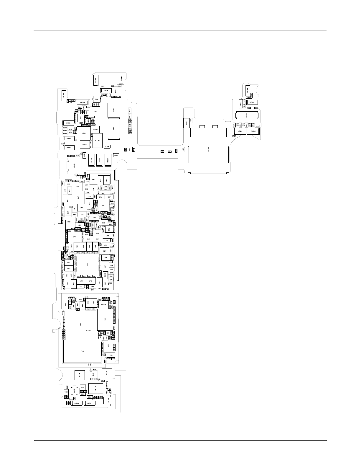
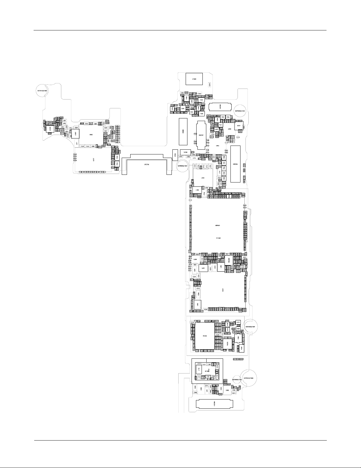
PCB Diagrams
8-2.
8-2-1.
Main PCB Top
Level3Repair
8-2
Confidential and proprietary-the contents in this service guide subject to change without prior notice.
Distribution, transmission, or infringement of any content or data from this document without Samsung’swritten authorization is strictly prohibited.
Level3Repair
8-2-2.
Bottom
8-3
Confidential and proprietary-the contents in this service guide subject to change without prior notice.
Distribution, transmission, or infringement of any content or data from this document without Samsung’swritten authorization is strictly prohibited.
Level3Repair
8-2-3.
Sub PCB Top
8-4
Confidential and proprietary-the contents in this service guide subject to change without prior notice.
Distribution, transmission, or infringement of any content or data from this document without Samsung’swritten authorization is strictly prohibited.
Level3Repair
8-2-4.
Sub PCB Bottom
8-5
Confidential and proprietary-the contents in this service guide subject to change without prior notice.
Distribution, transmission, or infringement of any content or data from this document without Samsung’swritten authorization is strictly prohibited.

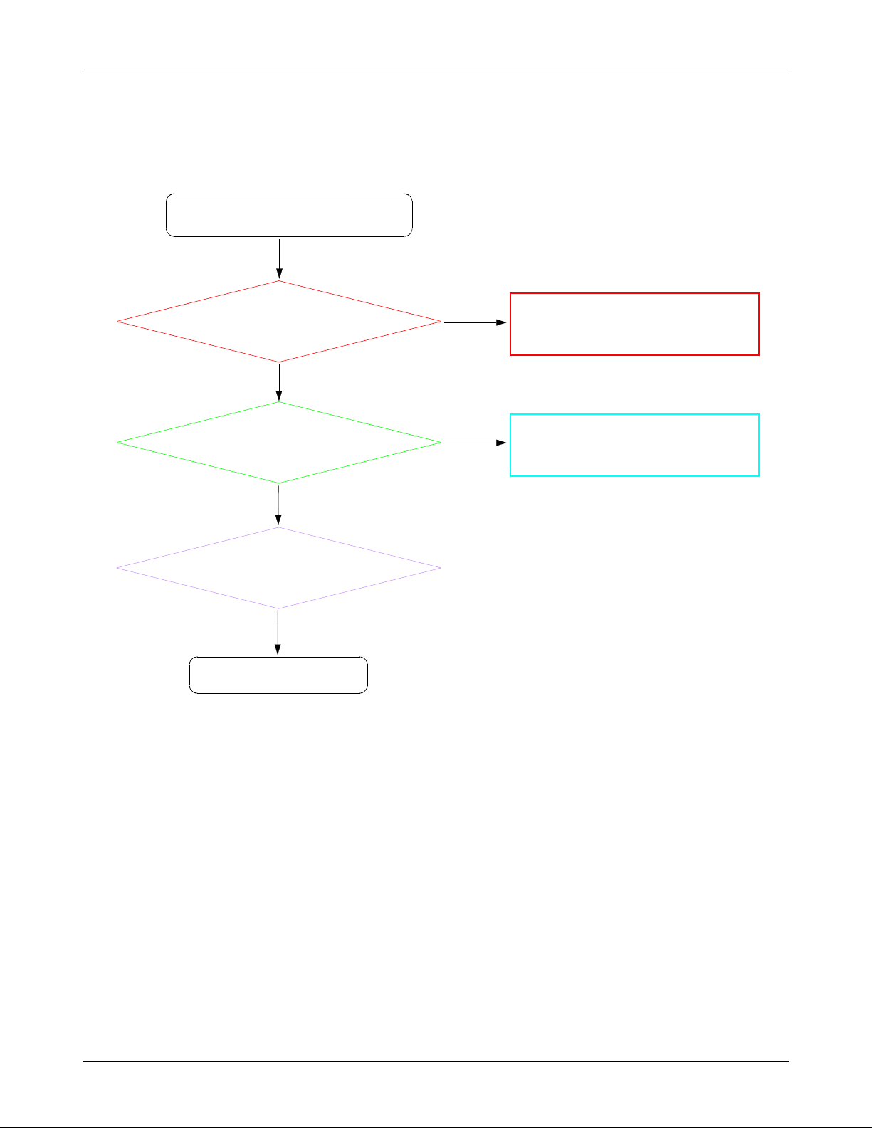
Flow Chart of Troubleshooting
8-3.
Equipments
Level3Repair
Oscilloscope
Power Supply
á
Digital Multimeter
á
driver, ESD Safe Tweezer
á+
8960 &
Confidential and proprietary-the contents in this service guide subject to change without prior notice.
Distribution, transmission, or infringement of any content or data from this document without Samsung’swritten authorization is strictly prohibited.
Spectrum Analyzer
8-6
Soldering iron
á
Level3Repair
8-3-1.
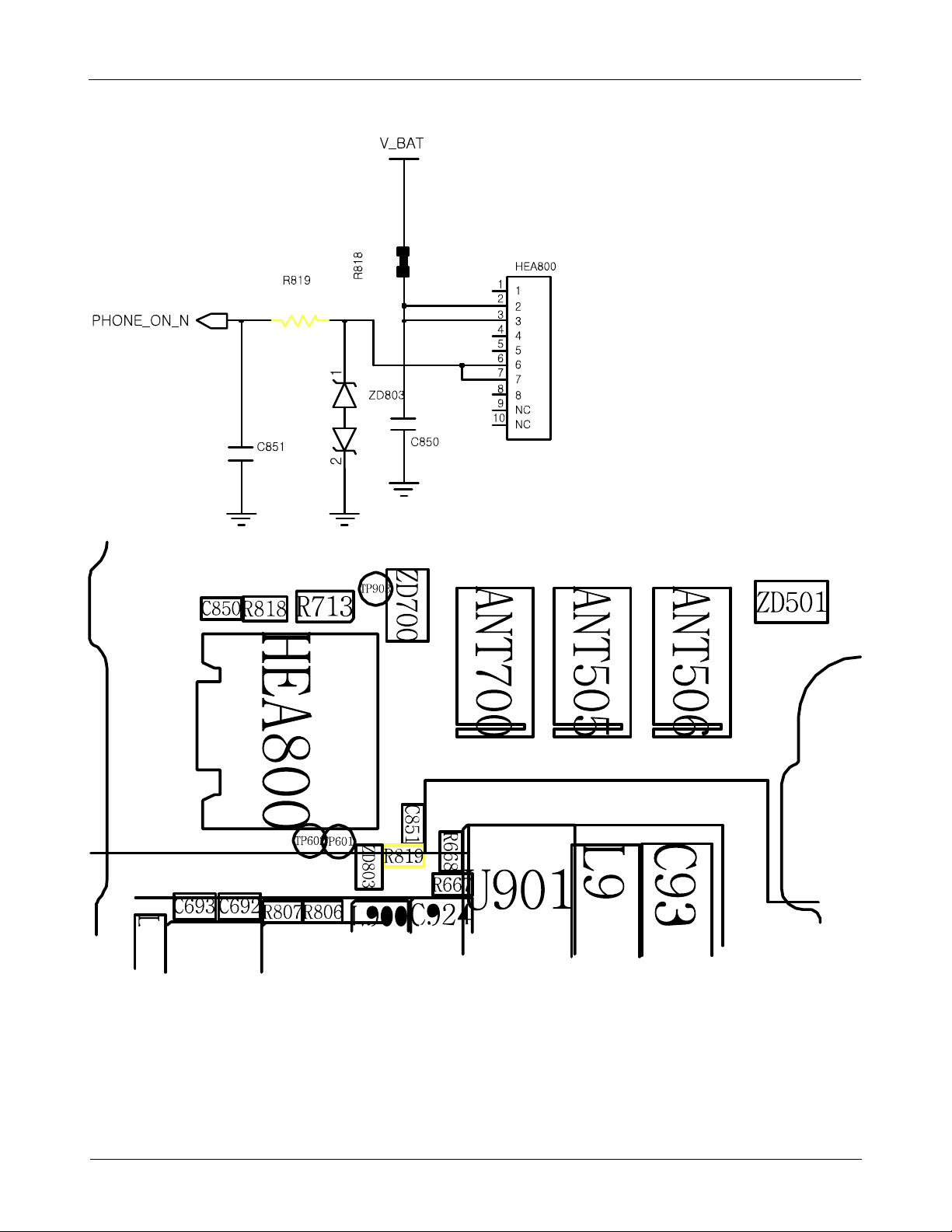
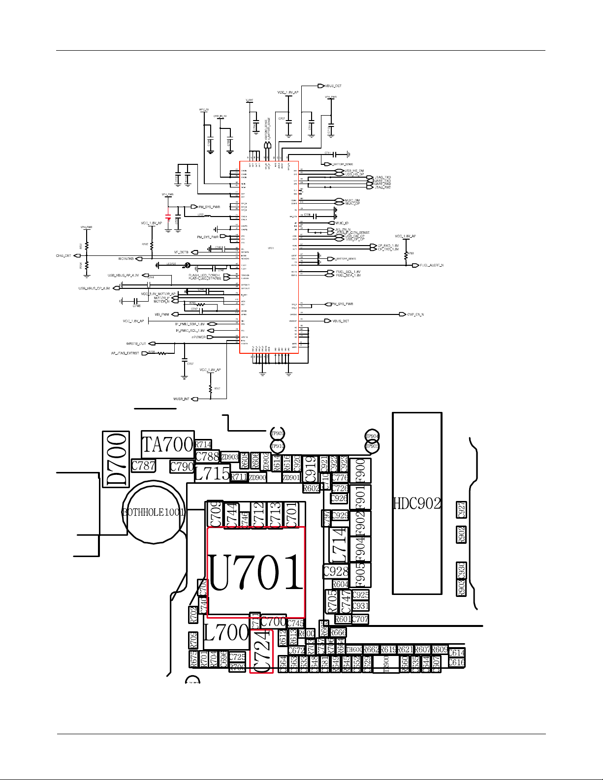
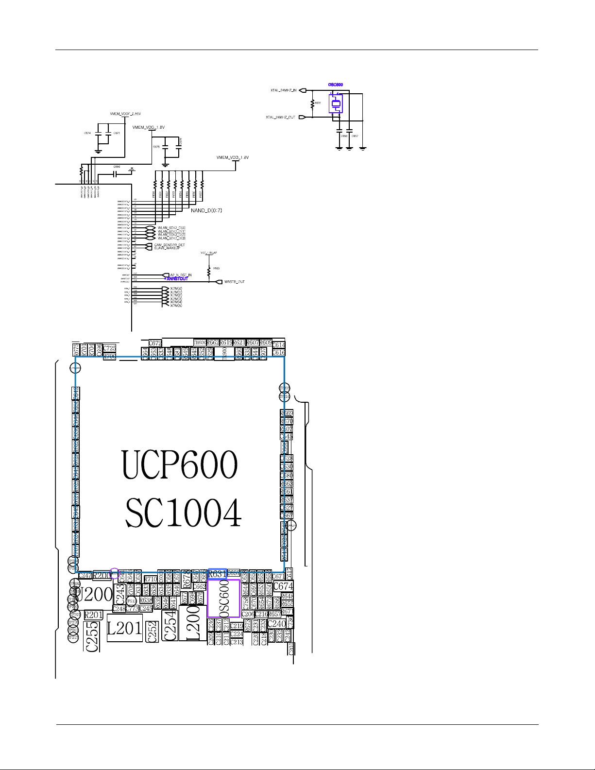
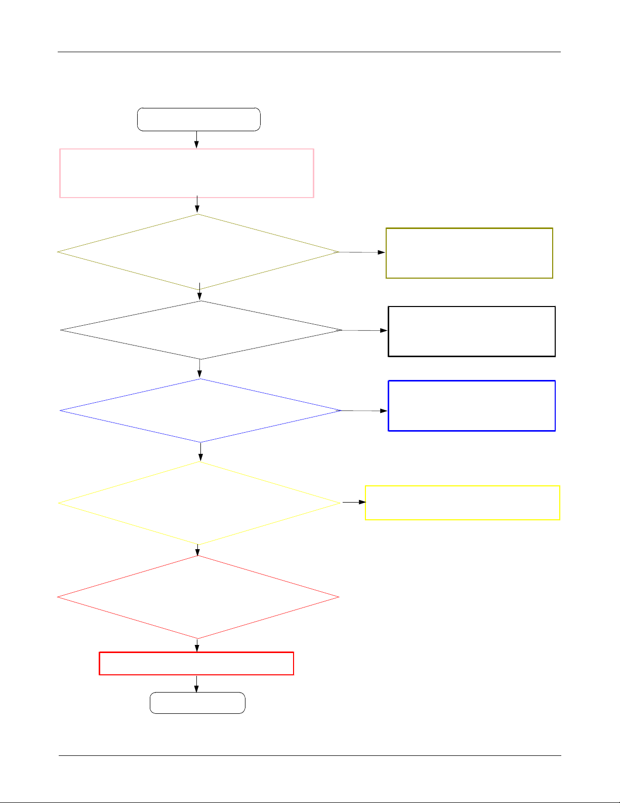
Power On
Cell-phone can`t power on.
Check the Battery Voltage
Battery
Power-on the phone and check
the power-on sound
or motor vibration.
If power key is pressed, is the
voltage of R819 High
Check the Vbatt(+point) of
4.4V)?
IF PMIC output
C724
(
=3.5~4.4
>3.4
Yes
No
Yes
V?
(3.5 ~
.
V)
No
No
No
Yes
If the output voltage is not satisfied with normal
condition, replace U701
Connect TA to charge the battery.
Change the LCD ASSY
Change the Power-key FPCB.
And retry to the power-on operation.
.
Yes
Check the voltage of
XNRSTOUT TP
XNRSTOUT=1.8V)
(
Yes
Check the frequency of main
clock OSC500(R631=24MHz)
Yes
check the initial operation
Yes
END
No
No
If the output voltage is not satisfied with normal.
condition, replace U702
Change the OSC600
If OSC600 still does not work, replace UCP600
Test condition(Oscilloscope setting)
※
us.div(time division)
:1.0
8-7
Confidential and proprietary-the contents in this service guide subject to change without prior notice.
Distribution, transmission, or infringement of any content or data from this document without Samsung’swritten authorization is strictly prohibited.
Level3Repair
8-8
Confidential and proprietary-the contents in this service guide subject to change without prior notice.
Distribution, transmission, or infringement of any content or data from this document without Samsung’swritten authorization is strictly prohibited.
Level3Repair
8-9
Confidential and proprietary-the contents in this service guide subject to change without prior notice.
Distribution, transmission, or infringement of any content or data from this document without Samsung’swritten authorization is strictly prohibited.
Level3Repair
8-10
Confidential and proprietary-the contents in this service guide subject to change without prior notice.
Distribution, transmission, or infringement of any content or data from this document without Samsung’swritten authorization is strictly prohibited.
Level3Repair
8-11
Confidential and proprietary-the contents in this service guide subject to change without prior notice.
Distribution, transmission, or infringement of any content or data from this document without Samsung’swritten authorization is strictly prohibited.
Level3Repair
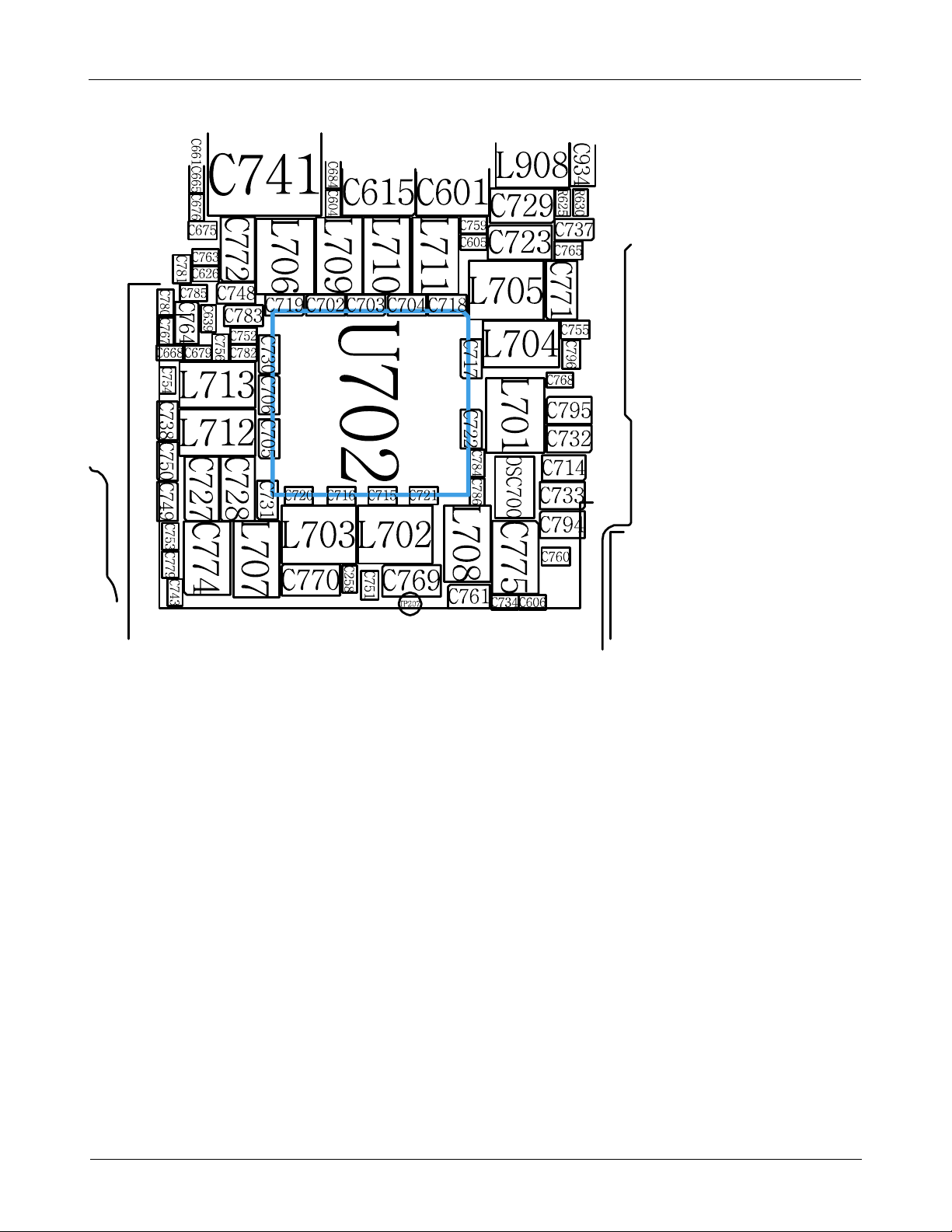
8-3-2.
Initial
Initial Failure
Yes
Re-download Software
Abnormal
Check the AP_PS_HOLD
TP701
(
Check the
C694=2.9V, C693=1.8V)
(
V)
=1.8
No
eMMC Supply
Normal
Yes
Check other part failure
No
Change the U600
Change UCP600
Abnormal
Change PBA
END
8-12
Confidential and proprietary-the contents in this service guide subject to change without prior notice.
Distribution, transmission, or infringement of any content or data from this document without Samsung’swritten authorization is strictly prohibited.

Level3Repair
8-13
Confidential and proprietary-the contents in this service guide subject to change without prior notice.
Distribution, transmission, or infringement of any content or data from this document without Samsung’swritten authorization is strictly prohibited.
Level3Repair
8-14
Confidential and proprietary-the contents in this service guide subject to change without prior notice.
Distribution, transmission, or infringement of any content or data from this document without Samsung’swritten authorization is strictly prohibited.
Level3Repair
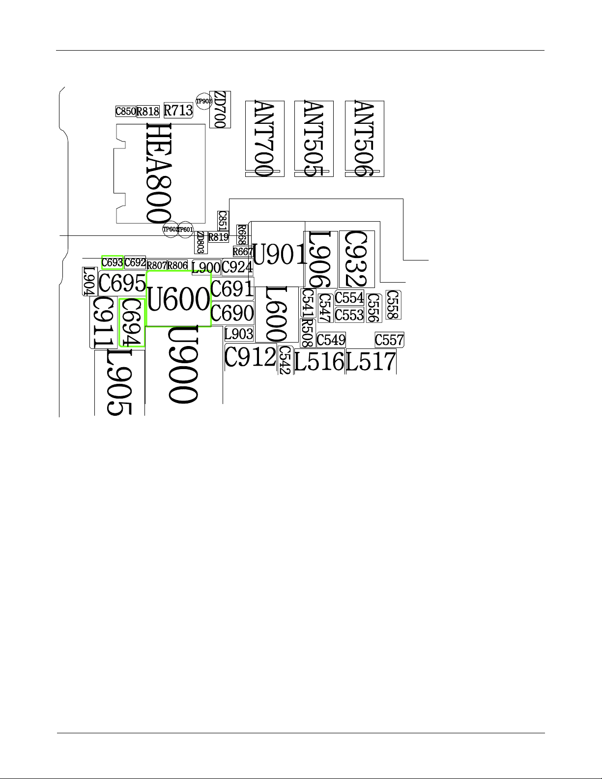
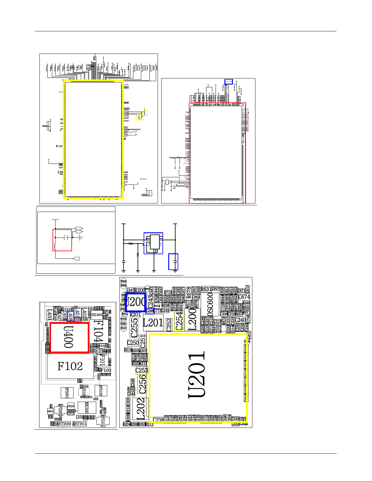
8-3-3.
No Service
No service
Yes
Check memu setting
Menu→setting→More networks
mobile networks→network mode→setting is auto mode
Menu→Phone→Keypad
*#1234#
→
PHONE:G850FXXXX or
PHONE:unknown
BINARY redownload
→
→
check Phone version
PHONE:unknown
PHONE:unknown
→
?
PHONE:G850FXXXX
Check the connection of RF coaxial cable
PHONE:G850FXXXX
SW problem.
Check the voltage level
C248 and L408=HIGH
YES
Check the voltage level
C254 and C256
Check the voltage level
C425
Replace U 400
=1.2V
=1.2V
Yes
(4.0
V)
NO
NO
if yes, resolder or change U200
Replace the U201
END
8-15
Confidential and proprietary-the contents in this service guide subject to change without prior notice.
Distribution, transmission, or infringement of any content or data from this document without Samsung’swritten authorization is strictly prohibited.
Level3Repair
_
N
CP_VSD2_1.8V
CP_VSD2_1.8V
0
1
0
0
2
2
C
C
CP_VSD3_1.2V
CP_VSD3_1.2V
CP_VSD2_1.8V
VRTC_1.8V
CP_VSD1_1.0V
CP_VSD1_1.0V
7
0
2
C
CP_VSD2_1.8V
3
4
0
0
2
2
R
R
HW_ID1_CP
HW_ID2_CP
HW_ID3_CP
8
6
0
0
2
2
R
R
CP_VSD2_1.8V
CP_VSD2_1.8V
CP_VSD1_1.0V
CP_VSD1_1.0V
CP_VSD1_1.0V
9
0
8
1
0
1
0
6
7
2
2
1
2
3
3
2
C
C
C
2
2
C
C
C
USB_VBUS_CP_4.9V
DDR_CKE
HW_MON1
HW_MON2
COEX_CP_TXD
COEX_CP_RXD
HW_ID1_CP
HW_ID2_CP
5
0
2
R
HW_ID3_CP
TMS_CP
7
0
2
R
R212
TH200
3
1
2
R
TP209
SPEECH_PCM_CLK
TP210
SPEECH_PCM_IN_CP
TP211
SPEECH_PCM_OUT_CP
TP212
SPEECH_PCM_SYNC
LLI_CLK_REQ
RGB_G_EN
TP213
PHONE_ACTIVE
C257
C258
RFE_MPHY_SYS_CLK_EN
RFE_MPHY2_SYS_CLK_EN
RFE_MPHY_RX1_DATX
RFE_MPHY_RX2_DATX
RFE_MPHY_RX1_DAT
RFE_MPHY_RX2_DAT
RFE_MPHY2_RX1_DATX
RFE_MPHY2_RX2_DATX
RFE_MPHY2_RX1_DAT
RFE_MPHY2_RX2_DAT
CP_VSD3_1.2V
CP_VSD2_1.8V CP_VSD2_1.8V
3
8
6
7
9
1
2
0
3
0
2
2
2
2
3
3
3
3
2
2
2
2
2
2
2
2
2
2
C
C
C
C
1
2
C
C249
C250
1
C
A
S
U
B
V
AC11
DDR_CA_0
AD11
DDR_CA_1
AE10
DDR_CA_2
AH11
DDR_CA_3
AD10
DDR_CA_4
AG9
DDR_CA_5
AH10
DDR_CA_6
AF11
DDR_CA_7
AH9
DDR_CA_8
AG10
DDR_CA_9
AG12
DDR_CK_C
AH12
DDR_CK_T
AF8
DDR_CKE_0
AF9
DDR_CKE_1
AF10
DDR_CS_0
AE9
DDR_CS_1
AC20
DDR_DQ_0
AB20
DDR_DQ_1
AD16
DDR_DQ_2
AD17
DDR_DQ_3
AD19
DDR_DQ_4
AA20
DDR_DQ_5
AC19
DDR_DQ_6
AC18
DDR_DQ_7
AE16
DDR_DQ_8
AB15
DDR_DQ_9
AA15
DDR_DQ_10
AE15
DDR_DQ_11
AD14
DDR_DQ_12
AF15
DDR_DQ_13
AA14
DDR_DQ_14
AB14
DDR_DQ_15
AH15
DDR_DQ_16
AH16
DDR_DQ_17
AG20
DDR_DQ_18
AH19
DDR_DQ_19
AH18
DDR_DQ_20
AG19
DDR_DQ_21
AG16
DDR_DQ_22
AH17
DDR_DQ_23
AC13
DDR_DQ_24
AD13
DDR_DQ_25
AF13
DDR_DQ_26
AB12
DDR_DQ_27
AC12
DDR_DQ_28
AF12
DDR_DQ_29
AG13
DDR_DQ_30
AB11
DDR_DQ_31
AA18
DDR_DQM_0
AB17
DDR_DQM_1
AE18
DDR_DQM_2
AF14
DDR_DQM_3
AB18
DDR_DQS_C_0
AC16
DDR_DQS_C_1
AE19
DDR_DQS_C_2
AH14
DDR_DQS_C_3
AB19
DDR_DQS_T_0
AB16
DDR_DQS_T_1
AF19
DDR_DQS_T_2
AG14
DDR_DQS_T_3
J9
HW_MON1
M7
HW_MON2
L5
HW_MON17
H5
HW_MON18
F5
HW_MON19
H17
HW_MON20
H18
HW_MON21
H15
HW_MON22
G18
HW_MON23
L9
HW_MON24
J11
HW_MON25
G5
HW_MON26
K18
HW_MON27
M9
HW_MON28
M10
HW_MON29
M5
HW_MON30
L6
HW_MON31
K5
HW_MON32
J10
TMS
D12
TM_EN
A1
DUMMY_BALL
A2
DUMMY_BALL
A3
DUMMY_BALL
A4
DUMMY_BALL
A5
DUMMY_BALL
A6
DUMMY_BALL
A7
DUMMY_BALL
A20
DUMMY_BALL
AH1
DUMMY_BALL
AH20
DUMMY_BALL
B1
DUMMY_BALL
B2
DUMMY_BALL
B3
DUMMY_BALL
B4
DUMMY_BALL
B5
DUMMY_BALL
B6
DUMMY_BALL
B7
DUMMY_BALL
C1
DUMMY_BALL
C2
DUMMY_BALL
C3
DUMMY_BALL
C4
DUMMY_BALL
C5
DUMMY_BALL
D1
DUMMY_BALL
D2
DUMMY_BALL
D3
DUMMY_BALL
D4
DUMMY_BALL
E12
M1
F11
M2
D9
M3
E11
M4
AF7
NAND_ADQ_0
AH6
NAND_ADQ_1
AC6
NAND_ADQ_2
AE7
NAND_ADQ_3
AH7
NAND_ADQ_4
AD3
NAND_ADQ_5
AD7
NAND_ADQ_6
AC8
NAND_ADQ_7
AD5
NAND_ADQ_8
AG6
NAND_ADQ_9
AC4
NAND_ADQ_10
AE5
NAND_ADQ_11
AD6
NAND_ADQ_12
AE8
NAND_ADQ_13
AF4
NAND_ADQ_14
AC5
NAND_ADQ_15
AH5
NAND_ALE
AE6
NAND_CE
AB6
NAND_CLE
AB5
NAND_CLK_X_IN
AA4
NAND_CLK_X_OUT
AB8
NAND_RB
AG5
NAND_RE
AF6
NAND_WE
AF5
NAND_WP
N8
I2C1_SCL
N7
I2C1_SDA
R6
I2S1_CLK0
P4
I2S1_CLK1
N5
I2S1_RX
R4
I2S1_TX
N4
I2S1_WA0
P5
I2S1_WA1
N11
I2C2_SCL
N10
I2C2_SDA
J6
I2S2_CLK0
AA2
I2S2_CLK1
L7
I2S2_RX
M6
I2S2_TX
M8
I2S2_WA0
AB2
I2S2_WA1
AG11
DDR_VREF_CA
AD9
DDR_VREF_CA_M
AC15
DDR_VREF_DQ
Y15
DDR_VREF_DQ_M
L1
DIGRF1EN
Y2
DIGRF2EN
P3
LDO_MON_DIGRF1
U3
LDO_MON_DIGRF2
AG15
LDO_MON_EMIC
U17
LDO_MON_PCIE
Y13
LDO_MON_PLL
N20
LDO_MON_SSIC
AD2
LDO_MON_USB_HSIC
AH4
LDO_MON_USB_SS
W17
PCI_PER
V17
PCI_PER_P1
W19
PCI_PET
Y19
PCI_PET_P1
Y17
PCI_REFCLK
AA17
PCI_REFCLK_P
AA16
PCI_REF_RES
P11
RCT_MON
R11
RCT_MON
G19
RESERVED_1
F19
RESERVED_2
A9
RESERVED_3
G20
RESERVED_4
N2
RXDATA1NLANE1
M1
RXDATA1NLANE2
N1
RXDATA1PLANE1
M2
RXDATA1PLANE2
V1
RXDATA2NLANE1
W1
RXDATA2NLANE2
V2
RXDATA2PLANE1
Y1
RXDATA2PLANE2
S
S
S
S
S
S
S
S
S
S
S
S
S
S
V
V
V
V
V
V
V
4
9
2
8
3
7
9
1
1
E
D
A
C
B
C
A
A
A
A
A
A
A
A
4
5
3
1
2
C
C
C
C
C
2
2
2
2
2
2
2
2
2
2
C
C
C
C
C
7
8
3
3
1
1
5
8
2
0
3
7
2
1
6
0
5
4
5
2
3
4
0
5
1
4
1
2
4
0
1
1
9
7
1
1
1
1
1
9
6
9
7
2
9
1
1
4
8
1
1
1
1
1
1
1
1
1
1
1
D
G
1
1
F
B
L
E
G
E
D
C
Y
Y
U
R
B
A
A
P
P
N
D
C
T
T
T
V
S
_
S
B
E
B
_
_
R
P
P
O
C
C
C
V
V
_
D
D
V
R
N
L
K
D
D
A
U
A
J
W
W
U
U
R
Y
Y
V
N
L
L
A
A
A
A
A
A
A
A
A
A
A
A
A
2
8
8
8
3
8
8
1
0
8
E
E
E
E
E
E
E
1
P
N
N
G
N
A
N
G
G
G
O
N
N
O
C
_
I
I
_
I
I
_
_
I
I
I
V
V
V
I
V
V
V
I
T
T
3
3
3
3
T
T
T
Y
S
T
T
C
_
A
1
1
A
1
A
_
1
1
A
1
A
A
O
L
L
O
_
_
_
_
I
L
L
O
O
L
L
L
_
H
M
D
I
I
I
I
_
_
_
8
_
_
_
_
_
_
_
_
_
_
M
M
M
M
E
E
E
E
_
S
M
M
_
_
E
_
_
P
O
V
_
O
E
O
_
E
O
O
_
_
O
E
O
I
E
E
_
E
E
_
R
R
_
R
_
R
E
H
C
I
I
I
C
I
I
I
C
C
1
I
I
_
I
I
E
R
E
R
E
E
_
R
R
E
R
R
R
E
_
_
_
_
_
_
F
E
R
_
O
O
O
O
C
M
R
R
M
R
R
M
D
M
R
R
D
O
D
O
D
D
D
O
O
O
D
R
I
O
R
O
C
C
C
C
C
O
I
E
E
D
E
E
O
D
C
D
O
C
D
D
D
O
_
C
C
D
O
O
_
_
_
C
C
C
O
G
O
M
C
_
_
_
_
I
_
_
_
_
M
_
_
_
V
C
V
V
C
V
V
C
C
V
D
D
D
_
D
V
C
C
C
E
D
D
D
D
D
_
D
_
D
_
D
_
E
D
D
_
D
D
_
_
_
D
D
D
D
D
_
D
D
_
D
D
D
D
D
D
D
D
D
D
D
D
D
D
D
D
V
V
V
D
V
O
V
V
V
V
D
O
D
V
D
V
D
V
D
V
V
D
V
V
D
D
V
D
D
D
V
V
V
V
V
V
L
V
L
V
_
_
D
D
D
D
V
V
U201
S
S
S
S
S
S
S
S
S
S
V
V
V
V
7
3
4
4
1
1
6
E
G
E
H
C
A
A
A
A
S
S
S
S
S
S
S
S
S
S
S
S
S
S
S
S
S
S
S
S
S
S
S
S
S
S
S
S
S
S
S
S
S
S
S
S
S
S
S
S
S
S
S
S
S
S
S
S
S
S
S
S
S
S
S
S
S
S
S
S
S
S
S
S
V
V
V
V
V
V
V
V
V
V
V
V
V
V
V
V
V
V
V
V
V
V
V
V
V
V
V
V
V
V
V
V
V
6
6
7
9
6
0
7
3
1
4
2
0
9
8
3
0
5
3
6
1
5
0
3
4
9
1
5
7
7
6
7
3
3
1
1
1
1
1
1
1
1
1
1
1
1
1
1
1
1
1
1
1
1
1
1
1
J
J
L
P
M
K
D
C
D
D
J
J
F
M
P
K
K
K
H
G
E
E
D
D
C
C
C
K
K
D
E
H
H
VUSB_IO_3.1V
CP_VSIM_2.9V
CP_VSD3_1.2V
CP_VSD3_1.2V
VRTC_1.8V
VPH_PWR_CP
CP_VSIM_2.9V
D
N
G
4
_
C
S
O
4
3
3
2
1
C
2
C
1
2
D
D
S
S
V
V
_
_
N
N
I
I
V
V
_
_
D
D
D
D
V
V
7
3
4
9
6
3
8
2
2
7
8
1
1
8
0
9
9
1
6
1
1
1
1
1
1
2
1
1
E
B
A
H
G
B
A
G
P
K
D
C
Y
V
D
A
A
V
A
A
A
A
A
A
A
A
8
1
1
2
L
2
C
O
U
O
O
E
O
O
S
C
I
O
I
I
I
I
C
I
V
L
I
D
I
D
D
Y
I
T
_
M
S
_
_
_
_
1
C
_
P
S
S
S
S
H
R
2
1
_
M
P
_
C
S
B
P
_
_
C
_
_
H
_
P
_
I
B
E
M
E
_
M
S
M
M
_
I
N
I
N
N
I
O
_
D
_
I
N
S
I
I
_
S
I
O
S
B
S
M
C
F
S
D
L
D
V
H
V
V
U
B
_
_
V
D
_
_
L
L
S
P
R
V
_
_
_
_
_
S
_
L
_
D
D
D
D
_
D
U
D
B
D
D
G
_
O
U
D
D
I
D
_
_
D
D
D
D
D
S
D
D
_
D
D
D
D
D
V
V
D
V
V
O
O
V
U
V
V
L
D
D
_
V
V
V
D
D
_
_
D
V
O
L
L
D
D
V
_
_
D
D
D
D
L
D
V
V
_
D
D
D
V
V
D
V
M
M
E
E
M
M
_
_
Q
Q
S
S
S
S
S
S
S
S
S
S
S
S
S
S
S
S
S
S
S
S
S
S
S
S
S
S
S
S
S
S
S
S
S
S
V
V
V
V
V
V
V
V
V
V
V
V
V
V
V
V
V
0
1
9
2
9
0
5
0
6
0
0
3
4
2
7
1
5
4
8
1
1
1
1
2
1
2
1
2
1
1
F
T
R
Y
U
T
T
U
W
V
V
U
P
P
K
U
V
A
D
N
G
_
C
S
O
D
0
N
2
C
G
2
A
0
2
C
5
3
5
2
C
2
3
4
4
2
2
C
C
3
D
S
V
_
N
I
V
_
D
D
V
0
8
9
5
0
9
0
8
5
3
0
3
0
0
9
2
1
1
9
8
1
1
1
2
2
1
2
1
2
G
A
H
2
J
F
E
H
B
A
J
H
C
Y
P
L
F
B
A
R
A
A
A
A
6
2
P
F
1
2
U
C
3
M
M
M
M
M
M
M
M
M
M
V
P
E
Y
D
M
T
M
M
D
E
E
I
E
E
E
E
E
E
E
I
E
0
V
R
H
S
R
P
S
_
S
S
M
M
M
M
M
M
M
M
M
M
V
P
V
_
V
V
F
_
_
_
_
V
_
_
_
_
_
V
_
_
N
M
1
2
1
1
2
2
E
I
Q
Q
Q
Q
D
_
D
D
D
D
D
D
R
V
D
D
D
D
D
C
D
_
D
D
D
D
D
I
V
D
D
D
D
V
V
V
D
V
V
V
V
S
V
V
V
V
D
S
_
V
B
S
U
_
O
D
L
_
D
D
V
X
X
T
R
_
_
N
N
C
C
I
I
I
I
X
X
A
A
S
S
U
U
X
S
M
S
A
A
M
_
_
_
_
_
_
T
M
M
_
Y
Y
Y
Y
Y
Y
C
C
C
C
C
C
C
C
E
E
E
H
I
I
I
H
H
I
H
I
I
I
I
H
H
1
1
2
I
L
L
P
M
P
P
P
M
P
P
M
M
M
D
M
M
M
L
D
L
M
M
D
C
_
_
E
E
E
M
M
M
S
E
M
E
E
P
S
P
E
E
S
M
M
P
_
_
_
_
Q
_
_
_
_
_
_
_
_
_
_
Q
_
_
_
_
_
_
S
S
S
S
S
S
S
S
S
S
S
S
S
S
S
S
S
S
S
S
S
S
S
S
S
S
S
S
S
S
S
S
S
S
S
S
S
S
S
S
S
S
S
S
V
V
V
V
V
V
V
V
V
V
V
V
V
V
V
V
V
V
V
V
V
V
6
8
4
2
7
0
5
3
6
8
9
0
8
9
6
3
6
1
3
1
1
1
1
3
5
2
3
1
1
1
1
2
1
1
A
1
1
F
T
F
E
E
C
V
Y
W
R
T
J
U
N
M
B
B
A
W
A
Y
A
A
A
A
A
D
D
N
N
G
G
_
_
2
1
D
D
S
S
V
V
8
4
0
3
1
2
2
2
C
C
C
6
4
4
4
2
2
C
C
5
4
2
C
R202
TP200
V8
MIPI_HSI_RX_DATA
IPC_HOST_WAKEUP
U6
MIPI_HSI_RX_FLG
W7
TP201
MIPI_HSI_RX_RDY
W6
MIPI_HSI_RX_WAKE
SUSPEND_REQUEST_HSIC
T5
TP202
MIPI_HSI_TX_DATA
CP2AP_WAKE
U5
TP203
MIPI_HSI_TX_FLG
HOST_ACTIVE
V7
TP204
MIPI_HSI_TX_RDY
PDA_ACTIVE
V6
MIPI_HSI_TX_WAKE
U4
MMCI1_CD
T6
MMCI1_CLK
T9
MMCI1_CMD
AA7
MMCI2_CLK
Y8
MMCI2_CMD
AA9
MMCI2_RST
V9
MMCI1_DAT_0
T11
MMCI1_DAT_1
V10
MMCI1_DAT_2
T10
MMCI1_DAT_3
AA10
MMCI2_DAT_0
Y11
MMCI2_DAT_1
W10
MMCI2_DAT_2
W9
MMCI2_DAT_3
K9
USIF1_CTS
G7
USIF1_RTS
K8
USIF3_CTS
J8
USIF3_RTS
H7
USIF1_SCLK
E7
USIF3_SCLK
H8
USIF1_RXD_MRST
UART_RXD_CP
F7
USIF1_TXD_MTSR
UART_TXD_CP
E8
USIF3_RXD_MRST
CP_RXD_1.8V
D8
USIF3_TXD_MTSR
CP_TXD_1.8V
M19
USIF_LTE_TXD
AG2
USB30_RXN
AF2
USB30_RXP
AF1
USB30_TXN
AG1
USB30_TXP
P18
USB_SSIC_RXN
LLI_RX_DN
N17
USB_SSIC_RXP
LLI_RX_DP
R18
USB_SSIC_TXN
LLI_TX_DN
R17
USB_SSIC_TXP
LLI_TX_DP
D17
SD1_FB
C19
SD1_SW
C20
L200
SD1_SW
C17
SD2_FB
A17
SD2_SW
A18
L201
SD2_SW
C11
SD3_FB
A11
L202
SD3_SW
B11
SD3_SW
Y7
SYS_CLK
RFE_SYS_CLK
R8
CC1_IO
SIM_IO
J12
CC2_IO
P8
CC1_CLK
SIM_CLK
N6
CC1_RST
SIM_RST
J13
CC2_CLK
K12
CC2_RST
Y14
CKE_MEM
DDR_CKE
V5
CLKOUT0
GPS_CLK_26M
W5
CLKOUT1
V4
CLKOUT2
V12
EINT1
W13
EINT2
W12
EINT3
R7
DMINUS
P7
DPLUS
G6
DSP_AUDIO_IN1
DSP_AUDIO_IN1
TP205
AC3
HSIC_USB_DATA
HSIC_DATA
TP206
AB3
HSIC_USB_STRB
HSIC_STROBE
AC2
USB_TEST
AD1
USB_DPLUS
AE1
USB_DMINUS
R209
AH3
USB_TUNE
VRTC_1.8V
G9
RESET_RFE
RFE_RESET_MAIN
R210
G11
RESET_ALL
G14
RESET_BB
RESET_REQ_N
H9
TP207
RESET2
R19
RESET_LDO
RFE_RESET_MAIN
CP_VSD2_1.8V
G10
REF_CLK_EN
RFE_REF_CLK_EN
R211
F6
T_OUT0
K6
T_OUT1
H6
T_OUT2
SLAVE_WAKEUP
G8
TP208
T_OUT3
E9
TCK
TCK_CP
E10
TDI
TDI_CP
G4
TDO
TDO_CP
F4
RTCK
RTCK_CP
F15
RTC_ALARM
L13
TD_SDRAM_A0
W14
TD_SDRAM_A1
R15
TD_SDRAM_A2
U15
TD_SDRAM_A3
M12
TD_SDRAM_A4
U14
TD_SDRAM_A5
V15
TD_SDRAM_A6
T15
TD_SDRAM_A7
T16
TD_SDRAM_A8
W15
TD_SDRAM_A9
R16
TD_SDRAM_A10
T14
TD_SDRAM_A11
K15
TD_SDRAM_CASN
L15
TD_SDRAM_CLE
L18
TD_SDRAM_CLK
M17
TD_SDRAM_CSN
P13
TD_SDRAM_D0
P14
TD_SDRAM_D1
P12
TD_SDRAM_D2
N13
TD_SDRAM_D3
P17
TD_SDRAM_D4
L11
TD_SDRAM_D5
N14
TD_SDRAM_D6
L12
TD_SDRAM_D7
M18
TD_SDRAM_D8
M13
TD_SDRAM_D9
N16
TD_SDRAM_D10
P16
TD_SDRAM_D11
M14
TD_SDRAM_D12
M20
TD_SDRAM_D13
T17
TD_SDRAM_D14
K16
TD_SDRAM_D15
L16
TD_SDRAM_DQM0
L17
TD_SDRAM_DQM1
L19
TD_SDRAM_RASN
N18
TD_SDRAM_WEN
J2
TPIU_TRACECLK
G2
TPIU_TRACECTL
G3
TPIU_TRACEPKT0
G1
TPIU_TRACEPKT1
F2
TPIU_TRACEPKT2
H4
TPIU_TRACEPKT3
E3
TPIU_TRACEPKT4
E4
TPIU_TRACEPKT5
E2
TPIU_TRACEPKT6
F1
TPIU_TRACEPKT7
K3
TPIU_TRACEPKT8
K2
TPIU_TRACEPKT9
E1
TPIU_TRACEPKT10
H2
TPIU_TRACEPKT11
J5
TP214
TPIU_TRACEPKT12
AP2CP_STATUS
H3
TPIU_TRACEPKT13
F3
TPIU_TRACEPKT14
AP_DUMP_INT
K4
TPIU_TRACEPKT15
CP_DUMP_INT
F13
TRIG_B
E6
TRIG_IN
TRIG_IN
E5
TRST_n
TRST_N_CP
P2
TXDATA1N
RFE_MPHY_TX_DATX
P1
TXDATA1P
RFE_MPHY_TX_DAT
U1
TXDATA2N
RFE_MPHY2_TX_DATX
U2
TXDATA2P
RFE_MPHY2_TX_DAT
TP216
G12
OFF
RESET_PWRDWN_N
RESET_PWRDWN_N
TP217
D10
ON
CP_ON
T20
OSC32K
U20
F32K
32KHZ_CP
D16
FSS
AGND
B8
AGND
C8
AGND_SENSE
R214
D13
ANAMON
T1
BUS_SET_MEM
M3
TP215
XRESET
RFE_RESET_TRX
AC9
R215
ZQ_MEM
1
MARK
6
2
1
MARK
2
R
E
S
N
3
3
B
O
E
D
D
S
I
_
S
S
S
U
_
_
_
_
B
S
S
S
VUSB_IO_3.1V
S
S
S
S
S
S
U
V
V
V
V
V
3
0
0
4
8
1
1
F
1
F
B
A
A
B
D
N
G
_
3
D
S
V
CP_VSD3_1.2V
6
0
8
0
9
5
1
2
C
CP_VSD3_1.2V
C256
CP_VSD3_1.2V
DSP_AUDIO_IN1
2
7
2
6
1
1
0
1
9
C
2
2
1
2
1
3
4
4
C
C
2
2
C
2
2
2
C
C
C
C
C
VPH_PWR_CP
RFE_VDD_2V5_SDH
RFE_VDD_RFLDO1
RFE_VDD_1V5_SDL
RFE_VDD_2V5_SDH
C411
C410
C405
7
8
6
2
9
0
0
0
1
0
4
4
4
4
4
C
C
C
C
C
2
2
0
0
0
7
8
5
5
9
5
6
6
1
7
5
9
1
7
5
9
1
1
1
1
1
P
T
P
L
L
F
F
F
J
M
N
D
C
D
K
K
U
P
A
C
E
1
2
5
4
3
6
2
3
5
4
7
9
1
8
0
1
2
4
3
1
1
X
X
X
X
X
X
X
X
1
X
X
X
X
X
X
1
X
X
X
X
X
T
T
T
T
T
R
R
R
R
R
R
X
R
T
T
T
R
T
R
X
R
_
_
_
_
_
_
_
_
_
_
_
_
_
_
_
_
_
_
R
_
R
L
L
L
L
L
L
L
L
L
L
L
L
1
1
1
L
1
L
_
1
_
D
D
D
D
D
D
L
D
D
D
D
D
D
H
H
H
D
H
D
L
H
D
D
D
D
D
D
D
D
D
D
D
D
D
D
D
D
D
D
D
D
D
V
V
V
V
V
V
D
V
V
V
V
V
V
D
D
D
V
D
V
D
CP_VSD1_1.0V
CP_VSD2_1.8V
C254
C255
VSD2_GND
VSD3_GND
USB_DP_CP
USB_DM_CP
FBR_REV
FBR_FWD
ANT_SWITCH_SEL_MAIN
RFE_RFFE2_SDATA
RFE_RFFE2_SDATA_PA
4
5
0
0
4
4
L
L
DRX_HB_LNA_EN
DRX_MB_LNA_EN
CPL_SWITCH_SEL
DRX_LB_LNA_EN
RFE_RFFE2_VIO
PRX_B7_LNA_EN
ANT_SWITCH_SEL_SUB
RFE_RFFE2_SCLK
RFE_RFFE2_SCLK_PA
OSC400
CP_PMU_RST
CP_VSD2_1.8V
R220
R219R217
R218
HW_MON1
HW_MON2
TRIG_IN
RFE_PADACF_100D_P
RFE_PADACF_100D_N
N
C
4
1
O
C
C
V
V
T
D
3
2
RFE_VDDIO
U
N
O
G
VPH_PWR_CP
4
5
3
3
4
C
RFE_PADCDC_MI
4
C
D
V
V
V
V
V
V
V
W3
RD_H1
W2
RD_H1X
V4
RD_H2
V3
RD_H2X
W5
RD_H3
DIV_RXB7
W4
RD_H3X
DIV_RXB7X
W8
RD_M5
W9
RD_M5X
V5
RD_M2
DIV_RXB2
V6
RD_M2X
DIV_RXB2X
W6
RD_M3
DIV_RXB3
W7
RD_M3X
DIV_RXB3X
V7
RD_M4
DIV_RXB1_4
V8
RD_M4X
DIV_RXB1_4X
V12
RD_L1
DIV_RXB20
V11
RD_L1X
DIV_RXB20X
W13
RD_L2
W12
RD_L2X
W11
RD_L3
DIV_RXB5
W10
RD_L3X
DIV_RXB5X
V10
RD_L4
DIV_RXB8
V9
RD_L4X
DIV_RXB8X
R2
RX_H1
RXB1
P2
RX_H1X
RXB1X
T1
RX_H2
R1
RX_H2X
U2
RX_H3
T2
RX_H3X
V1
RX_H4
RXB7
U1
RX_H4X
RXB7X
P1
RX_M1
N1
RX_M1X
N2
RX_M2
M2
RX_M2X
M1
RX_M3
RXB3
L1
RX_M3X
RXB3X
L2
RX_M4
RXB4
K2
RX_M4X
RXB4X
K1
RX_M5
RXB2
J1
RX_M5X
RXB2X
F2
RX_L1
RXB20
G2
RX_L1X
RXB20X
E1
RX_L2
RXB17
F1
RX_L2X
RXB17X
G1
RX_L3
RXB5
H1
RX_L3X
RXB5X
H2
RX_L4
RXB8
J2
RX_L4X
RXB8X
A5
TQ_T
B3
TQ_X
HB7_TX
A4
TQ_M
B5
TQ_L
LTE_LB_TX
B4
TQ_H
LTE_MB_TX
C10
TP_H
2G3G_HB_TX
C8
TP_L
2G3G_LB_TX
C431C430
A11
FBR_RF1
A13
C433C432
FBR_RF2
E13
RFFE_VIO
E14
RFFE_SCLK
F15
RFFE2_SDATA
L406
G12
SPI_VSPI
G13
SPI_CLK
G15
SPI_SS
G14
SPI_DRW
J7
GPO0
H6
GPO1
G6
GPO2
H5
GPO3
E4
GPO4
DRX_SW_SEL2
B1
GPO5
H13
GPO6
DRX_SW_SEL0
H14
GPO7
DRX_SW_SEL1
H15
GPO8
E15
RFFE_SDATA
F14
RFFE2_SCLK
F13
RFFE2_VIO
L407
C11
PADACS
D12
PADACF_P
D11
PADACF_N
U15
AFC_DAC
W16
XO_SUP
V18
XO
R14
CONF1
R12
MI1
R13
R401
MI2
P14
MI3
W15
TAS_RX
V15
TAS_TX
1
MARK
2
MARK
S
S
S
S
S
S
S
S
S
S
S
S
S
S
S
S
S
S
S
S
S
S
S
S
S
S
S
S
S
S
S
S
S
S
S
S
S
S
S
S
S
S
S
S
S
S
V
V
V
V
V
V
V
V
V
V
V
V
V
V
V
V
V
V
V
V
V
V
V
3
2
1
3
0
2
5
3
2
5
3
2
9
8
9
6
6
9
7
6
5
4
3
2
1
1
1
1
1
1
1
E
E
E
A
D
D
B
C
B
A
B
C
C
C
C
C
C
B
B
B
D
B
A
D
L408
RFE_VDD_1V2_SDD
RFE_VDDIO
RFE_VDD_1V5_SDL
6
3
4
5
1
1
1
1
4
7
4
4
4
2
1
C
C
2
C
C
4
4
C
C
6
6
6
2
6
3
4
6
3
2
2
7
8
1
1
1
1
1
1
1
1
1
A
B
D
D
V
P
T
U
L
E
J
K
K
2
2
G
2
I
H
H
2
1
2
3
1
E
E
H
Y
D
D
D
N
O
N
N
N
F
R
I
R
B
I
I
I
_
D
D
D
R
A
A
S
A
A
O
O
D
V
V
L
_
C
M
C
D
M
G
M
M
F
I
D
_
_
_
_
V
G
G
R
D
I
I
D
L
1
1
1
_
_
D
D
V
D
H
H
H
D
8
_
_
D
D
D
D
D
V
D
D
V
D
D
D
1
V
D
D
V
V
V
D
V
V
D
V
U400
S
S
S
S
S
S
S
S
S
S
S
S
S
S
S
S
S
S
S
S
S
S
S
S
S
S
S
S
S
S
S
S
S
S
V
V
V
V
V
V
V
V
V
V
V
V
V
V
V
V
V
0
1
2
1
0
9
8
7
6
5
8
9
4
7
3
8
3
1
1
1
1
1
E
E
E
E
F
F
G
G
G
G
G
G
F
F
F
E
G
RFE_VDD_RFLDO1
C401
C403
2
0
4
C
4
SDL_STARPOINT
0
4
C
T
T
T
N
N
N
I
I
I
O
O
O
P
P
P
R
R
R
0
9
1
8
L
D
2
A
1
A
2
1
A
D
D
4
4
4
4
T
T
H
L
D
T
C
C
C
C
S
0
S
S
S
D
S
D
D
0
_
_
_
_
_
4
S
S
S
L
L
H
D
W
W
_
_
_
3
4
D
D
S
D
S
B
B
B
2
2
S
F
F
S
V
S
4
4
V
F
C
C
7
6
7
8
3
8
7
4
5
4
8
8
7
4
5
7
4
6
6
8
0
7
7
8
7
7
8
1
1
1
1
1
1
1
1
1
1
1
1
1
1
1
1
1
1
1
1
1
1
1
1
R
H
K
C
C
B
B
C
F
E
A
A
U
E
D
D
B
B
A
D
B
A
C
D
F
G
G
S
L
L
L
O
D
T
1
O
H
H
2
1
2
S
H
H
H
H
1
L
2
1
H
D
4
1
2
3
D
D
D
D
X
D
A
D
D
D
X
X
X
V
D
D
T
D
D
H
T
U
U
T
N
N
N
S
S
O
S
T
T
I
I
S
S
B
R
I
S
S
S
F
R
S
S
A
S
S
A
A
_
M
M
_
_
_
_
D
_
_
_
_
_
_
_
_
_
_
A
A
A
_
_
R
B
B
B
S
P
P
T
T
L
T
B
T
2
B
S
D
B
S
1
W
_
D
_
D
M
M
_
M
W
_
_
_
F
S
F
X
X
F
X
F
X
S
D
S
S
D
D
D
_
_
_
D
W
D
S
T
T
W
D
R
V
E
E
E
E
L
L
V
V
L
V
D
V
D
V
S
D
C
C
C
C
D
D
D
V
V
D
D
D
V
V
V
S
S
S
S
S
S
S
S
S
S
S
S
S
S
S
S
S
S
S
S
S
S
S
S
V
V
V
V
V
V
V
V
V
V
V
V
1
6
2
1
0
6
4
3
9
8
4
3
1
1
1
1
1
1
J
J
H
H
H
H
G
H
H
G
H
H
TP401
X
X
S
D
_
V
E
E
V
D
C
C
D
U17
V
SYS_CLK
RFE_SYS_CLK
R18
REF_CLK_EN
RFE_REF_CLK_EN
T18
FSYS1
U18
FSYS1_EN
R17
TP400
FSYS2
LLI_26M_CLK
T17
FSYS2_EN
LLI_CLK_REQ
M14
RESET_TRX_N
RFE_RESET_TRX
L14
RESET_MAIN_N
RFE_RESET_MAIN
P17
MPHY2_SYS_CLK_EN
RFE
MPHY2_SYS_CLK_E
H18
MPHY_RX1_DAT
RFE_MPHY_RX1_DAT
J18
MPHY_RX1_DATX
RFE_MPHY_RX1_DATX
H17
MPHY_RX2_DAT
RFE_MPHY_RX2_DAT
J17
MPHY_RX2_DATX
RFE_MPHY_RX2_DATX
K18
MPHY_TX_DAT
RFE_MPHY_TX_DAT
L18
MPHY_TX_DATX
RFE_MPHY_TX_DATX
P18
MPHY_SYS_CLK_EN
RFE_MPHY_SYS_CLK_EN
N18
MPHY2_RX1_DAT
RFE_MPHY2_RX1_DAT
M18
MPHY2_RX1_DATX
RFE_MPHY2_RX1_DATX
N17
MPHY2_RX2_DAT
RFE_MPHY2_RX2_DAT
M17
MPHY2_RX2_DATX
RFE_MPHY2_RX2_DATX
L17
MPHY2_TX_DAT
RFE_MPHY2_TX_DAT
K17
MPHY2_TX_DATX
RFE_MPHY2_TX_DATX
M15
VDD_TEST
L15
VDD_TEST2
M13
TEST0
N13
TEST1
P13
TEST2
N14
CONF0
W14
NC
A1
NC
A18
NC
W1
NC
W18
NC
R16
NC
W17
NC
V14
NC
L5
VSS
L7
VSS
L8
VSS
L10
VSS
L11
VSS
L12
VSS
L13
VSS
M3
VSS
M4
VSS
M5
VSS
M7
VSS
M9
VSS
M10
VSS
M11
VSS
M12
VSS
M16
VSS
N3
VSS
N4
VSS
N7
VSS
N8
VSS
N9
VSS
N10
VSS
N11
VSS
N12
VSS
N15
VSS
N16
VSS
P3
VSS
P4
VSS
P8
VSS
P9
VSS
P11
VSS
P12
VSS
P15
VSS
R3
VSS
R4
VSS
R5
VSS
R6
VSS
R8
VSS
R9
VSS
R10
VSS
R11
VSS
R15
VSS
T3
VSS
T4
VSS
T6
VSS
T7
VSS
T8
VSS
T9
VSS
T10
VSS
T11
VSS
T12
VSS
T13
VSS
T15
VSS
T16
VSS
U3
VSS
U4
VSS
U5
VSS
U6
VSS
U7
VSS
U8
VSS
U9
VSS
U10
VSS
U11
VSS
U13
VSS
V2
VSS
V13
VSS
V17
VSS
S
S
S
S
S
S
S
S
S
S
S
S
S
S
S
S
S
S
S
S
S
S
S
S
S
S
S
S
S
S
S
S
S
S
S
S
S
S
S
S
V
V
V
V
V
V
V
V
V
V
V
V
V
V
V
V
V
V
V
V
1
0
5
4
2
2
1
0
6
5
4
4
9
4
3
3
6
5
8
1
1
1
1
1
1
1
1
1
1
1
J
L
J
L
J
K
K
K
J
J
J
J
J
J
K
K
K
K
K
RFE_VDD_1V2_SDD
C425
1
0
4
L
FB_SDD
SDD_STARPOINT
VSW_SDD
VPH_PWR
V
3
.
6
VPH_PWR_CP
U200
A2
B3
OUT
IN
A3
C2
OUT
IN
B2
C3
OUT
IN
A1
#EN
B1
R200
1%
R201
%
1
C247
1
MARK
#ACOK
C1
2
MARK
OVLO
D
D
D
N
N
N
G
G
G
4
4
4
C
A
B
C248
V
3
.
6
8-16
Confidential and proprietary-the contents in this service guide subject to change without prior notice.
Distribution, transmission, or infringement of any content or data from this document without Samsung’swritten authorization is strictly prohibited.
Level3Repair
8-3-4.
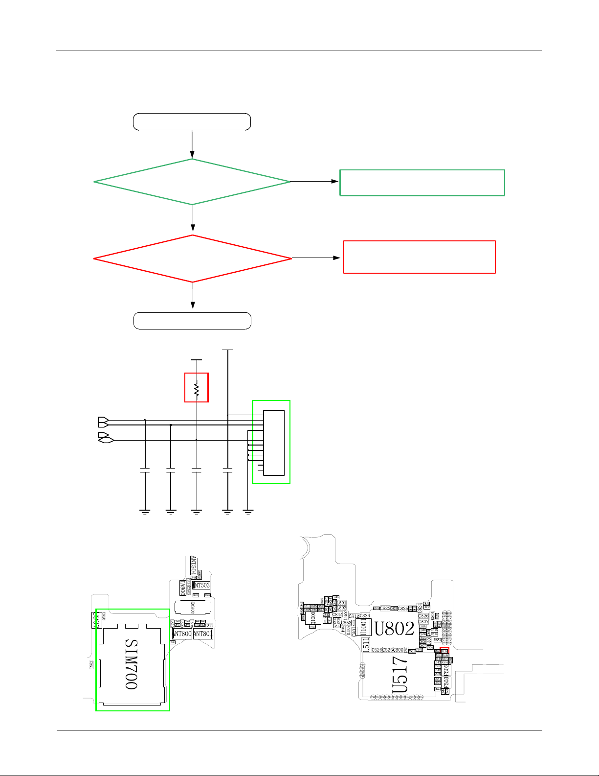
Sim Part
Insert SIM card
Yes
Check the connection of
SIM700
Yes
Check the SIM Voltage.
R712
1.8or3.0?
Yes
END
NFC_SIMVCC
CP_VSIM_2.9V
No
No
Connect SIM FPCB again
Replace the SIM FPCB
SIM_RST
SIM_CLK
NFC_SWP
SIM_IO
R712
C793
C792
C791 C789
S1
S2
S3
S4
S5
S6
G1
G2
G3
G4
SIM700
VCC
RST
CLK
GND
VPP
I|O
GND1
GND2
GND3
GND4
1
NO_GND
2
NO_GND
8-17
Confidential and proprietary-the contents in this service guide subject to change without prior notice.
Distribution, transmission, or infringement of any content or data from this document without Samsung’swritten authorization is strictly prohibited.
Level3Repair
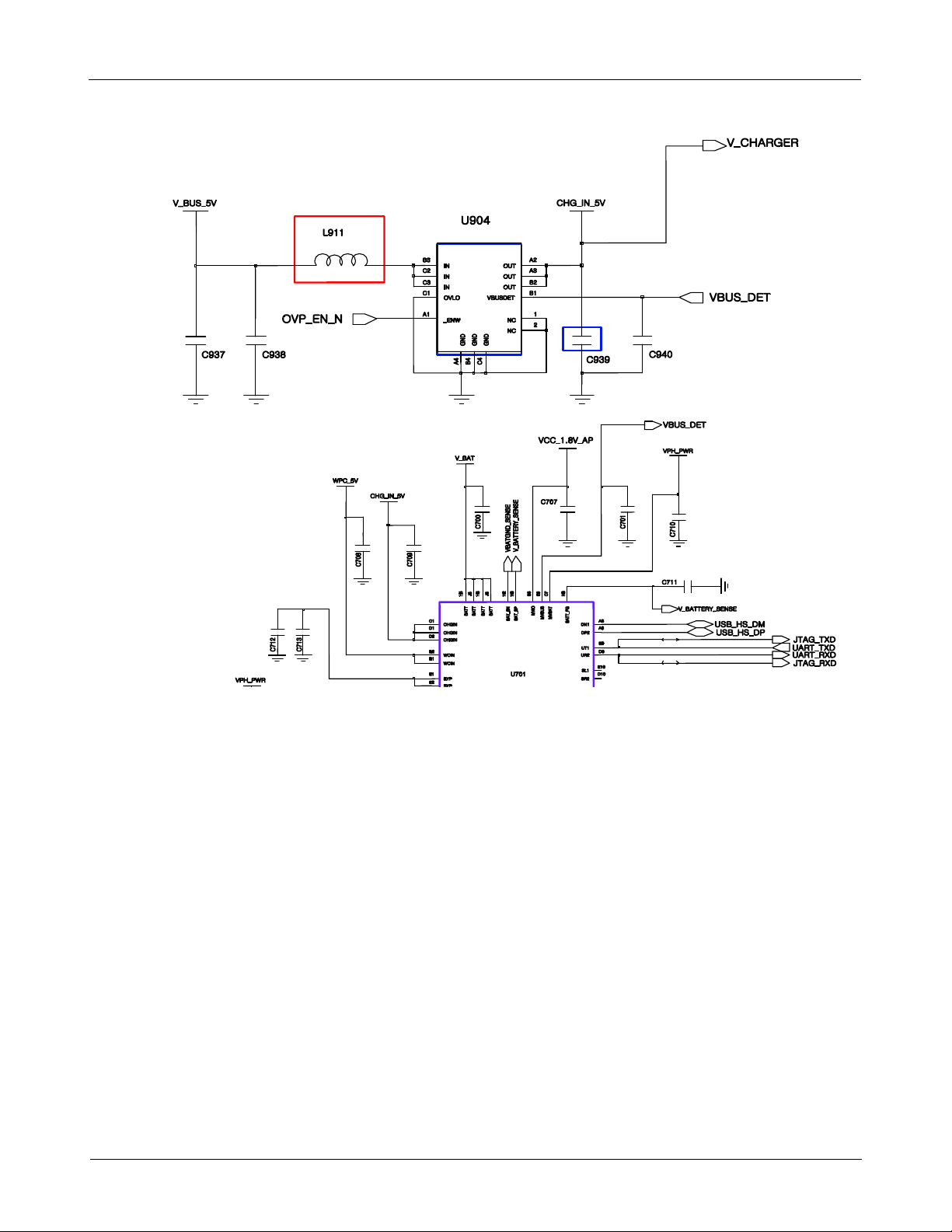
8-3-5.
Charging Part
TA/USB Insert
Charging Sequence Start
V_BUS_5V
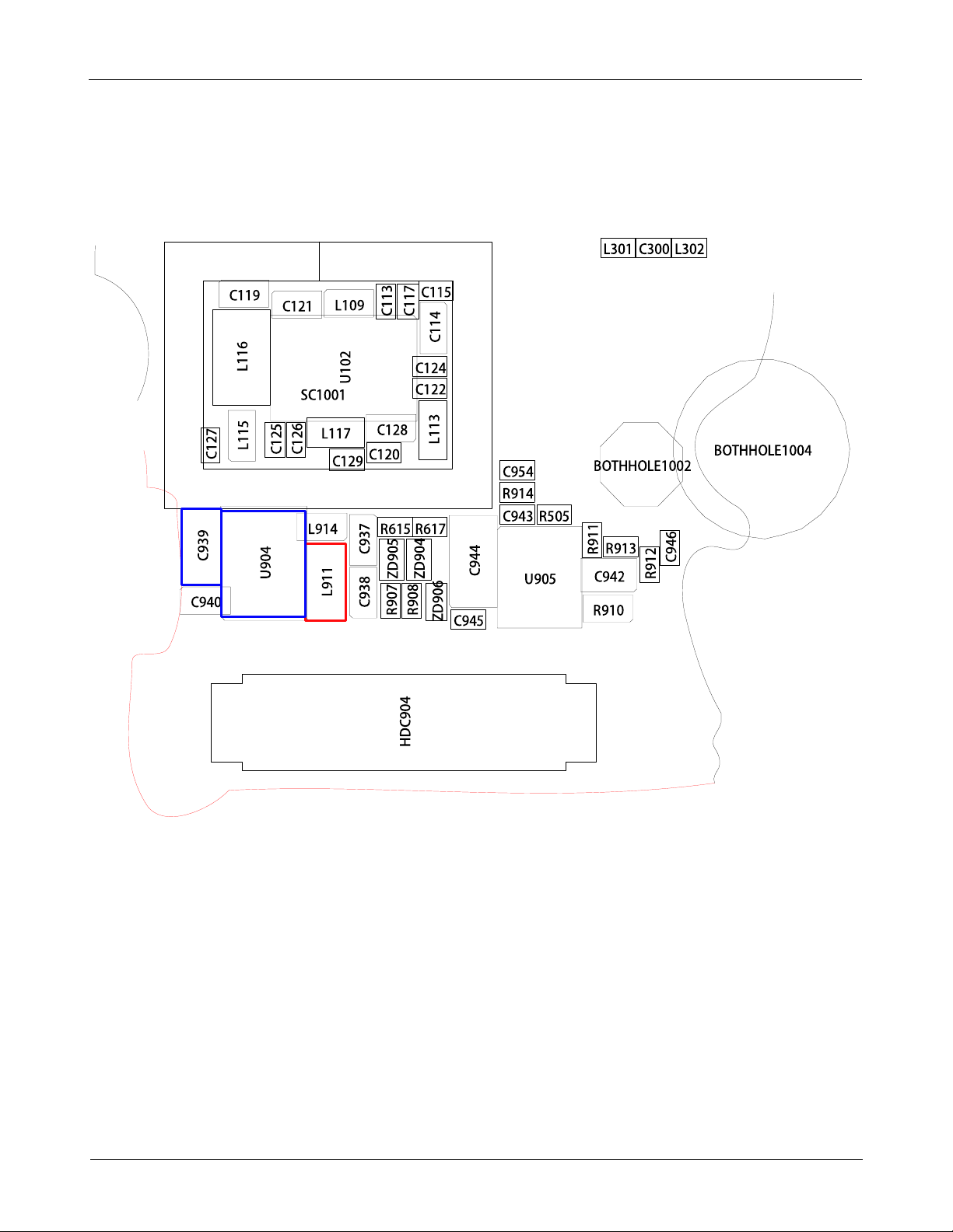
Check the CHG_IN_5V(C939)=5V
Battery is Charging?
Yes
Yes
Yes
Yes
=5V
No
No
No
Check L911=5V,
or may not connected TA/USB
Resolder and Replace U904
Resolder or Replace U701
END
8-18
Confidential and proprietary-the contents in this service guide subject to change without prior notice.
Distribution, transmission, or infringement of any content or data from this document without Samsung’swritten authorization is strictly prohibited.

Level3Repair
8-19
Confidential and proprietary-the contents in this service guide subject to change without prior notice.
Distribution, transmission, or infringement of any content or data from this document without Samsung’swritten authorization is strictly prohibited.

Level3Repair
8-20
Confidential and proprietary-the contents in this service guide subject to change without prior notice.
Distribution, transmission, or infringement of any content or data from this document without Samsung’swritten authorization is strictly prohibited.
Level3Repair
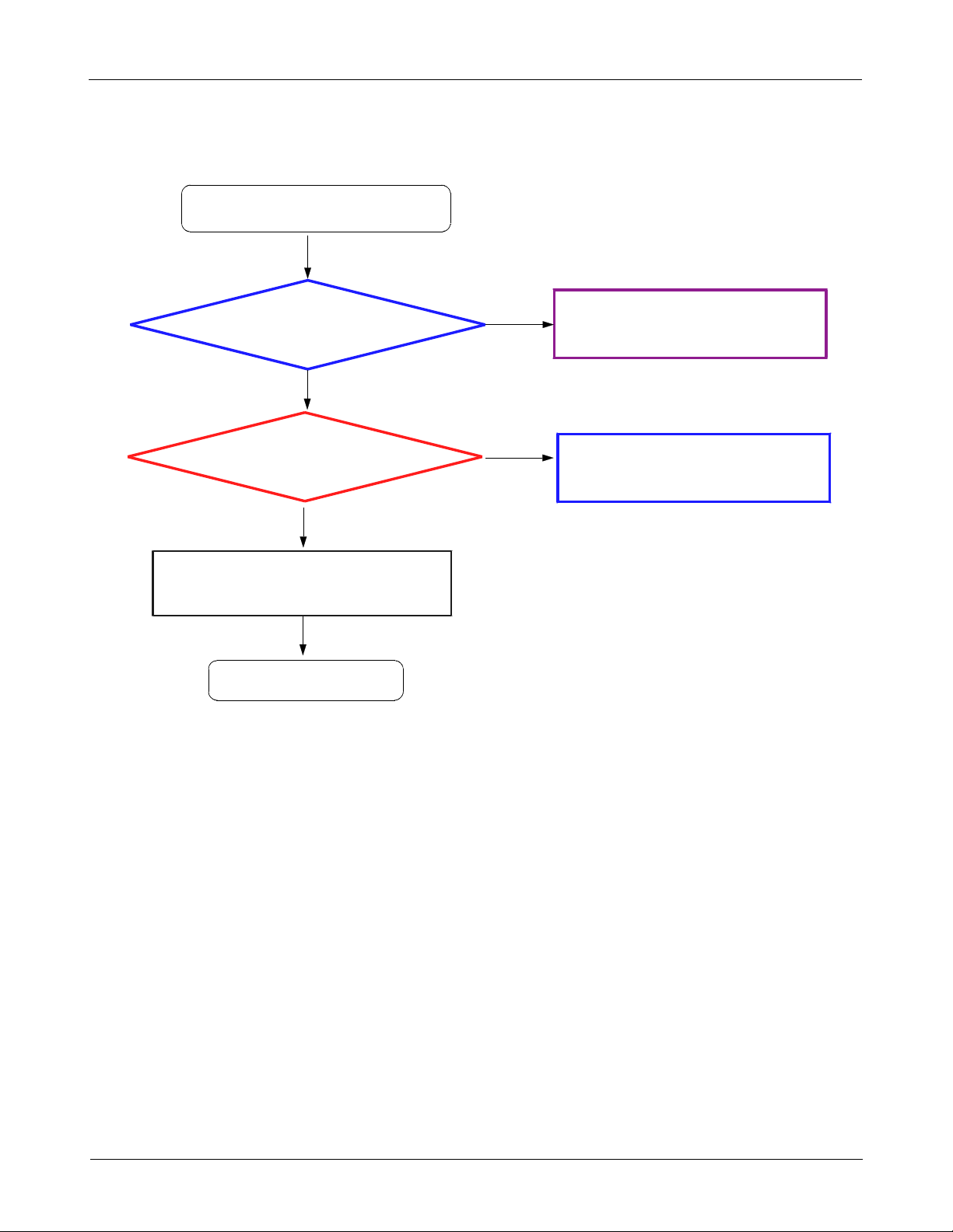
8-3-6.
OTG
OTG does not work
Yes
Check CHG_IN_5V(C939)=5V
Yes
Check V_BUS _5V(L911)
Yes
Change the board
=5V
No
No
Check U701
Check U904
END
Yes
8-21
Confidential and proprietary-the contents in this service guide subject to change without prior notice.
Distribution, transmission, or infringement of any content or data from this document without Samsung’swritten authorization is strictly prohibited.
Level3Repair
8-22
Confidential and proprietary-the contents in this service guide subject to change without prior notice.
Distribution, transmission, or infringement of any content or data from this document without Samsung’swritten authorization is strictly prohibited.
Level3Repair
8-23
Confidential and proprietary-the contents in this service guide subject to change without prior notice.
Distribution, transmission, or infringement of any content or data from this document without Samsung’swritten authorization is strictly prohibited.
Level3Repair
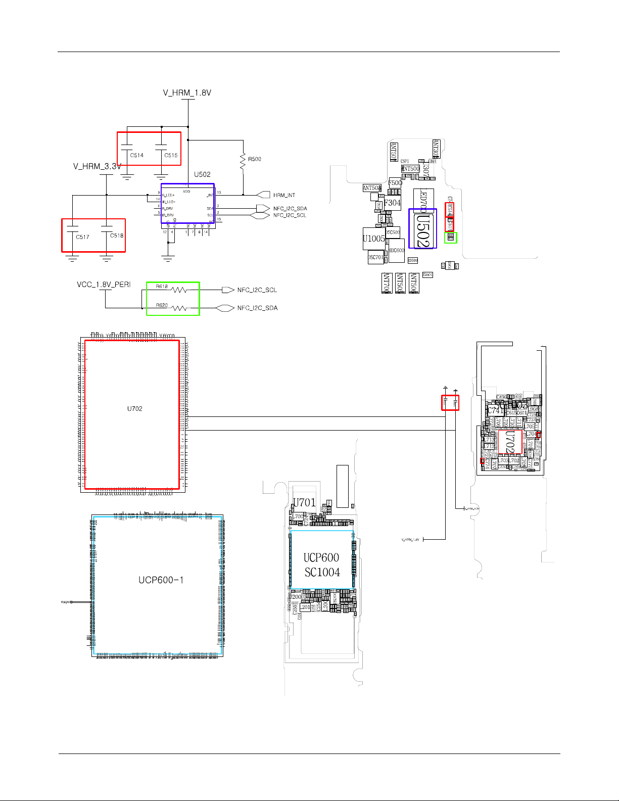
8-3-7-1.
HRM Sensor
HRM Sensor does not work
Check the voltage
C514, C515, C753
C517, C518, C796
Check R618, R620
(
Yes
Yes
I2C is OK?)
(
Yes
Replace U 502
HRM Sensor)
=1.8V
=3.3V
No
No
Replace U702, C514, C515, C753
Replace U702, C517, C518, C796
Replace UCP600
END
8-24
Confidential and proprietary-the contents in this service guide subject to change without prior notice.
Distribution, transmission, or infringement of any content or data from this document without Samsung’swritten authorization is strictly prohibited.
Level3Repair
8-25
Confidential and proprietary-the contents in this service guide subject to change without prior notice.
Distribution, transmission, or infringement of any content or data from this document without Samsung’swritten authorization is strictly prohibited.
Level3Repair
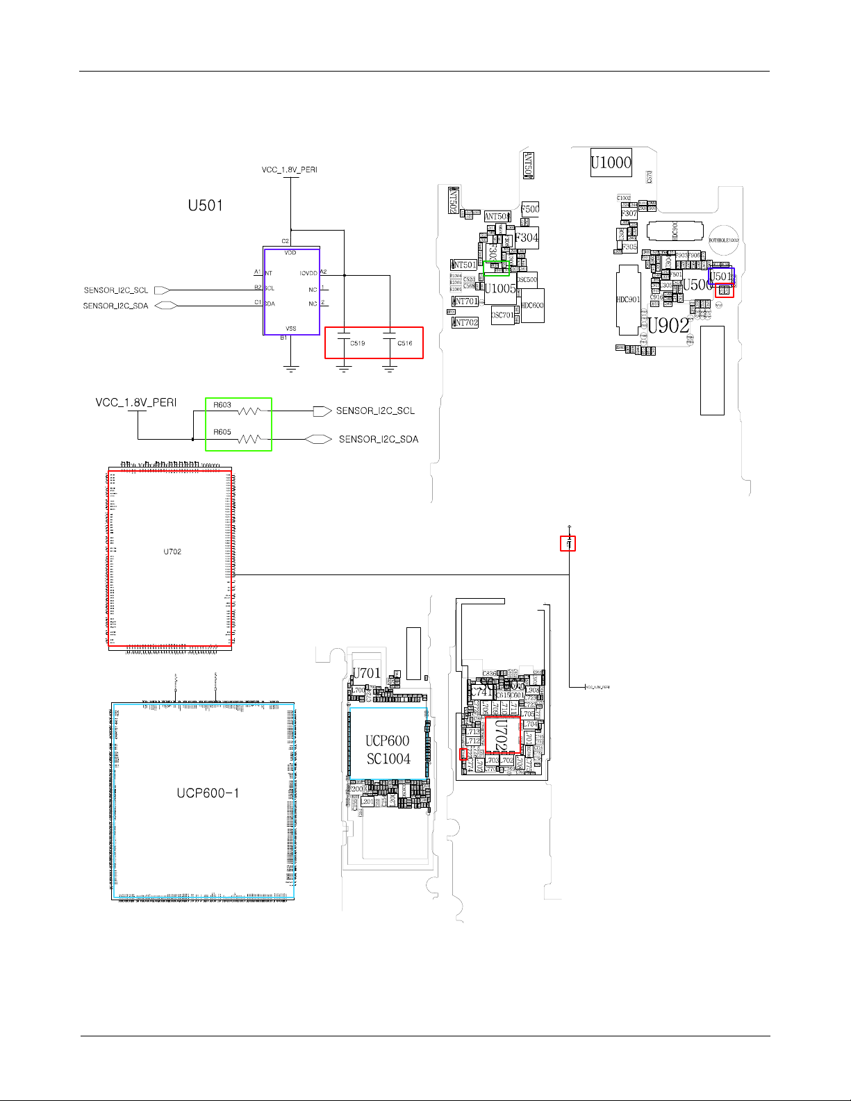
8-3-7-2.
Magnetic Sensor
Magnetic Sensor does not work
Check the voltage
C519, C516, C479
Check R603, R605
I2C is OK?)
(
Replace U 501
Magnetic Sensor)
(
Yes
Yes
Yes
=1.8
V,
No
No
Replace U702, C519, C516, C479
Replace UCP600
END
8-26
Confidential and proprietary-the contents in this service guide subject to change without prior notice.
Distribution, transmission, or infringement of any content or data from this document without Samsung’swritten authorization is strictly prohibited.
Level3Repair
8-27
Confidential and proprietary-the contents in this service guide subject to change without prior notice.
Distribution, transmission, or infringement of any content or data from this document without Samsung’swritten authorization is strictly prohibited.

Level3Repair
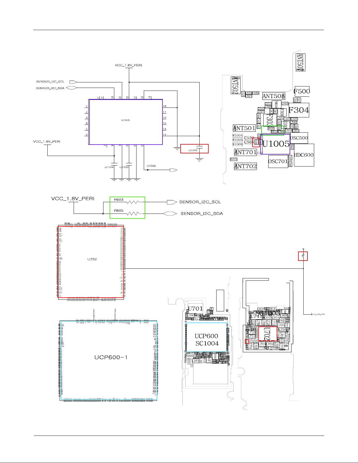
8-3-7-3. 6
Axis Sensor
Axis Sensor does not work
6
Check the voltage
C1002, C749
Check R603, R605
Replace U1005
(6
Yes
Yes
I2C is OK?)
(
Yes
Axis Sensor)
=1.8
V,
No
No
Replace U702, C1002, C749
Replace UCP600
END
8-28
Confidential and proprietary-the contents in this service guide subject to change without prior notice.
Distribution, transmission, or infringement of any content or data from this document without Samsung’swritten authorization is strictly prohibited.
Level3Repair
8-29
Confidential and proprietary-the contents in this service guide subject to change without prior notice.
Distribution, transmission, or infringement of any content or data from this document without Samsung’swritten authorization is strictly prohibited.

Level3Repair
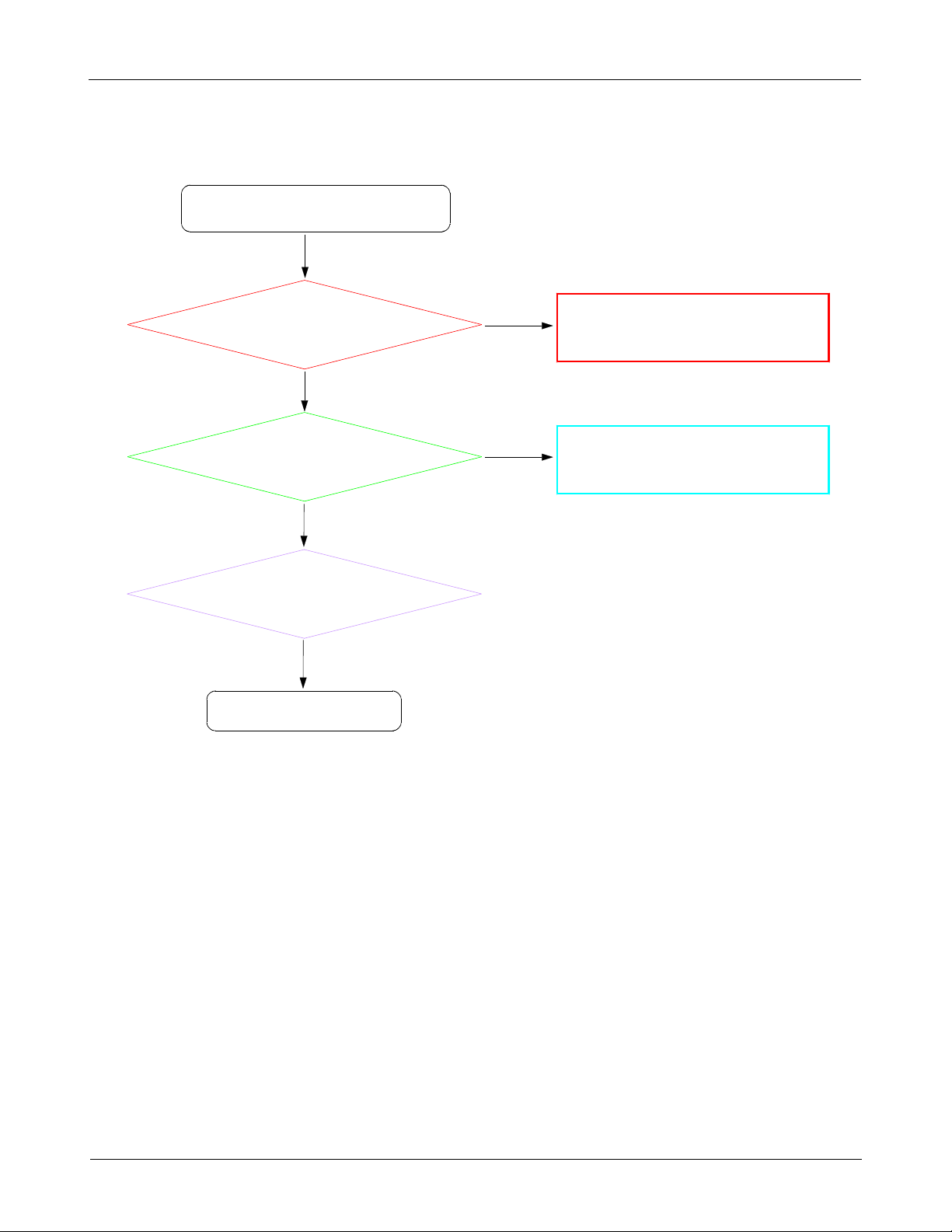
8-3-7-4.
Proximity Sensor
Proximity Sensor does not work
Check the voltage
C1001, C1002, C1003, C748=
3.3
Check R607, R609
I2C is OK?)
(
Replace U1000
Proximity Sensor)
(
Yes
V,
Yes
Yes
No
No
Replace U702,
Replace UCP600, ZD1000, ZD1001
C1001, C1002, C1003, C748
END
8-30
Confidential and proprietary-the contents in this service guide subject to change without prior notice.
Distribution, transmission, or infringement of any content or data from this document without Samsung’swritten authorization is strictly prohibited.
 Loading...