

Samsung SM-A730F Service Manual - Tshoo-7
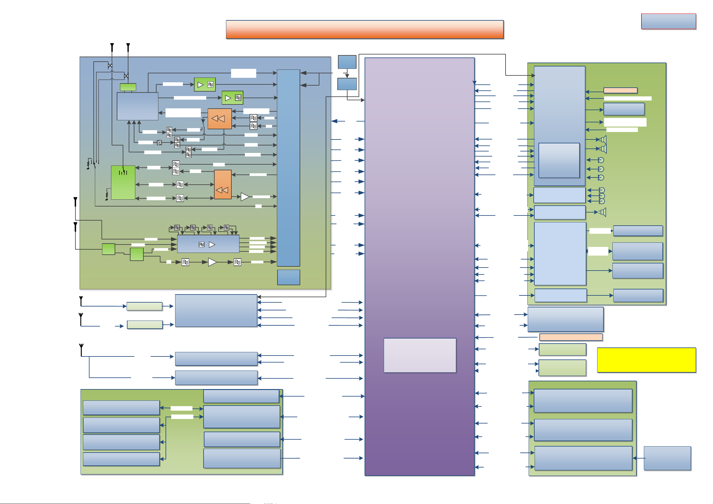
RF PART
TRANCEIVER
S937
(U2003)
FEMid
(U1001)
MMMB
(PAM1 001)
B7 DPX
(F1004 )
HB
PAM+SW
(PAM1 000)
2G Quad Tx
3G B1/2/5/8 Tx
LTE B1/2/3/5/8/12(17 )/20 Tx
LTE B7 Tx
LTE B7 TRx
DRX_TR_IN _B1_4
2G Quad Rx
3G B2/5
LTE B2/3/5/12/20 Rx
LTE B7 Rx
B40 T RX SA W
(F1003 )
LTE B40 TRx
Lower ANT1
(PRX_LMB)
HB
SP4T
(U1003)
Diversity LNA Module
(U7017)
DRX_TR_IN _HB
DRX_TR_IN _MB
TX_B7_38_40_41
2G Qua d,
B1/2/3 /4/5/8/20/28/66 Tx
B28 DPX
(F1006 )
LTE B28 TRx
LTE B28 Rx
LTE B28 Tx
DRX_AN T_MB
GPS
TCXO
(TCX2000)
26MHz
B38/41
TRX SAW
(F1002 )
LTE B38/41 TRx
DRX_AN T_LB
GNSS_ RF_IN
2G EGSM/3G B8/LTE B8 Rx
GPS SA W
(U3006 )
GPS LN A
(U3005)
MB
LB
3G B1/LTE B1 Rx
GPS
Extractor
(F2001)
LC
Notch
DRX_TR_IN _LB
DRX_AN T_HB
APT
Modulator
(U1017)
LTE B38/41/40 Rx
B38/41/40
LNA
(U1002)
Upper ANT
(DRX_LB)
Lower ANT2
(PRX_HB)
Diplexer
(F2000 )
B38/41 Rx
(F2003)
B40 Rx
(F2004)
B28 Rx
(F2005 )
B2/6 6 Rx
(F2002 )
B1 SLM
(U1000 )
B8 SLM
(U1010 )
B13 Tx
B12(17) Tx
LTE B13 Tx
LTE B13 TRx
LTE B4/66 Tx
LTE B13 Rx
LTE B4/66 Rx
LTE B4/66 TRx
LC
Notch
B13 DPX
(F1007 )
B4/6 6 DPX
(F1008 )
Upper ANT
(DRX_MHB/GPS)
SPDT
(U1016 )
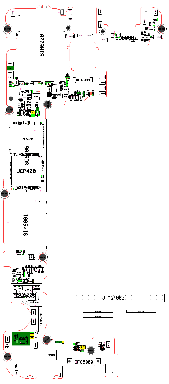
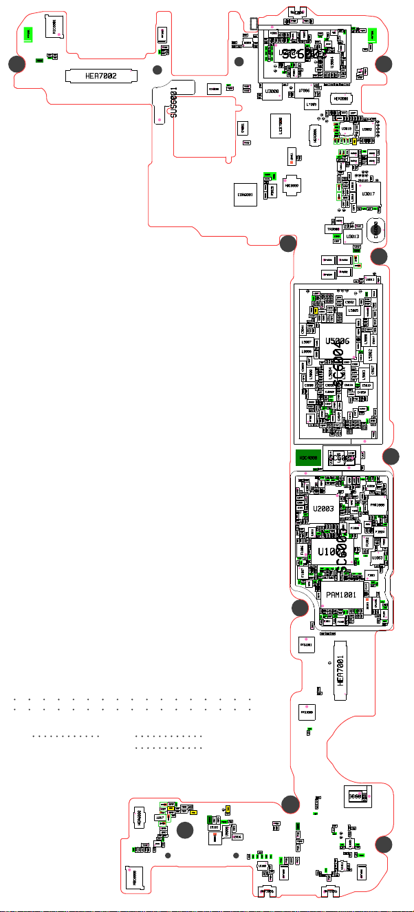
SM-A730F/DS Block Diagram
SENSOR PART
POWER PART
Audio Part
DISPLAY PART
AP
Exynos7885
(Lassen)
2.2GHz Dual + 1.6G Hexa
GPU G71 MP2 1.2G
(S.LSI)
POWER KEY
ACCEL & GYRO
LSM6DSL(STM)
T_FLASH_DATA(4)/CLK/CMD
Confidential
6.0" FHD+ OCTA (S.LSI S6E3FA7)
+ Touch IC (S.LSI S6Y661)
(SDC)
MIPI_LCD_D(4)_P/N
/ MIPI_LC D_CLK_P/N
LCD_RST/ OCTA_ID
VOLUME KEY
4GB LPDDR4
1866MHz
K4FBE3D4HM(SEC)
PMIC
S2MPU08
SPEEDY_PMIC
PROXIMITY + LIGHT + SVC LED
TMD37253S(AMS)
HALL IC x 2EA
S-5712C
(SEIKO)
PMIC_AP32K
PMIC_CLK_32K
(To WAKEUP IC/Sensor Hub)
PMIC_TCXO_IN_26M
IFPMIC_JIGONB_N From IFPMIC
PWR_EN
PMIC_WRSTBI
SOC_PSHOLD
TSP_I2C_SDA/SCL / TSP_INT
MIF_PWR_EN
/ G3D_PWR_EN
/ CP_PWER_UP
/BOOT_LDO
VOL_UP/DN
PMIC_IRQB_N
PMIC_TCXO_EN
SIM1_DATA/RST/CLK
NFC_SWP
9 BUCK, 37 LDO
USB 2.0 C Type
KQ 31MW1-24P(HRSK)
MUIC_D_P/N
/ MUIC_ID
FLASH LED
RM435GA (SBS)
IF_PMIC_INTB
/ IF_PMIC_I2C_SCL/SDA
FG_ALRTB_N /
FG_I2C_SCL/SDA
CAM_FLASH_EN
EMMC_D(8)
EMMC_CLK/CMD
/ EMMC5.0_RCLK
MAIN MIC
EAR_SPK
RCV (AAC)
PM_I2S0
Audio
CODEC
16M+8M FF CAM(SR846+S5K3P8SP)
(CAMSYS)
16M AF CAM (S.LSI 2P6)
(SEMCO)
MIPI_FCAM1_D(4)_P/N
MIPI_FCAM2_D(4)_P/N
FCAM_I2C_SDA/SCL
FCAM_EEP_I2C_SDA/SCL
/ FCAM_RST_N / FCAM_MCLK
MIPI_RCAM_D(4)_P/N
MIPI_RCAM_CLK_P/N
RCAM_I2C_SDA/SCL
RCAM_AF_EEP_I2C_SDA/SCL
/ RCAM_RST / RCAM_MCLK
HALL_INT/ COVER INT
OCTA DCDC
SM 3004B(SM)
SHUB_SPI/ MCU_AP_INT/
AP_MCU_INT/ MCU_RST
32GB eMMC 5.1
KLMBG2JETD-B041(SEC)
SIM1
GRIP_I2C_SDA/SCL
GRIP_INT
SPK AMP
TFA9872CUK(NXP)
SPK
SUB MIC
Flash Driver IC
KTD2692(KINETIC)
VOICE_ SPI/INT/RST/DATA
USB_AP_D_P/N
AP _UART_RXD/TXD
PRESSURE
LPS22HB(STM)
GRIP
A96T326(ABOV)
SENSOR HUB
STM32F410(STM)
FINGER PRINT SENSOR
ET510C(EGIS)
BTP_SPI/ BTP_CHECK
BTP_RST_N/ BTP_IRQ
SENSOR_I2C_2
SIM2_DATA/RST/CLK
MAGNETIC
AK 09918C(AKM)
BATTERY 3500mAh
(SDI)
SENSOR_I2C_1
BT / WIFI
(ANTENNA)
DIPLEXER
BT/WIFI/FM
S5N5C12X01-6630(S.LSI)
WLAN_SPDY_FROM/TO_S612
EARJACK
(ANTENNA)
WLAN_RX/TX_IQ
NFC
SEN81RRX(S.LSI)
NFC+MST
(ANTENNA)
NFC_ANT
NFC_I2C_SCL/SDA
NFC_SPI/ NFC_EN/ NFC_IRQ
MST
ISP7022(IMAGIS)
AOUT/BOUT
MST_DATA_A/B
RFIC_SPEEDY
RFIC_RESET
PRX1 I/Q
TX0 I/Q
PRX0 I/Q
DRX0 I/Q
DRX1 I/Q
SIM2/ uSD card
WAKEUP IC
DBMD4HD171(DSPG)
SPK_AMP_I2C_SCL/SDA
WB LINEAR 10Pi
MOTOR (MPLUS)
MAIN MIC
EAR MIC
SUB MIC
BT_SPDY_FROM/TO_S612
FM_SPDY_TO_S612
CP_UART_RXD/TXD
SPK_I2S3
PMIC_ONOB
PMIC_IRQBC
SOC_RESET_N
SOC_WRESET_N
LNA
FM_ANT
PRX2 I/Q
DRX2 I/Q
GNSS_BBI/Q
GNSS_SPEEDY
EAR MIC
Diplexer
(F1000 )
CLK
Buffer
(U2002)
TCXO_ IN
G_T CXO_IN
PDET
Coupler
Coupler
SP 4T
(U1008 )
B12 T X SAW
(F1011 )
B13 T X SAW
(F1010 )
IF PMIC
(Charger/FG/OTG/M
otor)
S2MU004(S.LSI)
Motor P/N
SIM2 part is blocked in SM-A730F
(Single SIM model)
BH6009
BH6007
ANT5001
ANT5007
ANT5005
ANT5006
ANT3000
VR6000
C6057
VR6001
C5111C5112
R5004
R5022R5023R5024
ZD5012ZD5013
R6004
ZD6002
ZD6017
C6017
R5026
ZD5014
C5114
R5031
C5149
C5150
C5043
L5017
C5023
C5011
C5059
C5057
C5037
C5077
C5099
C5098
C5012
C5002
R5051
Q5000
R5001
R5002
R5003
R4017
R4020
R4016
R4019
C5058
C5060
TP4007
TP4008
UME5000
TP4000
TP4004
C4043
C4082
R7000
C4075
C4083
C7007
C4078
SC6006
TP4005
TP4001
XCP_GPIO4000
TP_XCP_RF_ON4000
UCP400
XCP_GPIO4001
C4003
C4012
C4047
C4080
C4016
C4077
ZD6009
C6014
C6013
R6036
C6015
C6016
R6003
R5032
C5028
ZD5000
C5033
C5036
C5064
C5158
L5009
C5016
R5016
R5007
U5001
ZD5002
ZD5007
R5012
C5097
C5100
SC6001
TH5001
R5020
R5029
D5000
R5006
R5010
TP5000
R5009
R5011
R5015
C5004
R5008
TP5003
C5087
R4048
C5089
C5090
L7001
TP4006
C6010
R4015
R4049
L7000
C7015
TH4000
R4014
C6009
C7009
C4005
R4011
GNSS_ADC_VIN_I
R4006
R4007
R4010
R4012
C4081
TP_XGNSS_GPLL_ANA_EXT
GNSS_ADC_VIN_Q
C4032
C4028
C4026
SIM6000
D6001
L6020
C6012
D6000
D6002
D6003
D6004
ZD6003
C6031
C6029
C6023
L6005
C6024
C6025
C6030
C5009
VR6015
C5147
C5154
C5105
BH6008
R4022
R4026
C5088
R4046
R4047
C5084
R4018
R4021
TP5002
TP5012
TP5005
TP5006
TP5007
C5125
R5013 R5014
TP_EMMC4000
C5093
TP5008
TP5001
TP5014
L6003
L6002
R6002
R5050
C4079
C5124
C5142
R5018
TP5010
TP5011
TP5004
C4084
R4002
R4040
C4076
R4025
R4029
TP_XRTC_XTO
TP_SPEEDY
R4013
C4027
C4029
U6002
ANT2002
VR2000
BH6000
ANT6001
ANT1010
VR6003
L6000
L6001
C6000
C6007
ZD6000ZD6001
ZD7009
C7006
HEA7000
ZD7008
R4034
VR6002
ZD7007
R4037
ZD7005
R4031
C6027
ZD7006
R4030
R6012
C6026
C7032
U7008
R4038
R4041
C7033 C7034
C7000
C7002
C7004
U7007
C7005
C7031
TP6005
TP6003 TP6004
TP6006
C7030
U7005
C7025
C7003
C7016
C7020
C7018
C7024
C7027
C7026
U7003
U7001
U7002
U7004
C7017
C7019
C7023
C7021
ANT2005
ANT1014
BH6002
VR1013
C7001
ANT1004
ZD7010
VR6009
L7004
C7010
ZD7000ZD7001
VR1010
C7011
R4042
SC6009
C7014
R4024
R4028
R4039
C7012
ZD7002
ZD7003
ZD7004
L7003
C7008
C7013
ANT6000
ANT2004
L2001
VR2001
L2009
ANT1012
L2004
VR1011
L2010
C2005
L2017
L2018
BH6010
F2000
L2011
L3010
C3048
L3007
L2003
C3042
L2005
L3018
C3043
L2007
ANT1013
U3005
F2001
L2006
VR1012
L2015
L3008
C3053
C3045
C3050
ANT5000
ANT5004
ANT6002
R5049
L7002
R5027
ZD6005
C5113
L6004
ZD6004
ANT6003
C6022
L6006
ZD5001
C6028
ZD6007
ZD6006
C7022
BH6004
ANT1007
VR1004
VR6011
SIM6001
C6033
R6013
C6032
R6014
C6034
VR6004
C6056
ZD6008
R6011
TP_VOICE_TXD
TP6001
R6010
C6005
R6001
R6006
C6001
C6020
U6001
U6000
C6021
C6008
C6018 C6019
C6003
C6006
C6004
TP6000
C6002
C7046
TP6008
C7064
R4023
R4027
R7008
R7009
TP6002
TP6009
TP6007
C7072
C7074
C7062
C7063
C7065
C7075
L7013
C7061
F7013
C7230
F7012
U7016
F7010
F7014
L7014
L7009
SC6000
C7052
F7011
TP_DSDA
R1007
TP1000
C1077
U1011
U1007
SC6007
C1065
C1076
C1061
VR1007
ANT1005
VR6005
TP_HALL_INT
C3056
BH6006
U3007
L3011
L3012
C7040
C7042
C7044
C6036
C7043
C7041
U7009
U6003
U7010
U7011
U7012
U7013
C7035
C7036
C7038
C7037
C7039
C6035
C7076
C7070
C7069
R7010
ZD7011
C7231
C7071
C7067
L7012
L7011
L7010
C7053
C7057
C7056
C7058
ANT5002ANT5003
JTAG4003
JTAG4001JTAG4002
JTAG4000
SUS6000
TP1001
TP1002
TP1005
C5000
C5120
TP1004
R5041
VR1014
R5042
C1070C1075
BH6005
R1013
ANT1015
CON6002
R6026
R6027
R6028
R6030
R6025
C5127
ZD5010
R5039
R5040
C5034
C5126
ZD5004 ZD5005
ZD5003
ZD5006
ZD6010
L6013
L6015
ZD6011
ANT1009
L6012
VR6008
BH6001
R6031 R6033
VR1008
C6048
ZD6013
R5037
R5038
ZD5008
ZD5009
IFC5000
ANT3006
VR3002
VR3003
C3098
L3017
MIC6001
ANT2001
C6041
R6018
C6042
R6021
VR6019
ANT2003
VR2002
C2012
L2016
C2015
L2014
HEA7002
L2013
C2000
U2001
L2002
L2012
C6055
VR6007
VR6006
CON6000
VR1009
F2005
C2011
C2017
L2040
L2042
C2020
C2014
C2062
C2010
C2016
C2018
C2019
L2008
C2008
C2009
SC6003
C2004
C2006
C2007
C3061
U3008
R3002
R3007
C2061
L2039
L2041
C2051 C2052
U2004
TP2000
C2023
C2024
TP2001
L2024
C3099
L2033
L2037
L2038
F2003
F2004
C2053
C2059
L2036
C2058
C2060
C2054
L2034
C2074
C2073
C2071
C2069
C2067
C2068
L2030
C2034
C2031
C2033
C2032
C2041
L2027
L2026
F2002
C3062
TP3009
U7006
C7029
C7054
L7005
SUS6001
CN6001
LED7000
HEA3001
R5005
R5034
ZD5011
C5021
HDC5000
R5025
TP5009
C5062
C5130
C5072
C5005
C5133
C5134
C5044
L5007
L5006
C5007
C5039
L5000
C5076
C5008
C4013
C5085
C5157
C5051
C5052
C5078
TR7000
HDC4000
L2046
C2013
C2003
U2002
L2020
R2000
C2045
C2044
L2019
C2025
C2021
C2026
U2003
C2022
C1101
C1125
L2044
C1100
C2037
C2029
C2028
L2021
L1077
L1074
C1069
C1072
U1010
C1035
L1072
C1067
L1040
C1068
C1071
C1038
L1088
C1013
C1012
F1006
U1001
L1078
L1075
C1165
C1073
L1121
C1164
L1068
C1006
C1066
L1071
F1007
C1168
L1122
C1167
C1166
U1016
CON6001
VR6018
C5092
C5116
C5118
R5028
R5033
F3001
C3040
C3035
C3041
C3039
C3016
U3003
C3022
C3036
L3000
L3006
C3028
L3005
C2072
C3007
C2070
C3006
C3018
WL_FEMCTRL_3000
C3019
R3003
U3004
C3020
C3017
TH4001
R4004
C3032
C3005
C3014
C3015
C3044
R3006
R3019
R7001
R7002
C7028
C7051
HEA3000
C3054
C3055
R3020
R3018
TP3014
TP3018
TP3017
TP3016
Q3000
R3022
TP3015
ZD3002
C3026
ZD3003
C3085
R3023
ZD3007
U3012
C3065
TA3000
C3031
C3057
ANT3005
ANT3004
L6007
R6016
R6015
L6010
C6040
C6046
R6024
C5006
C6037
R6017
C5091
L6008
C6038
C6039
C6043
R6020
R6022
C5055
L6009
C5048
R5048
R5000
C5024
C5045
C5040
C5020
C5025
C5143
C5144
C5146
C5003
C5061
C5135
U5006
C5041
C5017
C5035
C5029
C5137
C5001
C5136
C5138
C5066
C5081
C4088
C5129
C5079
C4041
L5004
C4042
C4040
C4044
C4048
C4000
C5030
SC6004
C4045
C5065
C4025
C4023
C4046
C4017
C4069
C5067
C4070
C4057
C4101
C4085
C4015
C4086
C4102
C4103
C4060
C4089
C4056
C4062
C4053
C4065
C5053
C4063
C4064
C4052
C4061
R4008
C4051
C4049
C4050
C4002
C4091
C4092
C4037
R7003R7007
C4034
C5049
C4004
C4033
C4031
C4011
C4001
C4014
C4036
C4007
C4030
C1170
SC6008
L1125
L1123
C4100
C1171
C2040
C2056
C3046
C3051
C2055
C2046
C2057
L2029
L2035
L2032
U3006
L2025
C3052
C2042
C2065
L3009
C2043
C1017
C1010
C1015
C1029
C1078
R2001
L1030
C1032
C1026
L1013
L1082
L1001
L1034
L1029
L1011
L1018
L1026
L1031
L1010
L1117
C1149
C1159
C1163
L1116
L1009
L1118
SC6005
C1099
L1110
L1120
L1115
C1158
L1114
C1157
C1162
L1126
C1148
C1156
C1161
C1160
L1119
C1138
C1139
C1140
PAM1001
C1102
C1124
C1126
C1103
C1127
L1100L1101
C1123
C1130
L1105
C1129
L1102
F1011
F1010
L1104
VR6013
C1121
L1014
L1019
C3030
VR3000
C3025
C3029
C3024
C3033
ANT3001
L3001
L3003
VR3001
C3034
F3000
L3002
L3004
C3027
C3001
C3000
U3009
C3002
VR6016
C3004
C3003
C3059
R3001
R3016
C3049
C3047
R3017
C3008
TP3000
R3010
R3011
R3012
R3013
R3014
R3015
R3005
C3010
TP3001
C3060
TP3007
TP3005
C3021
U3010
U3002
TP3003
TP3006
TP3004
TP3002
TP3008
C3092
C3091
C3009
C3011
C3023
R3000
R3004
ZD3006
ZD3009
ZD3008
R3024
R3008
C3013
C3038
C3012
ZD3004
ZD3005
U3001
U3000
C3037
C3089C3090
C3071
C3074
C3087C3088
C3072
U3014
U3015
C3077
C3080
C3073
R4032
R4035
U3016
TP_NFC_IRQ
TP_NFC_EN
C3083
TP_NFC_CLK_REQ
TP_NFC_TCK
TP3010 TP3011
C3081
R3025
C3079
TP_NFC_CLK_3000
TP_NFC_SWDIO
TP_NFC_FIRM
TP3012
C3082
C3086
C3084
L3015
ZD3010ZD3011
C3093
C3094
U3017
C3096
L3016
C3095
C3097
C3070
C3068 C3069
C3076
C3075
Debug_TP
TP3013
C3078
MST_DATA_B_TP
MST_DATA_A_TP
VR6017
C3058
C3066
U3013
CN6000
C3064
C3063
ANT3003
ZD3001
ZD3000
ANT3002
TP_COVER_INT
L3013
U3011
C3067
VR6014
L3014
TP5016TP5017TP5018
TP5013
TP5015
C5026
C5141
C5132
C5032
C5131
C5164
R5017
L5005
OSC5000
C5014
C5038
C5083
C7232
C5075
C5139
C5071
C5031
C5073
C5056
C5050
C5046
C5063
C5080
L5008
C5047
C5022
C5140
C5010
L5002
C5013
C5018
C5068
C5070
C5027
C5069
L5014
L5003
C4087
C4068
C5015
C5019
C4067
C4066
C4059
C4058
C4105
C4022
R4009
C4024
C4010
C4055
C4054
C4009
C4093
C5128
C4071
C5082
C4072
C5086
C4090
C4039
C4074
C4073
C4020
C5074
C4006
C4018
C4095
C4097 C4098
C4019
C4021
C4094
C4035
C4099
C4008
C4096
C4038
VR6010
C1169
L1124
U1017
C2001
C2063
C2027
C2050
L1087
C1021
R1002
R1003
R1004
L2028
L2031
C1080
C2036
L2022
C2030
C2035
L2000
U1008
L1052
C1048
C2039
C2038
C1079
C2049
C2047
C1002
C1001
C1136
C1135
L1083
C1004
R1010
C1054
C1045
L1000
C1025
R2002
C1043
C1041
L2023
C1030
C1031
C1042
U1002
L1037
PAM1000
C2048
C1037
L1038
C1044
C1063
C1033
F1005
L1064
C1064
L1035
L1065
C1059
C1060
L1053
L1079
L1043
L1045
L1046
L1076
C1074
L1007
L1062
L1081
C1049
C1057
L1054
L1066
U1006
C1055
F1008
U1000
L1063
L1067
C1058
F1004
L1006
L1069
L1070
L1073
L1059
L1061
L1060
F1003
F1002
L1055
C1053
L1017
L1025
L1044
C1047
L1024
L1050
L1047
U1003
C1023
L1056
C1019
C1039
R1016
C1050
L1057
C1152
C1151
L1051
C1145
C1147
C1155
L1112
F1001
L1111
L1113
L1108L1109
C1153
C1144
C1146
C1150
C1154
C1184
C1183
L1129
C1143
C1142
R1011
C1141
L1023
L1016
CPL1001
L1022
ZD1001
L1106
L1107
C1000
C1131C1132
C1137
L1015
R1012
C1027
C1028
L1020
TH2000
CPL1000
C1133
C1134
L1103
R2007
L1005
C2066
R1000
C1128
L1002
RFS1001
TP_OLED_RST
HEA7001
C1122
L1004
RFS1000
L1008
L1127
R6023
MIC6000
HEA6000
R6019
L2043
TCX2000
C1095
L6018
ZD6014
C6053
C6051
R6032
R6035
C6049
C6052
L6014
R6034
C6050
L6019
ZD6012
C6054
L6017
ZD6016
ZD6015
L6016
L6011
C6047
C7047
C7045
C7050
U7014
TH5000
C7048
C6044
C6045
C7049
R5019
R5021
TP_4000
R4043
R6029
R4044
R5035
C5123
C5119
C5117
R5030
C5101
U5000
D5001
VR6012
C1024
C5115
L5016
C1020
L1003
L1032
C1005
C1008
C1011
C1046
U1009
C1173
L1048
C1034
C1036
VR1003
ANT1003
C1174
L1093
L1094
ZD1000
C1022
VR1001
R1008
R1001
L1021
VR1005
VR1006
VR1015
C1009
L1012
ANT1008
ANT1001
C2064
SC6011
C2002
L1130
C1056
C1007
C1172
TP1003
C1181
C1062
TP1011
L1091
L1097
U1005
L1058
L1090
C1018
VR1002
L1039
C1082
C1097
C1016
C1014
U1012
L1027
C1176
L1041
L1028
C1003
C1084
ANT1006
VR1000
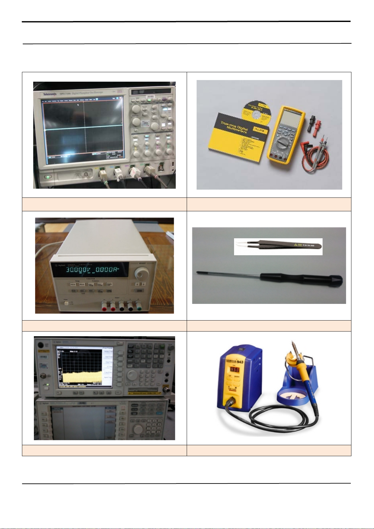
8. Level 3 Repair
Power Supply
+ driver, ESD Safe Tweezer
8960 & Spectrum Analyzer
Soldering iron
8-3. Flow chart of Troubleshooting.
Oscilloscope
Digital Multimeter
Confidential and pr oprietary-the contents in this service guide subjec t to change without prior noti ce
Distribution, transmission, or infringement of any content or dat a f rom this document without Samsung’s written authorization is strictly prohibited.

8. Level 3 Repair
Yes
No
Change the battery.
Yes
Yes
Sound or Vibration is ok?
Yes
No
No
Yes
No
Yes
Check the Clock TCX2000 & U2006
Is the frequency 26MHz?
No
Yes
Is it more than 3.8V?
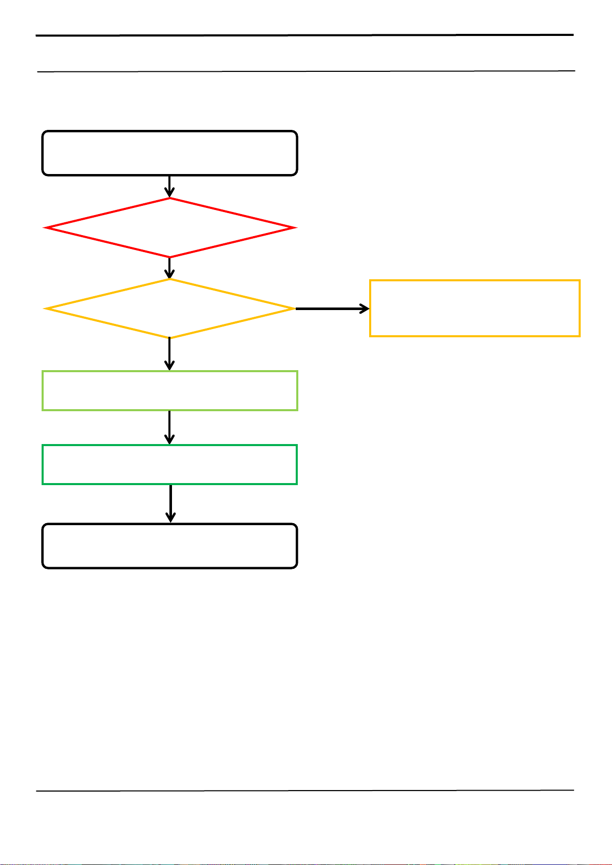
8-4-1. Power On
Mobile phone does not power on.
Check the Battery Voltage.
Power-on the phone and check
the power-on sound
or motor Vibration.
Charging the battery by TA.
If its voltage level is extremely low
(under 3.0V),
Change the FRONT-LCD ASSY
Check the voltage level at
R5002 while pressing power
key. Is the voltage high?
Check the signal of
SOC_PSHOLD = 1.8V
Check the initial operation
Replace the Power key FPCB
Check the output voltage of U5006
L5000 > 0.8V, L5014 > 0.8V, L5003 > 0.8V,
L5002 > 0.8V, L5004 > 0.8V, L5005 > 1.1V,
L5006 > 1.3V, L5007 > 2.0V, L5008 > 0.8V,
C5049 > 0.8V, C5050 > 1.8V, C5052 > 0.9V,
C5065 > 1.2V, C5066 > 1.8V, C5053 > 0.8V,
C5074 > 1.8V, C5082 > 1.2V,
If the output voltage is not normal, Change the
U5006.
※ Each voltage level has ±10% margin.
Replace the TCX2000 & U2003
※ Test condition (Oscilloscope setting)
: 20.0us.div (time division)
END
Confidential and pr oprietary-the contents in this service guide subjec t to change without prior noti ce
Distribution, transmission, or infringement of any content or dat a f rom this document without Samsung’s written authorization is strictly prohibited.
8. Level 3 Repair
Yes
Yes
Abnormal
Normal
Abnormal
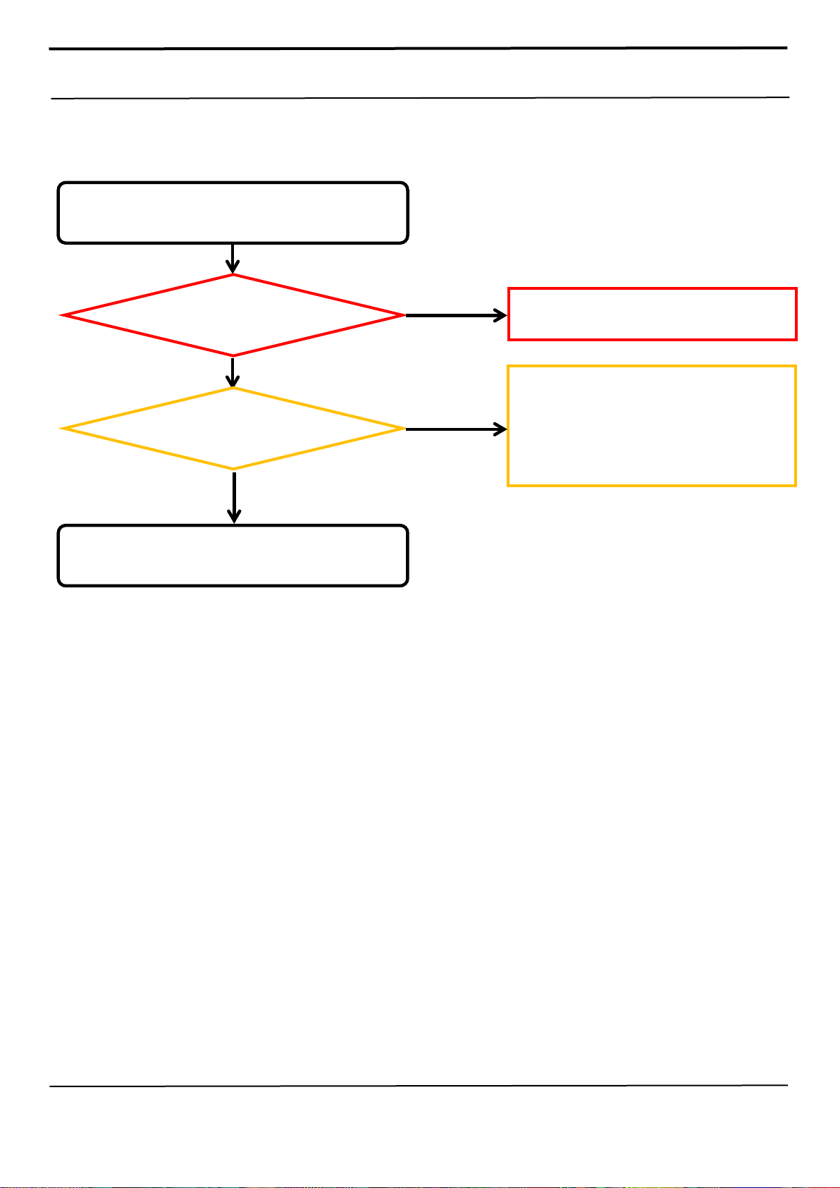
8-4-2. Initial
Re-download latest SW on the
Initial Failure
mobile phone
Re Check "Power on"
Trouble shooting process
Change U5006
Abnormal
Check the TCX2000 & U2003
(Crack, open etc.)
Check the U5006 (Crack etc)
Change PBA
END
Confidential and pr oprietary-the contents in this service guide subjec t to change without prior noti ce
Distribution, transmission, or infringement of any content or dat a f rom this document without Samsung’s written authorization is strictly prohibited.

8. Level 3 Repair
Yes
Yes
Yes
Yes
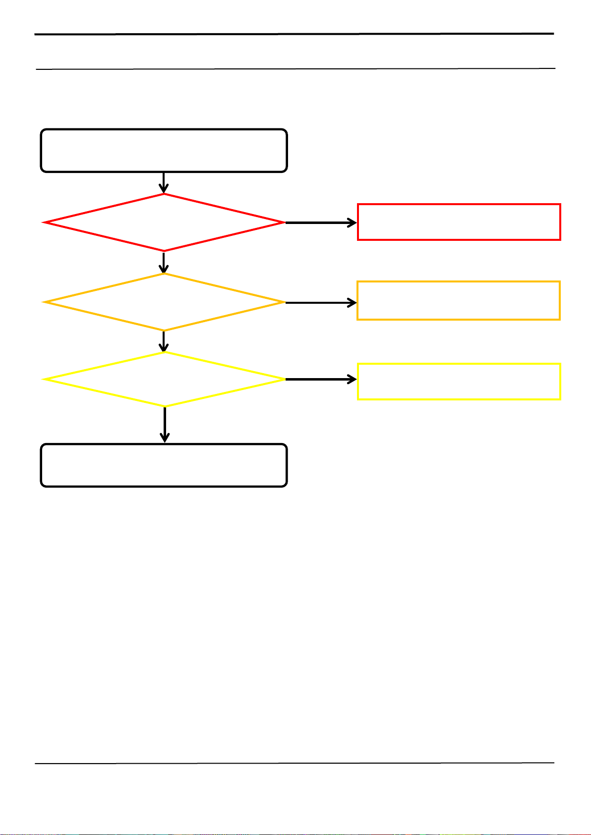
8-4-3. SIM Part
Is SIM1or2 socket ok?
Insert SIM card
No
Replace SIM1 or 2 socket
END
No
No
Change to the new SIM card.
If it doesn`t still work SIM card after
changing
the SIM card, Check the U5006
(Crack etc)
Check the UCP400 (Crack etc)
Check the SIM1 or 2 Voltage.
SIM1(C6033)or SIM2(C6015)
= 1.8V or 3.0?
Check the SIM
RST / IO / CLK.
SIM1 : (SIM6001’s C2, C7, C3)
SIM2 : (SIM6000’s C2B,C7B, C3B)
No signal
Confidential and pr oprietary-the contents in this service guide subjec t to change without prior noti ce
Distribution, transmission, or infringement of any content or dat a f rom this document without Samsung’s written authorization is strictly prohibited.
8. Level 3 Repair
Yes
Yes
Yes
Yes
8-4-4. T-Flash Part
Insert T-Flash card
Is SIM2 socket ok?
No
Replace SIM2 socket
END
No
Change to the new T Flash card.
If it doesn`t still work T Flash card after
changing
the T FLASH power, Check the U5006
(Crack etc)
Check the T-flash Voltage.
(C6014) = 3.0?
Confidential and pr oprietary-the contents in this service guide subjec t to change without prior noti ce
Distribution, transmission, or infringement of any content or dat a f rom this document without Samsung’s written authorization is strictly prohibited.
8. Level 3 Repair
Yes
Yes
Yes
Yes
8-4-5. Charging Part
Check the CHG_IN_5V(L5016) = 5V
Insert TA / USB
Charging Sequence Start
VBUS_IF_5P0(C5119) = 5V
Battery is Charging?
No
Replace IFC5000
No
No
Replace U5000
Replace U5001
END
Confidential and pr oprietary-the contents in this service guide subjec t to change without prior noti ce
Distribution, transmission, or infringement of any content or dat a f rom this document without Samsung’s written authorization is strictly prohibited.
 Loading...