

Samsung SGH-S7330, GT-S7330 Troubleshooting
10. Flow Chart of Troubleshooting
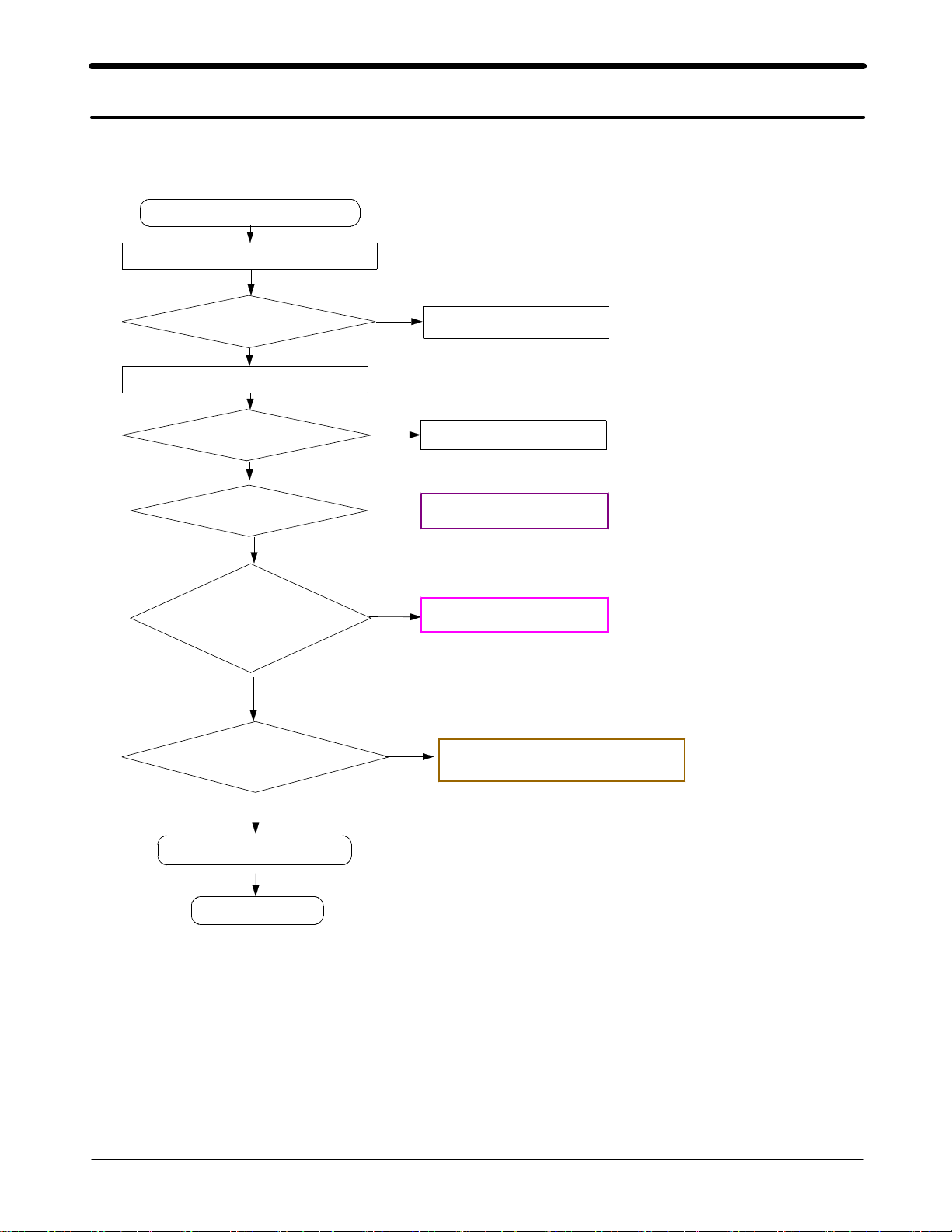
10-1-1.
Power ON
Power On' does not work
'
Check the current consumption
Yes
Current consumption
Check the Vbat Voltage
Voltage
#3
Pin
mA
>= 100
Yes
>=3.3V
Yes
of D400 is high?
Yes
No
No
Download again
Charge the Battery
No
Check D400
Check the PMIC output
voltage
C422,C424,C423,C417,
(
C428,C418)
Yes
Check Pin#3 of TCX200
is
MHz?
19.2
Yes
Check the initial operation
END
No
No
Check U400
Check the clock generation circuit
relatedtoTCX200
(
)
10-1
SAMSUNG Proprietary-Contents may change without notice
This Document can not be used without Samsung's authorization
Flow Chart of Troubleshooting
10-2
SAMSUNG Proprietary-Contents may change without notice
This Document can not be used without Samsung's authorization
V_RF_S2_2.1V
Flow Chart of Troubleshooting
< Power Management IC >
V_RF_S3_2.7V
A7
MPP1|AMUX_IN1
B7
MPP2|AMUX_IN2
K3
AMUX_OUT
L2
MPP3|KPD_DRV_N
L1
MPP4|LCD_DRV_N
L3
VIB_DRV_N
D7
MPP5|RUIM_M_RST
H7
MPP6|RUIM_RST
D6
MPP9|RUIM_M_CLK
H6
MPP10|RUIM_CLK
D5
MPP11|RUIM_M_IO
H5
MPP12|RUIM_IO
K2
MPP7|CBLPWR_N
B4
MPP8|REF_OUT
D4
OPT_1
H8
OPT_2
C11
REF_BYP
E10
REF_GND
D10
REF_ISET
B5
SPKR_IN_M
B6
SPKR_IN_P
A5
SPKR_OUT_M
A6
SPKR_OUT_P
D8
TCXO_EN_1
E4
TCXO_EN_2
E11
TCXO_IN
H10
TCXO_OUT_1
B10
TCXO_OUT_2
F11
TCXO_OUT_RF
G4
USB_DAT
J1
USB_D_M
J2
USB_D_P
H2
USB_ID
F4
USB_OE_N
F2
USB_OVP_G
H4
USB_SE0
H1
USB_VBUS
1
3
E
B
P
T
A
G
_
B
V
D
D
V
(0.5~2.0 vpp)
(L:~0.45V, H:2.15V~)
(L:~0.45V, H:2.45V~)
D
D
D
N
N
N
G
G
G
6
5
7
E
E
E
R400
VREG_SD_MEM_2.8V
VREG_SD_2.8V
L400
VBATT
R409
C438
VREG_MSMP_2.6V
TP_HSET_BIAS
ON_SW
PM_INT_N
PON_RESET_N
SLEEP_CLK
C439
C401
L401
R412
PMIC_SBDT
D400
3
1
POS
NEG
2
2
1
BAT400
OSC400
1
2
PS_HOLD
BOOT_SW
C415
C435
C419
R401
C436
C421
TA_VEXT_5V
R410
1
C400
0
1
1
9
2
4
1
5
7
1
1
1
L
L
F
B
B
A
G
K
H
A
3
F
V
V
C
R
N
M
IN
IM
2
5
5
R
K
A
S
M
A
_
_
S
U
_
L
P
S
M
_
G
R
M
D
S
_
M
D
_
_
D
_
_
D
D
D
D
V
D
D
D
V
D
D
D
V
D
V
V
V
V
U400
D
D
D
D
D
D
N
N
N
N
N
N
G
G
G
G
G
G
5
7
6
5
6
7
F
F
F
G
G
G
W
W
E
S
_
VREG_GP1
R
V
D
V
D
VREG_GP2
V
VREG_GP3
VREG_MMC
VREG_MSMA
VREG_MSME
VREG_MSMP
VREG_MSMC
VSW_MSMC
VREG_RFRX1
VREG_RFRX2
VREG_RFTX
VREG_RFUBM
VREG_RUIM
VREG_S2
VREG_S3
VSW_S2
VSW_S3
VREG_TCXO
VREG_USB
VREG_WLAN
ISNS_M
ISNS_P
XTAL_IN
XTAL_OUT
SBDT|SSBI
VCOIN
BAT_FET_N
CHG_CTL_N
HSET_BIAS
KPD_PWR_N
MSM_INT_N
PON_RESET_N
PS_HOLD
SLEEP_CLK
C
C
C
N
N
N
D
1
1
2
1
D
SBCK
SBST
VCHG
(1.5V~3.05V, Default 2.8V)
A3
A2
B1
L9
G11
K8
J11
K4
K5
A9
A10
A8
B8
L10
L8
L6
K7
K6
L402
A1
G2
B11
R432
D1
D2
R406
L11
K11
R407
F8
G8
E8
J10
E2
C2
C1
K1
L4
C10
G10
F10
K9
R413
TP_V_GP400
VREG_MSMP_2.6V
VREG_MSME_1.8V
VREG_MSMA_2.6V
C422C420
VREG_MSMC_1.2V
C424
C423 C430
C417
C425
VREG_USIM_3.0V
C427
C426
V_RF_S2_2.1V
1.25+0.1T
C428
C429
V_RF_S3_2.7VVREG_MSME_1.8V
1.25+0.1T
VREG_TCXO_2.8V
C418
C431
C432
VREG_BT_2.6V
C433
10-3
SAMSUNG Proprietary-Contents may change without notice
This Document can not be used without Samsung's authorization
Flow Chart of Troubleshooting
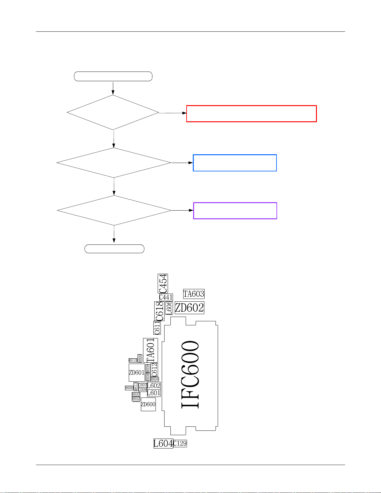
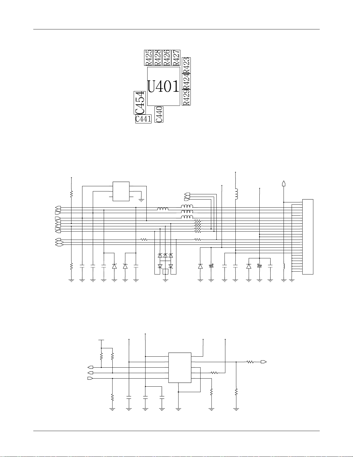
10-1-2.
Charging Part
Initial Failure
L606,C454
5.0V @
U401 pin5=High?
Check the Battery&TA
Yes
Yes
Yes
Yes
?
No
No
No
if it has some problem, it is to be replaced.)
(
Check the IFC600
Replace U401
Check the U400
END
10-4
SAMSUNG Proprietary-Contents may change without notice
This Document can not be used without Samsung's authorization
Flow Chart of Troubleshooting
VREG_MSMP_2.6V
R600
EARMIC_P
EARMIC_N
EAR_R
EAR_L
EAR_SW
JACK_INT
BOOT_SW
UART1_TX
UART1_RX
JIG_ON
USB_D_P
USB_D_M
R612
C607 C610
C608
< IF CONNECTOR >
T
N
L604
A
_
O
I
D
A
R
IFC600
1
1
2
2
3
3
4
4
5
5
6
6
7
7
8
8
9
9
10
10
11
11
12
12
13
13
14
14
15
15
16
16
17
17
18
18
19
19
20
20
21
NC
22
NC
23
NC
24
NC
25
NC
26
NC
27
NC
TA_VEXT_5V
ZD600
TA603
USB_VBUS_5V
C611 C618
6
0
6
L
ZD603
TA601
VBATT
C612
6
5
1
IO5
IO1
2
IO4
GND
34
IO2
IO3
R609
6
0
6
D
Z
C609
7
0
6
D
Z
L608
JIG_ON_TEST
UART1_RX_JTAG
UART1_TX_JTAG
L607
L601
L602
5
6
4
1
3
7
8
2
ZD601
R602
R603
R604
R606
R608
R610
ZD602
CHG_DETECT_N
CHG_INDICATE
CHG_EN_N
< CHARGER >
TA_VEXT_5V
C441
C454
ISL9214IRZ-T
CRDL
2
USB
3
_PPR
4
5
_EN
10-5
GND
11
U401
USB_VBUS_5VVBATT
101
BAT
9
ICDL
8
GND
7
USBON_CHG
6
IMIN
R426
R427
R423
R429
USB_VBUS_5V
R424
C440
VREG_MSMP_2.6V
SAMSUNG Proprietary-Contents may change without notice
This Document can not be used without Samsung's authorization
R425
CHG_CURRENT
R428

Flow Chart of Troubleshooting
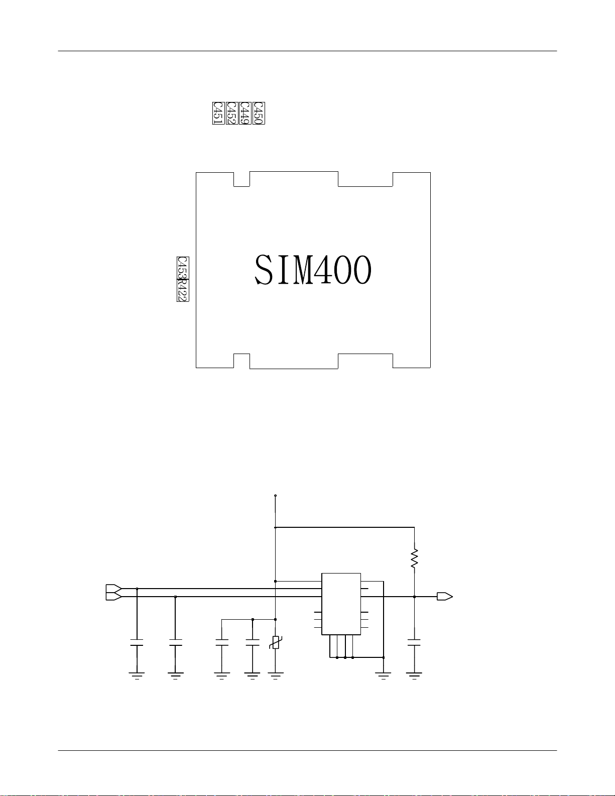
10-1-3.
Sim Part
Insert SIM is displayed on the LCD
"
Yes
Check the SIM connector's
SIM
(
Check the voltage at pin#1
pin#2,#3,#4 of SIM
connection to
400)
SIM card
Yes
of SIM
400 >= 3.0V ?
Yes
Is there any signals
400 ?
No
No
No
Resolder or change SIM
Check the U400
Check the U400
400
Yes
Check the SIM Card
END
10-6
SAMSUNG Proprietary-Contents may change without notice
This Document can not be used without Samsung's authorization
Flow Chart of Troubleshooting
SIM_RST
SIM_CLK
C449
C450
< U-SIM >
VREG_USIM_3.0V
SIM400
11
22
33
7
7
C451
C452
88
2
0
4
R
V
11 11
99
R422
6
6
5
5
4
4
1212
1010
13GG1415GG16
C453
SIM_IO
10-7
SAMSUNG Proprietary-Contents may change without notice
This Document can not be used without Samsung's authorization
Flow Chart of Troubleshooting
10-1-4.
Microphone Part
Microphone does not work
Is the assembled status of
microphone O.K?
Check the reference voltage on MAIN-MIC path
1.8V @
Is microphone ok?
END
Yes
Yes
Yes
R509
Yes
Yes
No
Replace the Front Assy'
?
No
No
Check the path
around MIC_BIAS circuit
Check UCP300
10-8
SAMSUNG Proprietary-Contents may change without notice
This Document can not be used without Samsung's authorization

Flow Chart of Troubleshooting
<KEY CONNECTOR>
KEY_LED_3.3V
HDC700
R703
R705
R707
R709
R711
R733
MIC1N_FMIC1P_F
KEYSENSE(0)
KEYSENSE(1)
4
1
7
R
V
C701
R732
C700
R702
R704
R706
R708
R710
R712
0
0
7
R
V
4
3
0
7
R
V
5
0
7
R
V
6
0
0
7
7
R
R
V
V
8
7
0
0
7
7
R
R
V
V
KYPD_MEMO
KYPD_11
KYPD_13 KEYSENSE(2)
KYPD_15 KEYSENSE(3)
KYPD_17 KEYSENSE(4)
KYPD_9
ON_SW
2
0
7
R
V
1
2
2
1
3
4
4
3
5
6
5
6
7
8
8
7
9
10
10
12
14
16
18
20
9
11
12
11
13
14
13
15
16
15
17
18
17
19
20
19
NC
NC
2122
1
0
7
R
V
10-9
SAMSUNG Proprietary-Contents may change without notice
This Document can not be used without Samsung's authorization

Flow Chart of Troubleshooting
<MAIN-MIC PATH>
MIC_BIAS
R509
MIC1_P
MIC1_N
C518
C521
C525
C520
C524
R510
C517
TA503
R513
C526
C523
R511
MIC1P_F
R512
MIC1N_F
10-10
SAMSUNG Proprietary-Contents may change without notice
This Document can not be used without Samsung's authorization
Flow Chart of Troubleshooting
10-1-5.
Receiver Part
There is no sound from the Receiver
Is the terminal of Receiver
Is there any signals at R723
Check HDC703
RECEIVER/SPEAKER/MOTOR FPCB.
O.K
?
and R724
#6, #8
END
Yes
Yes
Yes
?
No
Replace the Receiver
No
Check UCP300
Pin and
SPK_N_OUT
SPK_P_OUT
<SPK/RCV/MTR CONNECTOR>
VMOT_3.3V
HDC703
11
R722
3
7
C721
C720
9
1
7
R
V
TA700
1
7
R
V
C718
1
2
D701
10-11
SAMSUNG Proprietary-Contents may change without notice
This Document can not be used without Samsung's authorization
22
33 4 4
55 6 6
77 8 8
10
99
NC
NC
11
12
R724
10
C722
0
2
7
R
V
8
C719
1
7
R
V
R723R721
 Loading...