

Samsung SGH-M8800, GT-M8800 Troubleshooting

10. Flow Chart of Troubleshooting
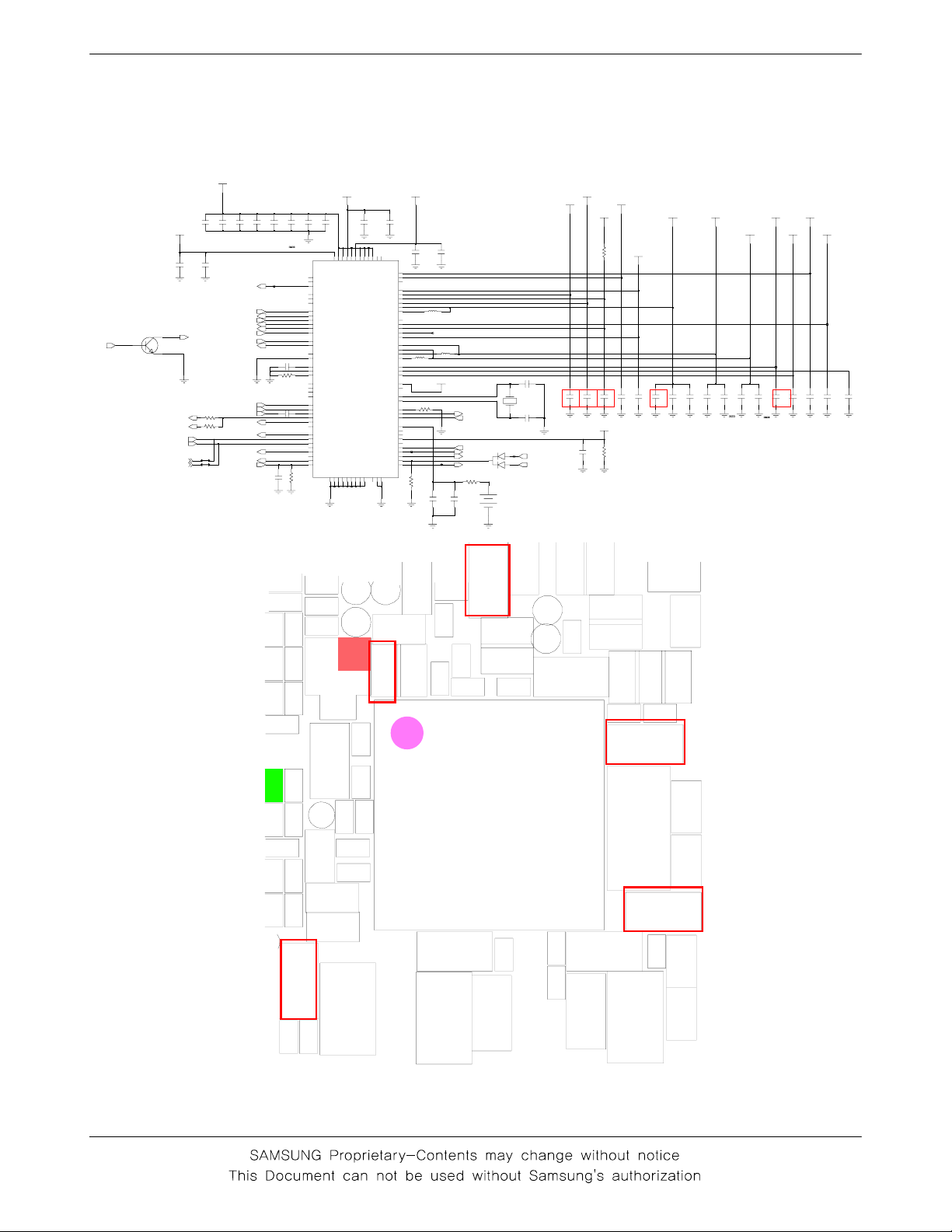
BASEBAND
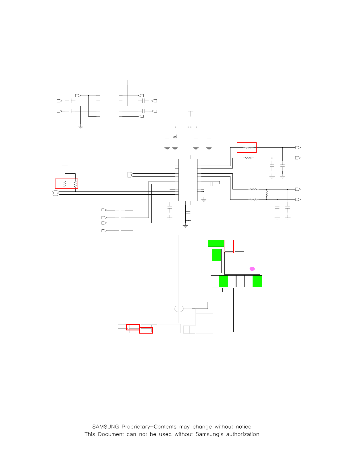
10-1
10-1-1.
Power ON
Power On' does not work
'
Check the current consumption
Yes
Current consumption
Check the Vbat Voltage
Voltage
F10(PS_HOLD)=2.6V
check the PMIC output
voltage(C414, C415,
C417, C418, C419
>= 100
>=3.3V
U402 PIN
mA
Yes
Yes
Yes
)
No
No
No
No
Download again
Charge the Battery
Check the PMIC related to
PS_HOLD
check the PMIC
Yes
check the TCX200
C201=
Check the initial operation
19.2
END
Mhz?
Yes
No
Check the clock generation circuit
relatedtoTCX200
(
)
10-1
Flow Chart of Troubleshooting
< JIG Detect >
JIG_ON
1
TR400
3
2
CLK19.2M_PM
USB_DM_MODEM
USB_DP_MODEM
USB_DM_JTAG
USB_DP_JTAG
TCXO_FF
C409
C452
JIG_ON_SW
VBATT_4.2V
0603
25V
C456
R402
R403
< Power Management IC >
0
1
K
6
G
S
C
4
0
2
7
L
MI
U
R
_
D
D
V
D
N
G
7
G
P
C405
1
4
1
A
A
3
R
2
K
S
P
_
S
D
_
D
D
V
D
V
VREG_RFUBM
PON_RESET_N
D
N
G
1
1
D
_
P
T
D
1
1
F
G
V
V
N
5
5
A
_
_
L
G
W
W
E
S
VREG_GP1
_
R
V
D
V
VREG_GP2
D
V
VREG_GP3
VREG_MMC
VREG_MSMA
VREG_MSME
VREG_MSMP
VREG_MSMC
VSW_MSMC
VREG_RFRX1
VREG_RFRX2
VREG_RFTX
VREG_RUIM
VREG_S2
VREG_S3
VSW_S2
VSW_S3
VREG_TCXO
VREG_USB
VREG_WLAN
ISNS_M
ISNS_P
XTAL_IN
XTAL_OUT
SBDT|SSBI
VCOIN
BAT_FET_N
CHG_CTL_N
VCHG
HSET_BIAS
KPD_PWR_N
MSM_INT_N
PS_HOLD
SLEEP_CLK
C
C
C
N
N
N
D
2
1
R
S
T
_
N
C429
C
4
1
5
V_RF_2.1V
C406
A3
A2
B1
L9
G11
K8
J11
K4
K5
A9
A10
A8
B8
L10
L8
L6
K7
K6
L402
A1
G2
B11
D1
D2
L11
K11
F8
SBCK
G8
E8
SBST
J10
E2
C2
C1
K1
L4
C10
G10
F10
K9
C
4
2
0
C400
10V
AMUX_OUT
JIG_ON_SW
BT_TCXO_EN
CLK19.2M_TCXO
0603
BT_TCXO_OUT
0603
USB_VBUS_5V
C401
SIM_RST
USIM_RST
SIM_CLK
USIM_CLK
SIM_IO
USIM_IO
REF_OUT
TCXO_EN
USB_DAT
USB_OE_N
USB_SEO
V_RF_2.7V
10V
C453
1005
C454
C404
C402
C403
TP_AMUX_OUT
C412
C431
C457
1005
C345
C341
C
3
3
1
C
3
5
0
C
3
5
5
C354
R
3
2
3
R
3
1
3
C300
C
3
5
7
C
3
3
7
T
U
_
O
X
U
M
_
A
10V
1
9
2
3
1
5
1
L
E
B
B
B
H
T
F
P
NI
C
M
A
R
G
S
M
A
_
_
B
S
M
M
D
V
D
_
M
_
D
D
D
_
D
V
V
A7
D
D
D
MPP1|AMUX_IN1
V
D
V
B7
K3
L3
L1
L2
D7
H7
D6
H6
D5
H5
K2
B4
D4
H8
C11
E10
D10
1005
R400
B5
B6
A5
A6
D8
E4
E11
H10
B10
F11
G4
J1
J2
H2
F4
F2
H4
H1
R408
0603
C
3
2
5
C
3
5
3
C
3
5
6
R
3
2
5
R
3
0
0
C
3
5
8
C
3
3
8
P
T
C
4
1
4
MPP2|AMUX_IN2
AMUX_OUT
MPP3|VIB_DRV_N
MPP4|LCD_DRV_N
KPD_DRV_N
MPP5|RUIM_M_RST
MPP6|RUIM_RST
MPP9|RUIM_M_CLK
MPP10|RUIM_CLK
MPP11|RUIM_M_IO
MPP12|RUIM_IO
MPP7|CBLPWR_N
MPP8|REF_OUT
OPT_1
OPT_2
REF_BYP
REF_GND
REF_ISET
SPKR_IN_M
SPKR_IN_P
SPKR_OUT_M
SPKR_OUT_P
TCXO_EN_1
TCXO_EN_2
TCXO_IN
TCXO_OUT_1
TCXO_OUT_2
TCXO_OUT_RF
USB_DAT
USB_D_M
USB_D_P
USB_ID
USB_OE_N
USB_OVP_G
USB_SE0
USB_VBUS
C305
C330
C324
C
4
3
3
TP_RESETOUT_N
C
4
1
6
C457
C454
V
U402
D
D
D
D
D
D
D
N
N
N
N
N
N
N
G
G
G
G
G
G
G
5
7
6
5
5
6
7
F
F
F
E
E
E
G
L
D
O
_
H
T
P
_
B
O
O
T
_
S
W
0
4
0
R
4
1
1
R
4
0
6
C
4
0
9
C401
R408
L
4
0
C
4
2
2
0
C
4
2
3
R401
0603
TP_PM_INT
3
0
6
0
R411
5
0
2
C407
L400
VBATT_4.2V
C453
L
4
0
2
C408
TP_RFUBM
L401
TP_SLEEP_CLK
R407
C437
R504
R
5
0
3
C
4
0
4
C
3
6
5
SSBI2_DATA
PMIC_SBST
ON_SW
PM_INT_N
RESET_N
SLEEP_CLK
C438
C452
1005
1
9
U
4
0
2
3
1
POS
NEG
2
R424
C408
C
4
2
6
C
4
2
7
1
2
OSC400
2
1
D400
BAT400
C407
C413
C432
TP_PS_HOLD
PS_HOLD
BOOT_SW
I
T
N
TP_RFUBM
V_MSMA_2.6V
_
M
_
P
P
T
C400
C
4
0
3
C
4
2
5
V_MSMP_2.6V
C417
C433
R
4
0
1
V_MSME_1.8V
VEXT_5V
C456
C
4
2
4
WPAM_BIAS_2.85V
R424
1005
C419
C420
3
0
6
0
R406
C319
C318
C
4
3
0
C412
L
4
0
1
V_USIM_3.0V
C421
R
4
0
0
C431
C417
O
S
C
4
0
0
C418
V_MSMC_1.2V
C414
C
4
0
5
V_RF_2.1V
C422
C424C418
C423
C
5
0
1
C
4
2
8
C
4
3
2
C
4
1
3
C
4
0
6
C
4
2
1
V_TCXO_2.85V
V_MMC_2.85V
V_BT_2.6V
C415
V_FEM_2.7V
C430
C429
C428
C416
V_RF_2.7VVBATT_4.2V
C425
C426
C427
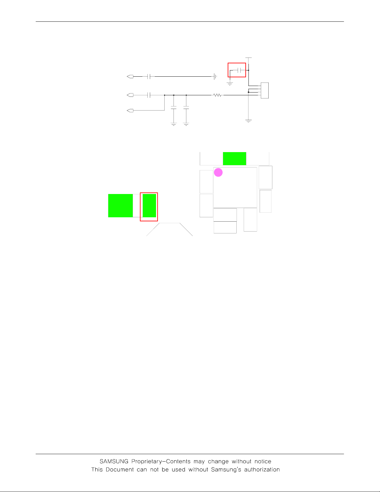
10-2
Flow Chart of Troubleshooting
10-1-2.
Sim Part
Insert SIM"is displayed on the LCD
"
Yes
Check the SIM connector's
SIM
(
pin#1(C442) of SIM
pin#2,#3,#4of SIM
connection to
400)
SIM card
Yes
Check the voltage at
3.0V ?
Is there any signals
400 >=
Yes
400 ?
No
No
No
Resolder or change SIM
Check the PMIC
Check the PMIC
400
Yes
Check the SIM Card
END
10-3

Flow Chart of Troubleshooting
< USIM Connector >
V_USIM_3.0V
USIM_RST
USIM_CLK
USIM_IO
C
4
4
3
C439
C443
SIM400
11
22
33 4
G
910
6
6
5
5
4
G78GG
R413
1005
4
3
6
C
4
4
2
1
5
2
C439
ZD401
C441
C442
R413
4
0
1
D
Z
C
4
4
1
SIM400
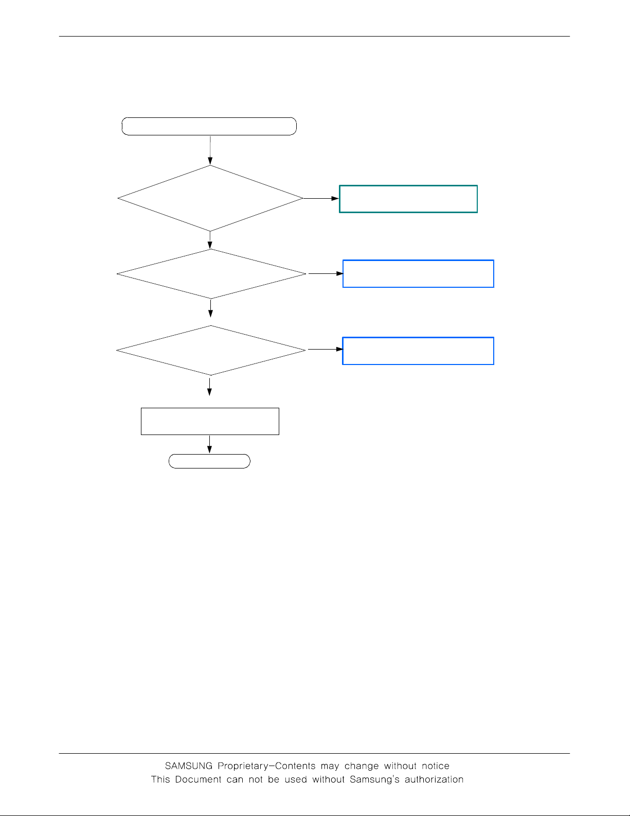
10-4
Flow Chart of Troubleshooting
10-1-3.
Charging Part
Abnormal charging part
C434 at USB_5V or
C435 at EXT_5V=5V?
When U401 is charging,
U401 pin
Check the battery&TA
Yes
Yes
#4 = "L"?
Yes
No
No
No
Resolder U402
Replace U401
Check the PMIC
END
Yes
10-5

Flow Chart of Troubleshooting
< Charging IC >
CHG_INDICATE
CHG_EN_N
R404
R409
R405
R410
C436
3
0
6
0
R423
VEXT_5V
USB_VBUS
3
0
6
0
C434
1
C435
1
2
3
4
5
0
CRDL
USB
_PPR
_CHG
_EN
GND
11
4
U401
USBON
BAT
ICDL
GND
IMIN
R409
U
VBATT_4.2VV_MSME_1.8V
10
9
8
7
6
5
0
0
1
R405
C436
R410
1005
1%
USB_VBUS_5V
0603
R404
C434
C435
10-6
Flow Chart of Troubleshooting
10-1-4.
Microphone Part-PHONE Mic
Normal Microphone does not work
Yes
Is the assembled status of
Normal mic ok?
Yes
Is the DC bias voltage on
Normal MIC path at C560
Is the Normal Mic path
component soldering status
1.8
V?
Yes
ok
?
No
Reassemble the Normal mic
No
Check the path around Noraml MIC bias circuit
No
Resolder the trouble point
Yes
Is Normal microphone ok?
END
No
Replace the MIC
10-7
Flow Chart of Troubleshooting
MIC1_N
MIC1_P
REC_MIC1_P
C537
C540
C558
C559
R519
C560
V_MICBIAS_1.8V
1
2
3
4
MIC500
POWER
POWER
GND
GND1
GND2
GND
OUT
OUT
C102
C
1
0
5
C
C
5
5
5
5
8
9
C
R
5
5
6
1
0
9
C
1
0
6
C842
U100
C109
L131
L
1
1
2
L
1
0
7
L
1
1
0
L114
10-8
Flow Chart of Troubleshooting
10-1-5.
Speaker part
There is no sound from the speaker
Is the Normal Mic path
component soldering status
Is there any signals at the
pin#B3(R508),#C3(R507)
Is there any signals at the
pin#B5(R502) of U502
ok
?
of U502?
Yes
Yes
Yes
Yes
No
Resolder the trouble point
No
No
?
Check the MSM6281
Check the U502
Change the speaker module
END
10-9
Flow Chart of Troubleshooting
AUDIO_CTRL
CODEC_SPK_N
CODEC_SPK_P
C515
C516
< Mono Class-D AMP >
V_MSMP_2.6V
U504
1
CB1
2
NO1
3
GND
4
NO2
5
CB2
COM1
VCC
COM2
10
9
NC
8
7
NC
6
AUDIO_P
C519
C511
AUDIO_N
HPH_L
HPH_R
VBATT_4.2V
AMP_I2C_SDA
AMP_I2C_SCL
V_MSMP_2.6V
R508R507
CODEC_EAR_L
RADIO_OUT_L
RADIO_OUT_R
CODEC_EAR_R
AUDIO_P
AUDIO_N
C527
C529
C530
C531
C524
TA500C505
D4
RXIN-
B4
RXIN+
D2
INA1
D1
INA2
C2
INB1
C1
INB2
B2
BIAS
B3
SDA
C3
SCL
U502
3
D
C504
C506
R502
1
5
B
C
D
D
D
D
V
V
P
D5
OUT-
B5
OUT+
A1
HPR
A2
HPL
A4
C1N
A5
C1P
1
C520
NC
2
NC
D
D
N
S
N
S
G
V
G
P
3
4
A
C
C526
C513
C
5
1
2
R
5
0
5
C
C
3
5
0
2
2
8
C303
R505
C513C512
R509
0
1
5
R511
R
C
5
5
0
0
2
4
5
0
2
U
R
R
R
5
5
5
0
1
1
9
0
1
R
C528
C525
C
5
2
5
AMP_SPK_N
AMP_SPK_P
EAR_R
EAR_L
T
C
R507
C352
C351
3
R314R315
3
4
R508
C335
C454
U
_
O
X
U
M
_
A
P
T
C
4
1
L
4
4
0
0
C
C
4
4
2
2
3
2
10-10
Flow Chart of Troubleshooting
10-1-6.
Receiver part
There is no sound from the receiver
Is there any signals at the
pin
Is the assembled status of
Change speaker module
Yes
ZD500),
#5(
of SLC500?
speaker module ok?
#6(
Yes
Yes
ZD501)
Yes
No
check the MSM6281 or connector
No
Reassemble the speaker module
END
10-11
Flow Chart of Troubleshooting
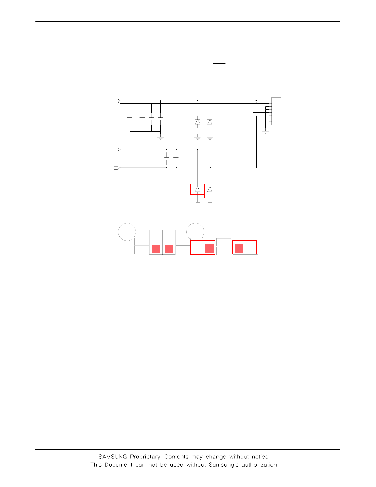
< Speaker / Receiver CON >
AMP_SPK_P
AMP_SPK_N
RCV_P
RCV_N
C548 C549
N
_
K
P
S
_
P
T
C550
C548
C550
C551
C541
Z
D
5
0
3
Z
D
5
0
2
ZD500
ZD502
C542
C551
C549
TP_SPK_P
TP_SPK_N
ZD503
ZD501
P
_
K
P
S
_
P
T
C542
C541
ZD500ZD501
1
2
3
4
5
6
7
8
SLC500
1
2
3
4
5
6
NC
NC
10-12
 Loading...